

用于在低电流密度下提高量子效率的 InGaN Micro-LED 结构设计
摘要
在这里,我们报告了氮化物微型发光二极管 (micro-LED) 在低电流密度下的工作行为和物理机制的综合数值研究。偏振效应分析表明,micro-LED在低电流密度下会受到更严重的量子限制斯塔克效应,这对提高效率和实现稳定的全色发射提出了挑战。分析载流子传输和匹配,以确定最佳工作条件并优化 micro-LED 在低电流密度下的结构设计。结果表明,有源区中较少的量子阱数会增强载流子匹配和辐射复合率,从而提高量子效率和输出功率。讨论了用于微型 LED 的电子阻挡层 (EBL) 的有效性。通过去除 EBL,发现电子限制和空穴注入同时得到改善,因此 micro-LED 在低电流密度下的发射显着增强。研究了Auger和Shockley-Read-Hall的复合过程,突出了micro-LED在低电流密度下对缺陷的敏感性。
概要 :数值研究了在低电流密度下工作的 InGaN micro-LED 的偏振诱导 QCSE、载流子传输和匹配以及复合过程。基于对这些器件行为和机制的理解,提出了专门设计的外延结构,包括两个 QW、高掺杂或无 EBL 以及具有高空穴浓度的 p-GaN,用于高效的 micro-LED 发光显示器。 micro-LED也突出了对缺陷密度的敏感性。
<图片>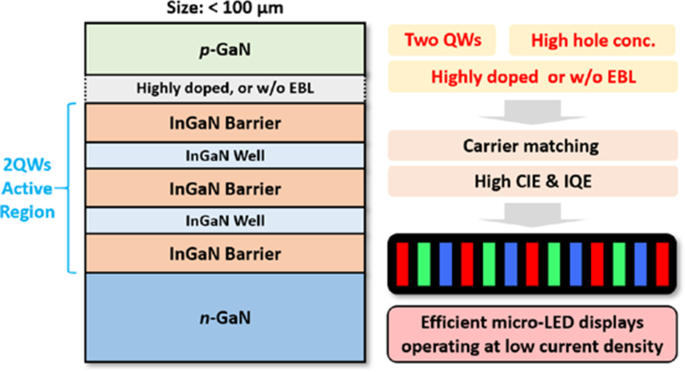
介绍
基于 III 族氮化物的可见光发光二极管 (LED) 具有广泛的应用,包括信号、光通信、信息存储、背光、显示器和普通照明(或固态照明)[1, 2]。自2000年Jiang及其同事首次演示直径为12μm的InGaN微盘LED [3, 4]以来,micro-LED在高分辨率显示领域得到了越来越广泛的学术和工业兴趣、可见光通信、生物医学和传感 [5,6,7,8]。与液晶显示器(LCD)和有机发光二极管(OLED)相比,micro-LED具有体积小、分辨率高、发光效率高、亮度高、色彩饱和度高、使用寿命长、响应速度快、和稳健性,使其成为下一代显示技术的最有希望的候选者 [9, 10]。 Micro-LED显示的应用场景包括高端电视(TV)、笔记本电脑、手持和移动终端设备、虚拟现实(VR)、增强现实(AR)、透明显示等。据Yole估计,到2025年Micro-LED显示屏市场将达到3.3亿片[11]。
III 族氮化物 LED 的传统应用,尤其是固态照明,要求光输出功率尽可能高 [12]。近三十年来,在大功率应用的推动下,氮化物LED的现代研究,包括外延结构的设计和优化,器件工作行为和物理机制的研究,以及制造技术的改进,主要集中在大芯片、高工作电流密度和高输入/输出功率[12, 13]。首先,氮化物LED的有源区已经从早期最简单的异质结构和单量子阱(QW)发展到今天的5周期QW的多量子阱(MQW),QW数甚至可以达到8或10个。商业化的大功率设备 [14,15,16,17]。提出 EBL 是为了在高注入电流密度下阻止电子泄漏,即使它也可以在一定程度上阻止空穴注入 [18, 19]。对于传统的大功率 LED,最重要的问题是随着电流密度的增加,外部量子效率 (EQE) 会降低,这被称为效率下降。这种行为的内在机制与高注入载流子密度下的间接俄歇复合有关 [20]。在制造方面,开发了薄膜倒装芯片和垂直注入几何形状以扩大氮化物 LED 的功率水平 [21, 22]。
传统的大尺寸高功率氮化物 LED 已经取得了长足的进步,其中一些经验教训可以用于 micro-LED 的研究。然而,微型 LED 与高功率的同类产品仍有很大不同。 Micro-LED 的不同操作行为、机制和条件会导致不同的挑战和研究路径 [23, 24]。对于传统 LED,峰值 EQE 位于高电流密度处,工作电流密度高且超出峰值效率 (> 30 A cm −2 )。但是对于micro-LED发光显示器,工作电流密度要低得多,通常在0.02到2 A cm −2 [24]。在这种低电流密度下,传统氮化物 LED 的 EQE 非常低,不足以满足实际的 micro-LED 显示应用。通过利用 V-pit 屏蔽位错和增强空穴注入的优势,Zhang 和他的合作伙伴创造了高效的基于 InGaN 的 LED,在 0.8 A/cm 2 时的峰值效率高达 24.0% .然而,Zhang 等人报道的 LED 芯片。仍然限于传统尺寸(1 mm × 1 mm),这远大于 micro-LED [25]。此外,许多工作报告称,微型 LED 的内部量子效率 (IQE) 和 EQE 随着芯片尺寸的减小而降低 [26,27,28]。这种与尺寸相关的退化主要归因于等离子体辅助干蚀刻引起的表面复合和侧壁损伤。这些侧壁效应有助于肖克利-读取-霍尔 (SRH) 非辐射复合,然后降低量子效率,并且由于比表面积/侧壁面积更大,因此在更小的芯片尺寸下变得更加严重。器件的活性区域 [29,30,31]。为了解决这个问题,提出了使用介电材料的侧壁钝化和使用缓冲氢氟酸或光电化学方法的湿法蚀刻,以将这些影响最小化到 micro-LED 的一定水平 [31,32,33]。然而,即使通过侧壁钝化改善,micro-LED(尺寸小于60μm)的峰值EQE仍然低于25%,并且在低于2 A cm的电流密度下急剧下降到几个百分点 −2 [34, 35]。特别是对于基于 InGaN 的红色 micro-LED,由于微型显示器的强偏振和较差的晶体质量 [0.2%),目前报道的 EQE 非常有限,低于 1%。 Appl Phys Express 14:011004" href="/articles/10.1186/s11671-021-03557-4#ref-CR36" id="ref-link-section-d295113462e757">36]。而且,随着芯片尺寸的缩小,峰值EQE的位置也向更高的电流密度移动,这将进一步阻碍低电流密度下的高效率[26]。
因此,在低电流密度下提高量子效率成为 micro-LED 发光显示应用的巨大挑战和关键科学问题。为此,应提高峰值效率,并将效率的起始位置转移到适当的较低电流密度。以前的工作主要集中在侧壁钝化等制造技术的改进上。为了提高效率,研究 micro-LED 在低电流密度下的工作行为和物理机制也很重要,这仍然是相对未探索和缺乏理解的。此外,要打造能够在低电流密度下最大提升效率的器件,micro-LED 的外延结构也需要重新设计和优化,这与它们传统的大尺寸高输入/输出对应物。目前,还缺乏专门为低电流密度工作的micro-LED发光显示器设计的外延结构。
在这项工作中,突出了 micro-LED 在低电流密度下运行的显示应用的独特挑战,并提出了解决这些问题的潜在解决方案。我们使用软件 Advanced Physical Model of Semiconductor Devices [37],数值研究了 InGaN micro-LED 在 200 到 0.1 A/cm 2 不同电流密度下的工作行为和物理机制 .对micro-LED的QCSE进行了能带图、波函数和极化场的模拟分析,证实了在低电流密度下的QCSE更严重。 QW数的影响,p 型掺杂浓度和 AlGaN EBL 对 micro-LED 的载流子传输、载流子匹配、辐射复合和量子效率进行了系统研究。还讨论了有关 SRH 和俄歇重组的影响和机制。在仿真分析的基础上,提出了一种专为micro-LED在低电流密度下工作而设计的优化外延结构。
设备结构和仿真方法
在本研究中,使用具有 60 × 60 μm 矩形芯片尺寸和 465 nm 附近峰值发射波长的蓝色 InGaN micro-LED 的常见结构进行模拟。图 1 显示蓝色 micro-LED 由 200 nm n 组成 -GaN 层,MQWs 有源区,20 nm p -Al0.15Ga0.85 N EBL 和 150 nm p -GaN层。 MQW 有源区由 8、5、3、2 或 1 个周期组成,其中 2.5 纳米厚的 In0.25Ga0.75 N QW 嵌入在 10 纳米厚的 In0.05Ga0.95 N 量子势垒 (QB) 中。 MQW 的 In 成分经过调整和优化,以实现所需的蓝色发射波长。 n的掺杂浓度 -GaN,p -AlGaN EBL 和 p -GaN为2 × 10 18 厘米 −3 , 3 × 10 18 厘米 −3 , 和 1 × 10 19 厘米 −3 , 分别。
<图片>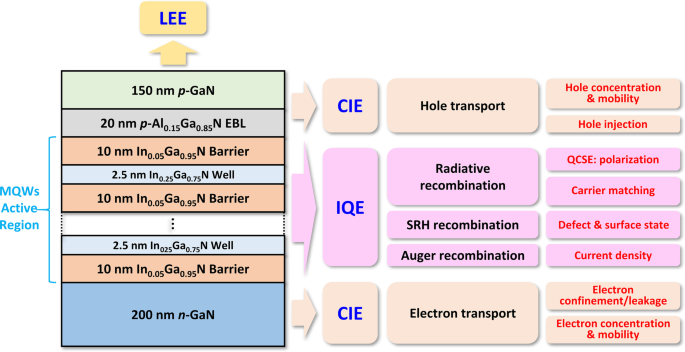
用于LED模拟和效率分析的InGaN/GaN基蓝光发光二极管示意图
使用软件先进的半导体器件物理模型 [37] 对微型 LED 的光学和电学特性进行了数值研究。在模拟中,假设 50% 的界面电荷密度由自发极化和压电极化引起 [38]。除了特别提到的,SRH寿命和俄歇复合系数设置为100 ns和1 × 10 –31 厘米 6 s −1 , 分别 [39, 40]。假设带偏移比为 0.7/0.3 [41],光提取效率固定为 70%,工作温度为 300 K。模拟中使用的其他材料参数可以在参考文献 [42] 中找到。
结果和讨论
LED 的插墙效率 (WPE) 可以表示为:
$${\text{WPE}} =\frac{{P_{{{\text{out}}}} }}{{I_{{{\text{op}}}} \times V}} =\eta_ {{{\text{EQE}}}} \frac{\hbar \omega }{{e \times V}} =\eta_{{{\text{EQE}}}} \times \eta_{{{\text {选择}}}} ,$$ (1)其中 P out 表示光输出功率,I op 是工作电流,V 是驱动电压,ℏω 是光子能量,η 选择是电效率。 EQE η EQE 是电流注入效率 (CIE) η 的乘积 CIE、IQE η IQE 和光提取效率 (LEE) η 李 ,由以下等式描述:
$$\eta_{{{\text{EQE}}}} =\eta_{{{\text{CIE}}}} \times \eta_{{{\text{IQE}}}} \times \eta_{{ {\text{LEE}}}} .$$ (2)此外,根据 ABC 模型 [43],η IQE 可以表示为:
$$\eta_{{{\text{IQE}}}} =\frac{{R_{{{\text{rad}}}} }}{{R_{{{\text{rad}}}} + R_ {{{\text{SRH}}}} + R_{{{\text{Auger}}}} }},$$ (3)其中 R rad 是辐射复合率,R SRH 是 SRH 非辐射复合率,R 俄歇是俄歇重组率。图1显示了不同类型的效率及其相关的物理机制和因素。
R rad 和 CIE 必须最大化,电效率和 LEE 必须提高,SRH 和俄歇复合必须减少,以提高 micro-LED 在低电流密度下的整体效率。需要系统级方法来解决所有这些挑战。除了光提取之外,这些挑战将在以下部分中讨论,并且还将提出创建有效的 micro-LED 外延结构的潜在解决方案。
低电流密度下的 QCSE:内部极化场
偏振诱导的 QCSE 是限制氮化物 LED IQE 的主要因素之一 [44]。 QCSE 已经针对传统的大尺寸大功率 LED 进行了广泛的研究,但在 micro-LED 特定应用的背景下仍然缺乏足够的讨论。因此,首先研究这个重要的影响。这里讨论的 micro-LED 的有源区由 5 个周期的 QW 构成,这是传统氮化物 LED 最常用的 QW 数。
图 2a 显示了在 200 和 0.1 A/cm 2 时第五 QW 的能带图和相关的一级电子和空穴波函数 . QB 和 QW 经历大的波段弯曲,导致电子和空穴波函数的空间分离。此外,在低电流密度下能带弯曲更强,表明 QCSE 更强。这种现象归因于在低注入电流密度下具有较少非平衡载流子的弱屏蔽效应(参见附加文件 1:图 S1a-d 和相关讨论)[41]。图 2b 显示更严格的 QCSE 增强了低电流密度下载波函数的空间分离,从而导致较低的辐射复合率。辐射复合率和 EL 光谱没有和有极化效应,即没有和有 QCSE,进一步计算以显示电子 - 空穴分离如何在低电流密度下定量减少发射。图 2c、d 显示辐射复合率和 EL 强度的积分强度分别通过 QCSE 降低了约 84.0% 和 72.3%。这些结果表明,由于在低电流密度下增强了 QCSE,micro-LED 比传统的高功率耦合更难提高效率。
<图片>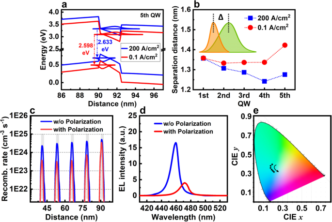
一 在 200 和 0.1 A/cm 2 时第五 QW 的能带图和相关的一级电子和空穴波函数 , 分别。 b 200和0.1 A/cm时电子和空穴波函数峰值位置的分离距离 2 , 分别。 c 辐射复合率和 d EL 光谱在 0.1 A/cm 2 分别没有和有极化。 e 由蓝色、绿色和红色 LED 产生的色点,电流密度为 0.1 至 20 A/cm 2 绘制在 1931-CIE (x, y) 色度图上
此外,在不同注入电流密度下准确稳定地控制发射波长对于 micro-LED 显示至关重要,因为它决定了各种重要参数,如亮度、色彩精度和饱和度。然而,在低电流密度下更严格的 QCSE 使这成为一个巨大的挑战,特别是对于需要更高铟成分的绿色和红色微型 LED。作为具有更高铟成分和更强 QCSE 的 InGaN QW 中增加的能带弯曲的直接结果,由于屏蔽效应,波长偏移与电流密度的关系变得更加明显。进一步计算了具有各种电流密度的基于 InGaN 的红色、绿色和蓝色微型 LED 的 EL 光谱,以显示光谱偏移如何影响显示器中的色点。附加文件 1:图 S2 显示从 0.1 到 20 A/cm 2 ,红色、绿色和蓝色微型 LED 的峰值波长蓝移分别约为 15.8、6.6 和 1.7 nm。还计算了通过组合红色、绿色和蓝色微型 LED 创建的色点,如附加文件 1:表 S1 中所述。图 2e 说明了相应的 1931-CIE (x, y) 色度图。显然,当电流密度增加时,RGB micro-LED 的发射颜色从绿色显着变化为蓝绿色。 1931-CIE x 值从 0.1676 交叉到 0.2084,1931-CIE y 值从 0.3891 交叉到 0.3106。这种色点与电流密度的显着变化极大地降低了micro-LED显示器的性能。
许多报告提出了几种抑制 QCSE 的方法,例如使用 InGaN/AlGaN 超薄超晶格势垒 [45]、具有 GaN 层间势垒的 InGaN/GaN/AlGaN/GaN MQWs [46]、皱纹 MQWs [47] 和插入MQW 之前的应变释放层 [48]。但是 QCSE 是由 c 的内在属性引起的 -平面氮化物材料。 MQW 的几次调整不足以完全抑制这种影响。最近,非极性氮化物 LED 已经获得了不错的效率。如果能够降低非极性GaN衬底的成本,非极性LED可以成为降低QCSE和实现稳定全彩发射的理想解决方案[49]。
载波传输与匹配
电子 (J n ) 和孔 (J p ) 电流密度可以表示为:
$$J_{n} =\sigma_{n} \left| {\varvec{E}} \right| =nq\mu_{n} \left| {\varvec{E}} \right|,$$ (4) $$J_{p} =\sigma_{p} \left| {\varvec{E}} \right| =pq\mu_{p} \left| {\varvec{E}} \right|,$$ (5)其中 σ n 和 σ p 表示电导率,n 和 p 是浓度,μ n 和 μ p 分别是电子和空穴的迁移率,E 表示电场。在氮化物中,空穴浓度比电子[50]低一个数量级,空穴迁移率比电子低两个数量级[51]。这种浓度和迁移率的不对称导致载流子通量 (J n> J p ) 并通过以下两种方式降低 LED 的性能。
电流注入效率 :当前喷射效率η CIE代表复合电流的比值J 重新组合到总电流 J 总计,如下等式[52]:
$$\eta_{{{\text{CIE}}}} =\frac{{J_{{{\text{recomb}}}} }}{{J_{{{\text{total}}}}}} =\frac{{J_{{n{\text{ - recomb}}}} + J_{{p{\text{ - recomb}}}} }}{{J_{n} + J_{p} }} =\frac{{2 \times J_{p} }}{{J_{n} + J_{p} }}.$$ (6)J 重组取决于载流子电流中较小的一个,即空穴电流。等式 (6) 证实了载波失配 (J n> J p ) 限制了 CIE 的最大化。
辐射复合率 :辐射复合率R rad 由费米的黄金法则描述为以下等式:
$$R_{{{\text{rad}}}} =C \times \smallint {\text{d}}E_{cv} hv_{cv} \left| {\overline{{M_{T} }} \left( {E_{cv} } \right)} \right|^{2} \rho_{r} \left( {E_{cv} } \right)f_{ v} \left( {1 - f_{c} } \right),$$ (7)其中 C 是一个常数,E 简历 是跃迁能,h 是普朗克常数,ν 简历 是产生光的频率,ρ r 是减少的态密度,f c 和 f v 是费米-狄拉克分布,|M T | 2 是动量矩阵元素[53]。 QW 中较少的空穴和额外的电子积累会导致晶格膨胀和拉伸应变的积累。在这种应力变化下,价带最大值附近的量子能级的电荷密度降低。这进一步降低了光学跃迁概率并降低了 R rad 根据方程。 (7).以这种方式,单个 QW 中的本地载波不匹配也限制了 IQE。关于这个话题更具体的讨论可以在之前的报告中找到[54,55,56]。
在以下部分中,QW 数的影响,p 型掺杂浓度,以及载流子传输上的 EBL 结构将被分析,以确定最佳载流子匹配条件。最后,将提出一种优化的外延结构,用于在低电流密度下工作的高效 micro-LED 显示器。
5QW 中的载波不匹配
首先,模拟了具有 5QW 的蓝色微型 LED 的载流子传输特性。 200 A/cm 2 载流子浓度分布 和 0.1 A/cm 2 分别在附加文件 1:图 S3a 和 b 中说明。在高和低电流密度下都可以观察到 5 个 QW 的不均匀分布。附加文件 1:图 S3c 和 d 显示 MQW 中的电子迁移率 (684 cm 2 V −1 s −1 ) 比空穴迁移率 (10 cm 2 V −1 s −1 )。因此,电子可能只是注入,然后通过MQW而不参与复合,导致电子泄漏问题和低CIE [51]。
图 3a 显示了 200 A/cm 2 时电子和空穴电流密度的分布 .总空穴电流密度 (217.4 A/cm 2 ) 仅为电子的 65.2% (333.3 A/cm 2 ),表明载波严重不匹配和低 CIE。漏电子电流高达116.0 A/cm 2 ,这会降低辐射效率和空穴注入。如图3b所示,漏电子电流仅为0.01 A/cm 2 , 和计算出的 η CIE 在 0.1 A/cm 2 时高达 95% .这些结果表明在低电流密度下更容易实现高 CIE。但是,除了 J 的第 5 个 QW p 可以等于 J n ,在高电流密度和低电流密度下,其他四个 QW(QW 1、2、3 和 4)的载流子失配和额外的电子积累都非常严重。 200 A/cm 2 ,这四个 QW 的电子电流密度分别是空穴电流密度的 120、43、16 和 5 倍(图 3a)。在 0.1 A/cm 2 ,它们比空穴电流高 23、9、4 和 2 倍(图 3b)。基于方程。 (7),这种严重的载波失配明显降低了这四个 QW 的辐射复合率。因此,这四个 QW 的辐射复合率在 200 A/cm 2 时分别约为 3.4%、4.0%、10.1% 和 34.2% , 11.3%, 10.1%, 10.7% 和 21.2% at 0.1 A/cm 2 与第 5 个 QW 相比。这些载流子失配和低辐射最终降低了micro-LED的单片效率。
<图片>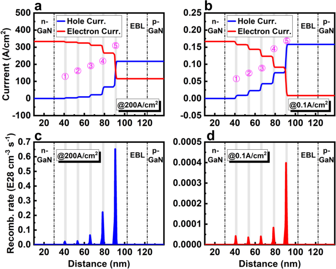
5QW的LED载流子电流分布a 200 A/cm 2 和 b 在 0.1 A/cm 2 .具有 5QWs c 的 LED 的辐射复合率 200 A/cm 2 和 d 在 0.1 A/cm 2
影响载体运输和匹配的因素
QW 编号 :对于在高电流密度下运行的传统大尺寸 LED,必须使用 5、甚至 8 或 10 个周期的 MQW 来实现高光输出功率。然而,对于micro-LED发光显示器来说,输出功率要小得多,工作电流密度要低得多。如上一节所述,即使在低电流密度下,5QW 中的载流子失配仍然非常严重,并且只有一个 QW 可以达到最佳匹配条件。从这个角度来看,对于在低电流密度下工作的micro-LED,由于载流子匹配的改善,QW数较少的有源区应该是提高效率的更好设计。
研究 QW 数对微型 LED 的影响以验证我们的假设。图 4a-f 显示了载流子电流密度和辐射复合率在 0.1 A/cm 2 分别具有 3QW、2QW 和 1QW 的 LED。当前曲线只有一个交点(最佳载波匹配点,J n =J p ) 由于电流的单调下降趋势,但 QW 较少,如 3QW 和 2QW 的情况,可以在两个不同的 QW 中实现两个交点(图 4a、b)。换句话说,MQW 中的载波不匹配可以通过较少的 QW 部分克服。特别是对于2QWs,通过适当的调整,可以在所有两个QWs中实现载流子通量的完美匹配。 2QW 中的辐射复合率也高于 3QW 和 5QW,因为辐射复合的载流子消耗更集中在 QW 较少的有源区(图 3d、4d、e)。毫无疑问,最好的载流子匹配是在只有一个 QW 的 LED 中,而 1QW 的辐射复合率也最高,如图 4c、f 所示。
<图片>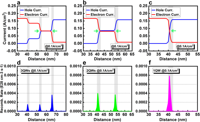
带有a的LED载流子电流分布 3QW,b 2QW 和 c 1QW 在 0.1 A/cm 2 . LED 与 d 的辐射复合率 3QW,e 2QW 和 f 1QW 在 0.1 A/cm 2
图 5a、b 显示了 IQE 作为 0 到 200 A/cm 2 之间电流密度的函数 和 0 到 10 A/cm 2 , 分别。对于高于 50 A/cm 2 的电流密度 , 当 QW 数减少时 IQE 减少。相比之下,电流密度低于约 30 A/cm 2 的 IQE QW 数减少时增加。在 0.1 A/cm 2 , 8、5、3、2 和 1 个 QW 的 IQE 值分别为 55%、62%、69%、77% 和 78%。此外,如图 5b 所示,峰值 IQE 的位置也从 6.0 A/cm 2 在 8 QWs 到最低电流密度大约 1.2 A/cm 2 在 2QW。低电流密度下的 IQE 曲线 (<1 A/cm 2 ) 也随着 QW 数的降低而变得更陡峭和尖锐,这表明实现最高效率更容易、更快捷。这对于提高低电流密度下的效率非常有利。 IQE 这种趋势背后的物理机制可以通过载流子通量的更好匹配以及 QW 数较少的有源区域中更集中、更强的辐射发射来解释。如图5c所示,与8个QW相比,0.1 A/cm 2 下5、3、2和1个QW的积分EL强度 分别增长约 6.1%、14.8%、28.4% 和 32.1%。这一结果证实,QW数量较少,不仅效率提高,输出功率也提高。
<图片>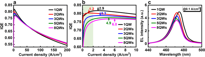
一 IQE 曲线和 b 具有 8、5、3、2 和 1 个 QW 的 LED 在低电流密度下的 IQE 曲线。 c 具有 8、5、3、2 和 1 个 QW 的 LED 在 0.1 A/cm 2 的 EL 光谱
仿真结果表明,1QW 具有最高的 EL 强度,可能是在低电流密度下运行的 micro-LED 的最佳结构。然而,在实验上,很难外延生长一个具有平坦表面和尖锐界面的 QW。此外,对于 1QW 结构,峰值 IQE 的位置略有增加至 2.9 A/cm 2 ,IQE曲线的形状也略有变化。这可以用单QW的特殊情况来解释。与其他 QW 相比,与 EBL 相邻的 QW 具有特殊的极化环境,被认为是“问题 QW”。此主题将在 AlGaN EBL 部分详细讨论 .考虑到这些原因,2QWs 应该是最好的有源区设计,它具有类似的良好匹配载流子通量,接近 IQE 值,以及 EL 强度到 1QW。因此,在以下部分中,所有模拟均基于具有 2QW 的 micro-LED。
P-GaN 掺杂浓度 :不同p的2QWs LED的性能 p 中的 -type 掺杂浓度 -GaN被进一步研究。如图6a所示,当p的掺杂浓度 -GaN 从 1 × 10 18 增加 厘米 −3 到 5 × 10 19 厘米 −3 , 0.1 A/cm 2 时的辐射复合率 两个 QW 进一步增加约 3.1% 和 3.0%。图6b显示总空穴电流密度从0.157增加到0.162 A/cm 2 , 同时漏电子电流密度从 0.009 降低到 0.005 A/cm 2 随着掺杂浓度的增加。值得注意的是,QW 中 n 附近的复合电流 -side 高于 p 附近的 QW -侧(图6b)。因此,n附近的辐射复合率 -side QW 也略高于 p 附近的 -侧QW。如图 6c 所示,可以发现 EBL 中载流子的能垒,定义为电子/空穴准费米能级与最高导带或最低价带之间的能量距离,在不同的条件下几乎没有变化。 p的掺杂浓度 -GaN,即空穴注入并没有通过增加掺杂浓度而得到改善。图 6d 显示了 p 中的平均空穴浓度 -GaN 和 QW。 p 中的空穴浓度 -GaN几乎与掺杂浓度呈指数关系。 Inside the QWs, the hole concentration is increased approximately twice from 1.59 × 10 19 厘米 −3 to 3.08 × 10 19 厘米 −3 with a higher doping concentration. These results indicate that the increased hole concentration is the main contribution for the improvement of radiative recombination. Therefore, even at low current density, the p -type doping problem of nitride remains notable, and enhancing the doping efficiency and hole concentration is still beneficial for the efficiency of micro-LED.

一 Radiative recombination rates of 2QWs LED with various doping concentrations in p-GaN. b Carrier current distribution with different doping concentrations in p -GaN. c Enlarged energy band diagrams of EBL with different doping concentrations in p -GaN. d Average hole concentration in p -GaN and QWs with various doping concentrations of p -GaN
AlGaN EBL :In the last decades, a 10–20 nm p -type AlGaN EBL has become a standard structure for traditional nitride-based LEDs. This EBL is considered to block the electron leakage and suppress the efficiency droop under high injected current density. In spite of this, it is worth noting that the EBL is still a very complicated, subtle structure for the LED. It involves many important factors, including Al composition, p -type doping efficiency of AlGaN, band offset ratios, and polarization effect. Each of them can influence the band structure and carrier transport substantially, then determines the effectiveness of EBL. For the construction of EBL, thickness, composition, and doping concentration must be considered and optimized carefully to balance the enhancement of electron confinement and the blocking of hole injection, otherwise, the opposite may happen, and the performance of LED might deteriorate. For micro-LED, the effectiveness of EBL for operating at low current density must be reconsidered, which may be different with the case of traditional high input/output LED.
a. Doping concentration of EBL :First, the effect of EBL doping concentration on carrier transport at low current density is investigated. The thickness and Al composition of EBL are fixed as 20 nm and 0.15, respectively. Considering the low solubility of Mg dopant in AlGaN, the crystal degradation, and compensation effect by over-doping [50], the doping concentration of EBL is first set as be 3 × 10 18 厘米 −3 . Figure 7a shows the corresponding energy band structure. Clearly, despite the existence of EBL, the electron leakage out of the QW still can be caused by the insufficient electron confinement due to the downward bending of the last QW and EBL. A new energy valley under the electron quasi-Fermi level appears at the interface of last QB and EBL. Thus, electrons would escape from QW and accumulate in this area. This distortion of band structure makes the EBL relatively ineffective, and it can be contributed to the polarization effect. As shown in Fig. 7c, the strong polarization induces a large amount of charges at the interfaces. Due to the unbalanced polarization charges are positive at the interface of the last QB/EBL, a large electrostatic field pointing from the p -side to the n -side builds up in the last QB, which is opposite to the fields in other QBs and EBL. These electrostatic fields pull down the energy band of the last QB and EBL. Moreover, the electric fields in the last QW and last QB both can attract electrons and drive them out of the active region into the p -layer. This can be observed in the carrier concentration diagram, as shown in Fig. 7d. The dotted black line indicates that a part of the electrons escape from the active region and accumulate at the interface of last QB/EBL. In the EBL and p -GaN, the leakage electron remains relatively high.

Energy band diagrams of 2QWs LED with a 3 × 10 18 厘米 −3 和 b 6 × 10 19 厘米 −3 doping concentration in AlGaN EBL. c Space charge density and d carrier concentration distribution of 2QWs LED with 3 × 10 18 and 6 × 10 19 厘米 −3 doping concentration of EBL. The inset of c shows the direction of polarization fields
On the other hand, the EBL also introduces a potential barrier as high as 480 meV for hole injection. Moreover, as shown in Fig. 7a, c, an energy valley close to the hole quasi-Fermi level appears at the interface region between the EBL/p -GaN due to the polarization effect. As indicated by the solid black line of Fig. 7d, most of the holes are blocked by the EBL and thus, accumulate at the energy valley of the EBL/p -GaN interface. Owing to this inefficient carrier transport, the last QW is considered as a “problem QW,” and the EBL only has a low capability for electron confinement, and should be responsible for the poor hole injection. Compared with the traditional high input/output LED, this polarization induced ineffectiveness of the EBL function could be particularly severe for the micro-LED due to the enhanced polarization effect by less carrier screening at low current density.
Band engineering by increasing the doping concentration of EBL is a possible method to improve the electron confinement and hole injection. The activation energy of Mg dopant in AlGaN EBL is higher than GaN, therefore, even under a similar doping concentration, the active hole concentration in EBL remains much lower than p -GaN. The lower hole concentration could further separate the hole quasi-Fermi level and valence band, then increase barrier height. Based on this analysis, the doping concentration of EBL needs to be much higher than p -GaN. Considering the doping limitation in actual experiment, 6 × 10 19 厘米 −3 is selected as a new doping concentration in the EBL. As shown in Fig. 7b, by increasing the doping concentration, the valence band of EBL is lifted due to the alignment of hole quasi-Fermi level, resulting in a reduced hole energy barrier of 281 meV. Moreover, the high p -type doping also helps lower the electron quasi-Fermi level with respect to the conduction band in EBL, hence increasing the effect barrier for electron leakage to 1175 meV. These changes improve electron confinement and hole injection. Figure 7d shows that compared with the doping concentration of 3 × 10 18 厘米 −3 , the hole concentration in the active region is greatly increased, and the leakage electron in the EBL and p -GaN is reduced to almost zero. However, the energy valley at the interface between the EBL/p -GaN still exists. Moreover, the upward of valence band also introduces a new energy valley for the hole accumulation at the interface between the last QB/EBL, which can be confirmed by the hole concentration distribution in Fig. 7d. These energy valleys can impede the hole injection into QWs, hence compensating the advantage of high doping concentration.
b. Al composition of EBL :Compared with the increase of doping concentration, reducing the composition of AlGaN EBL may be an easier, more efficient method to improve the carrier transport at low current density. The effectiveness of EBL is sensitively dependent on Al composition, band offset, and polarization effect. Increasing the Al composition of EBL can increase the band offset between the last QB/EBL, which increases the electron barrier height. However, as shown in Fig. 8a, the polarization-induced charges at the interfaces also increase accordingly, which pull down the electron barrier height. Two mechanisms have the opposite effect for confining electrons.

一 Space charge density distribution of 2QWs LED with different EBL. The inset shows the direction of polarization field. Energy band diagrams of 2QWs LED b with Al0.1Ga0.9 N EBL and c without EBL. d Carrier concentration distribution, e carrier current density, f IQE and g EL spectra of 2QWs LED with different EBL. The inset of g shows the working voltages at 0.1 and 1 A/cm 2 with different EBLs
Based on this analysis, the carrier transport of 2QWs micro-LEDs with different EBL structures at 200 and 0.1 A/cm 2 are investigated. The result of effective energy barrier heights of different EBL are summarized in Table 1. First of all, both the electron and hole energy barriers at low current density are much higher than the cases of at high current density due to the lower nonequilibrium carrier population. A higher energy barrier can improve the electron confinement, but also severely impedes the hole injection at low current density. This indicates that the influence of EBL on the carrier transport of micro-LED operating at low current density is much higher than that of the traditional high input/output LED. Table 1 also shows that with a relatively low Al composition in EBL, the electron barrier decreases with Al composition increased, which indicates that the downward of conduction band induced by polarization effect is larger than the increased band offset introduced by the higher Al composition. By further increasing the composition, the electron barrier increases along with composition, meaning that the band offset becomes dominant over the polarization effect. Compared with high current density, this turning point of composition is higher at low current density due to the enhanced polarization effect by less carrier screening. On the other hand, because of the original band offset between the last QB/p -GaN and the band bending, there are energy barriers for electron and holes exist at the interface even without the EBL. At 200 A/cm 2 , when the composition is lower than 0.20, the electron energy barrier is lower than the case of without EBL, but the hole barrier is higher approximately 64 meV. At 0.1 A/cm 2 , even with composition higher than 0.20, the electron barrier of AlGaN EBL (523 meV) is still 151 meV lower than the case of without EBL (674 meV), but the hole barrier is increased approximately 76 meV from 409 to 485 meV. These results indicate that both the electron confinement and hole injection could be deteriorated by the EBL with an incorrect composition, especially for micro-LED operating at low current density.
For a deep analysis, band structures of micro-LEDs with Al0.10Ga0.90 N EBL and without EBL as representatives are illustrated in Fig. 8b, c. The EBL introduces two energy valleys at the interface of last QB/EBL and EBL/p -GaN for electron and hole accumulation, respectively, which can be confirmed by the carrier concentration diagram in Fig. 8d. Therefore, the electron confinement and hole injection are poor for this structure. When the EBL is removed, as shown in Fig. 8c, the energy barrier for electron is increased, and the energy valley for electron extracting and accumulation disappeares. These changes prevent electrons leakage more effectively, as confirmed in Fig. 8d. Meanwhile, the barrier height for hole injection is reduced, and the energy valley at the EBL/p-GaN interface is also removed. So, the hole can transport directly into the QW without facing large obstacle, as shown in Fig. 8c, d.
The above careful investigation suggests that without EBL may be a better structure for the micro-LED operating at low current density. Simulation results support our suggestion. Figure 8e illustrates the carrier current density at 0.1 A/cm 2 with different EBL structures. When the Al composition of the EBL is reduced from 0.15 to 0.04, the total electron and hole current densities increase from 0.167 and 0.159 A/cm 2 to 0.225 and 0.225 A/cm 2 , 分别。 Moreover, when the EBL is completely removed, both the total electron and total hole current densities greatly increase to 0.528 A/cm 2 , which is approximately 3 times higher compared with the Al0.15Ga0.85 N EBL. This enhancement is contributed to the improved electron confinement and hole injection.
Figure 8f shows the IQE curves at low current density. When the Al composition of EBL is reduced from 0.15 to 0.04, the IQE values increase evidently due to the improved carrier transport. However, by removing the EBL, the IQE value experiences a slight decrease compared with Al0.04Ga0.96 N EBL. This can be explained by the carrier matching in two QWs. As indicated by the green arrows in Fig. 8e, a, perfect carrier matching occurred in both the two QWs with Al0.04Ga0.96 N EBL. With the increase of current density by removing EBL, the matching of electron and hole flux has been slightly broken in the first QW, where the electron current density is slightly higher than the hole. Therefore, the IQE is slightly reduced because of this carrier mis-matching in one QW.
The superiority of micro-LED without EBL is still remarkable due to the improved carrier transport. As shown in Fig. 8g, at 0.1 A/cm 2 , the integral EL intensities of micro-LED without EBL are 3.53, 3.23, and 2.38 times higher compared with the LED with Al0.15Ga0.85 N, Al0.10Ga0.90 N and Al0.04Ga0.96 N EBL, respectively. Moreover, as shown in the inset of Fig. 8g, the working voltages under 1 A/cm 2 and 0.1 A/cm 2 are reduced about 0.53 V and 0.57 V by removing the EBL, respectively. This improves the electrical efficiency, then finally increases the WPE of micro-LED. To further confirm that the EBL-free structure is a better design for micro-LED operating at low current density, another simulation is performed using the reported blue micro-LED structure with maximal known efficiency. The results and discussions can be found in the Supporting Materials (Additional file 1:Fig. S4a-d).
Optimized Structure for Micro-LED Operating at Low Current Density
Based on above simulation and analysis, the optimized epitaxial structure specifically designed for the efficient micro-LED emissive display operating at low current density is proposed, as shown in Fig. 9. Three principles must be followed. First, in contrast to the traditional large-size high-power nitride LED, the QW number of micro-LED should be reduced to just two, which has a better condition for the carrier matching, a more concentrated radiative emission, and higher IQE and WPE. Second, the p -type doing still needs to be enhanced due to the relatively low hole concentration and mobility compared with the electron in nitride, which demands a more efficient p -type doping strategy. Third, to improve the carrier transport and matching, the doping concentration of AlGaN EBL should be greatly enhanced, or the AlGaN EBL can be completely removed. Without using the AlGaN EBL, the electron confinement, hole injection, carrier matching, IQE, and WPE of the micro-LED can be greatly improved at low current density.

Schematic illustration of the optimized epitaxial structure designed specifically for the micro-LED emissive displays operating at low current density
Auger Recombination and SRH Non-radiative Recombination
基于方程。 (3), except for radiative recombination, the SRH and Auger recombination also play critical roles in the IQE of LED. Hence, it is important to investigate the effects and mechanism regarding the SRH and Auger recombination for the micro-LED. In this part, the LED structure with 2QWs is still used, and all the simulation parameters are the same as mentioned in the Methods except for SRH lifetimes.
Negligible Auger and Prominent SRH Recombination
The SRH recombination rate can be expressed as follows [57]:
$$R_{{{\text{SRH}}}} =\frac{{np - n_{i}^{2} }}{{\tau_{p} \left( {n + n_{i} \exp \left( {\frac{{E_{T} }}{kT}} \right)} \right) + \tau_{n} \left( {p + n_{i} \exp \left( {\frac{{E_{T} }}{kT}} \right)} \right)}},$$ (8) $$\tau_{p} =\frac{1}{{c_{p} N_{t} }}, \tau_{n} =\frac{1}{{c_{n} N_{t} }},$$ (9) $$c_{p} =\sigma_{p} \nu_{p} , c_{n} =\sigma_{n} \nu_{n} ,$$ (10)其中 n 我 is the intrinsic carrier concentration, τ p 和 τ n are the hole and electron SRH lifetimes, respectively, E T is the energy difference between the trap level and the intrinsic Fermi level, c p 和 c n are the capture coefficients for electron and hole, N t is the trap density, σ p 和 σ n are capture cross sections for electron and hole, and ν p and ν n are the average thermal velocities of electron and hole, respectively. According to Eqs. (8)-(10), the SRH recombination of a trap is completely specified by its density, capture cross sections and energy level.
The Auger recombination rate is given by the following:
$$R_{{{\text{Auger}}}} =\left( {C_{n} n + C_{p} p} \right)\left( {np - n_{i}^{2} } \right),$$ (11)其中 C n 和 C p are the Auger recombination coefficients.
Given that the injected hole and electron concentrations are much higher than the intrinsic carrier concentration in the undoped QWs (according to simulation result, the highest carrier concentration in QW is only approximately 10 7 厘米 −3 in the absence of externally injected current), the SRH and Auger recombination rate can be further simplified as the following equations:
$$R_{{{\text{SRH}}}} =\frac{np}{{\tau_{p} n + \tau_{n} p}},$$ (12) $$R_{{{\text{Auger}}}} =\left( {C_{n} n + C_{p} p} \right)np.$$ (13)Equations (12) and (13) clearly show that R SRH is in direct proportion to the first power of the carrier concentration, but R Auger depends on the third power of the carrier concentration, that is, R SRH is sensitive to low current density, while the R Auger is more dominant at high current density.
This theoretical analysis agrees with our simulation results. Figure 10a, b shows the calculated radiative, SRH, and Auger recombination rates at 200 and 0.1 A/cm 2 , 分别。 At high current density, the Auger recombination rate (about 0.8–1.4 × 10 29 厘米 −3 s −1 ) is comparable wiht the radiative rate (about 4.2–6.0 × 10 29 厘米 −3 s −1 )。 In fact, the substantial problem of efficiency droop at high drive currents is now widely acknowledged as caused by the Auger recombination [20]. While, at low current density, relatively, the Auger recombination rate dramatically decreases to two orders of magnitude lower (about 6.3–7.2 × 10 22 厘米 −3 s −1 ) than the radiative recombination (about 3.7–4.0 × 10 24 厘米 −3 s −1 )。 Therefore, the Auger recombination should be negligible at low current density. Conversely, with the decrease of current density, the SRH recombination rate relatively increases from a small value at 200 A/cm 2 (two orders of magnitude lower than radiative recombination) to a level comparable with the radiative emission at 0.1 A/cm 2 . As a result, the micro-LED operating at low current density requires improvement in the SRH or defect recombination instead of the Auger recombination.

Radiative, SRH, and Auger recombination rates of 2QWs LED a at 200 A/cm 2 和 b at 0.1 A/cm 2 . c SRH/Radiative ratio with various SRH lifetimes at 200 and 0.1 A/cm 2 . d IQE values at 200 and 0.1 A/cm 2 , e IQE curves with large current density and f IQE curves with low current density at various SRH lifetimes
Requirement for Low Defect Density
根据方程。 (9), SRH lifetimes, τ p 和 τ n , are in inverse proportion to the density of defects N t . Therefore, the effect of defect density can be estimated by simply changing the SRH lifetime in the simulation. Figure 10c shows the calculated ratio of SRH/radiative recombination rate at various SRH lifetimes. With the decrease of SRH lifetimes from 150 to 50 ns, i.e., the increase of defect density, the SRH/radiative ratio slightly increases from 0.01 to 0.03 at 200 A/cm 2 , but greatly increases from 0.15 to 0.43 at 0.1 A/cm 2 . This means that a much larger percentage of carriers is consumed by the trapping defects at low current density. Therefore the efficiency is much more sensitive to the defect density at low current than high current density. The IQE results as shown in Fig. 10d, e confirm this trend. With the decrease of SRH lifetimes from 150 to 50 ns, IQE only decreases about 0.01 at 200 A/cm 2 , but dramatically decreases about 0.17 at 0.1 A/cm 2 . Moreover, as shown in Fig. 10f, with the decrease of SRH lifetime, the position of peak IQE also moves from 3.1 A/cm 2 to a higher current density of 9.0 A/cm 2 , and the IQE curves become less steep and sharp, which means that the threshold/onset current is increased. This is disadvantageous for improving the efficiency of micro-LED at low current density.
Compared with the traditional large-size high-power LED working at high current density, the micro-LED operating at low current density is much more sensitive to defect density, and minimizing the defect recombination is of paramount importance for achieving a high efficiency. Therefore, the micro-LED requires a much more higher crystal quality of materials than the traditional LED, and poses large challenges for the epitaxial growth of the material and the fabrication of the device for the community.
结论
In summary, the operating behaviors, mechanisms and conditions of InGaN micro-LED operating at low current density are numerically investigated, and an optimized epitaxial structure specifically designed for the micro-LED display is proposed. Analysis of the polarization effect shows that micro-LED suffers a severer QCSE at low current density. Hence, improving the efficiency and controlling the emission color point are more difficult. Carrier transport and matching are analyzed to determine the operating conditions of micro-LED. It is shown that less QW number can improves the carreir matching and leads to higher efficiency and output power at low current density. Effectiveness of the EBL for micro-LED is analyzed, and electron confinement and hole injection are found to be improved simultaneously at low current density by removing the EBL. Moreover, simulaiton has shown that the Auger recombination is negligible, but the SRH recombination greatly influences the efficiency of micro-LED at low current density, which has raised higher requirements for the crystal quality of materials and the fabrication process of devices. Our numerical study can provide valuable guidance for creating efficient micro-LED display and promote future research in this area.
数据和材料的可用性
The data and the analysis in the current work are available from the corresponding authors on reasonable request.
缩写
- Micro-LED:
-
Micro-light-emitting-diode
- QCSE:
-
Quantum-confined Stark effect
- EBL:
-
Electron blocking layer
- SRH:
-
Shockley–Read–Hall
- LCD:
-
Liquid–crystal display
- OLED:
-
Organic light-emitting diode
- TV:
-
Televisions
- VR:
-
Virtual reality
- AR:
-
Augmented reality
- QW:
-
量子阱
- MQW:
-
多量子阱
- EQE:
-
外量子效率
- IQE:
-
内量子效率
- QB:
-
Quantum barrier
- WPE:
-
Wall-plug efficiency
- CIE:
-
Current injection efficiency
- LEE:
-
光提取效率
纳米材料
- 基于 Zynq 的设计的联合仿真
- 用于癌症治疗的纳米粒子:当前的进展和挑战
- H2/NH3 混合气体中基于 GaN 的多量子阱的原子重排以改善结构和光学性能
- S、N 共掺杂石墨烯量子点/TiO2 复合材料用于高效光催化制氢
- 具有分层多孔结构的单分散碳纳米球作为超级电容器的电极材料
- 低功耗基板发射 DFB 量子级联激光器
- 具有专门设计的超晶格 p 型电子阻挡层以实现高 Mg 掺杂效率的几乎无效率下降的基于 AlGaN 的紫外发光二极管
- 提高柔性纤维染料敏化太阳能电池的光电转换效率
- 采用后沉积蚀刻的浸渍法制备周期性聚苯乙烯纳米球阵列及其在提高 InGaN/GaN 光提取效率中的应用LED
- 提高企业取暖油效率的技巧
- 联手提高车削效率
- 提高食品生产效率的六个技巧