

在基于 AFM 尖端的纳米铣削工艺下制造聚二甲基硅氧烷纳米流体芯片
摘要
在当前的研究领域,基于聚二甲基硅氧烷 (PDMS) 的纳米流体装置广泛用于医学、化学和生物应用。在本文中,提出了一种新的纳米铣削技术(由 AFM 系统和压电致动器组成)在 PDMS 芯片上制造纳米通道(尺寸可控),纳米通道尺寸由输入到压电致动器的驱动电压和频率控制.此外,分别通过UV光刻和基于AFM尖端的纳米铣削制造微通道和纳米通道模具,最后通过转移工艺获得具有微/纳米通道的PDMS板。还研究了 PDMS 重量比对纳米通道尺寸的影响。微通道和纳米通道板的粘合过程是在由光学单目显微镜和精密平台组成的自制对准系统上进行的。此外,还分析了纳米通道尺寸对 KCl 溶液(浓度为 1 mM)电特性的影响。因此,可以得出结论,该方法可以高效、经济地制造具有多个亚100 nm深度纳米通道的PDMS纳米流体器件。
背景
由于其在化学、医学和生物领域的巨大潜力,微/纳米流体系统广泛应用于 DNA 分析 [1,2,3,4]、细胞分离 [5]、蛋白质研究 [6,7,8]、食品安全 [9] 和环境监测 [10]。随着纳米制造技术的飞速发展,对一维尺寸小于100 nm的纳米流体器件的需求不断增加[11]。纳米流体芯片还可以有效地用于病毒检测 [12]、纳米粒子操作 [13] 和离子扩散研究 [14]。然而,纳米流体芯片的检测效率和灵敏度取决于纳米通道的特征尺寸和分布。精确控制纳米通道的特征尺寸对于基于纳米流体的无标记检测是必不可少的。如何制备具有可控特征尺寸和分布的纳米通道仍然是纳米流体领域应用的挑战。
到目前为止,有几种方法可用于制造纳米流体芯片。反应离子蚀刻 [15]、传统光刻 [16]、高能束处理 [17]、干涉光刻 [18]、纳米压印 [19] 和热压印技术 [20, 21] 最常用于制造纳米流体装置;然而,所有这些方法都表现出其自身的局限性。反应离子蚀刻和常规光刻是微/纳米流体通道制造的主流方法。然而,所制造通道的横向尺寸取决于入射光的波长,因此所产生通道的宽度通常是微米级的,而不是纳米级的 [22]。此外,当制造具有不同特征的微/纳米结构时,更换光掩模不方便。聚焦离子束光刻 (FIB) 和电子束光刻 (EBL) 都是高能束处理方法,可以轻松制造具有亚 100 nm 纳米通道的高精度纳米流控芯片。然而,制造设施的投资非常高,并且需要严格的环境要求[23]。干涉光刻(IL)适用于在大面积上制造简单的周期性结构;然而,它不适合加工单个纳米通道 [24, 25]。纳米压印的加工分辨率取决于模板特性,这种方法的关键问题是如何制造具有高精度纳米结构的模板[26]。此外,还采用牺牲成型和基于吱吱声的方法来制造微/纳米器件[27, 28];然而,在这些方法中,精确控制纳米通道尺寸是非常困难的。因此,需要一种具有加工精度高、使用方便、加工范围大、环境要求低的更可行的制备方法来制备纳米流体器件。
近年来,由于纳米铣削、精密磨削和超精密车削等超精密加工方法具有较高的加工精度,在微/纳米结构制造中得到广泛应用[29,30,31,32]。此外,自 1986 年原子力显微镜 (AFM) 发明以来,基于 AFM 尖端的纳米加工是制备纳米结构的有效方法 [33]。传统的基于尖端的纳米划痕具有一些局限性,例如加工宽度有限和制造效率低。通过这种方法制造的纳米通道的宽度取决于 AFM 尖端的几何形状,这意味着纳米通道具有不可访问的可控宽度。此外,传统的基于尖端的纳米划痕工艺的制造效率相对较低,尤其是在加工过程中采用进料来扩大获得的纳米结构的深度和宽度的情况。由于其显着的优势,例如可控的加工尺寸和高制造效率,基于尖端的纳米铣削被广泛用于制造纳米通道。戈森等人。 [34, 35] 通过纳米研磨工艺在聚甲基丙烯酸甲酯 (PMMA) 上制造纳米结构。张等人。 [36,37,38] 使用 AFM 制备了三维纳米结构,并研究了不同加工参数的影响。帕克等人。 [39] 研究了纳米加工过程的机理,发现切削力的强度显着降低;然而,在提议的系统中,发现加工设施相对复杂,并且没有详细研究材料去除过程。没有研究包括驱动频率和电压在内的加工参数与获得的纳米通道的特征尺寸之间的关系。此外,他们的工作并未集中在制造的纳米通道的应用上。因此,需要更多的工作来探索这种基于 AFM 尖端的纳米铣削方法的应用范围。聚碳酸酯 (PC) 由于其优异的机械加工性,常用于纳米制造 [40];然而,很少选择它来制造纳米流体芯片。相比之下,聚二甲基硅氧烷 (PDMS) 被广泛用于加工微流体和纳米流体芯片。马塔等人。 [41] 研究了 PDMS 重量比对拉伸应力的影响。帕克等人。 [42] 开发了一种新方法来提高 PDMS 的刚度。纳米流控芯片在无标记测试领域的应用主要取决于纳米通道的电导率[43],因此测量结果往往受纳米通道尺寸的影响[44]。
因此,为了克服传统基于尖端的划痕工艺的缺点,本研究采用纳米铣削方法进行纳米通道的制造过程。此外,选择 PC 片作为实验样品以减轻尖端磨损并降低制造成本。此外,PC 片上的纳米通道尺寸由输入到压电致动器的驱动电压和频率控制。还研究了 PDMS 重量比对纳米通道尺寸的影响。此外,为了验证不同尺寸尺寸对纳米通道电导率的影响,采用KCl溶液进行电流测量试验。
方法
纳米铣削系统设置
所提出的基于 AFM 尖端的纳米铣削系统由商业 AFM(Dimension Icon,Bruker Company,Germany)和压电致动器(P-122.01,PI Company,Germany)组成(图 1a)。压电致动器在 x 和 y 方向的行程范围被限制为 1 μm。此外,在信号放大器(PZD350A; TREK, Inc., USA)的放大下,压电致动器由具有适当电压的正弦信号(由商业信号发生器设备(AFG1022; Tektronix, Inc., USA)产生)驱动。 PC 板通过固定螺钉固定在自制的支架(由环氧树脂制成)上。使用厚度为 100 nm 的矩形金字塔形金刚石涂层尖端(DT-NCLR,Nanosensors,Switzerland)进行纳米加工操作。尖端的悬臂(正常弹簧常数为 68 N/m)由硅制成(图 1b),并使用硅尖端(半径为 10 nm)(TESPA,Bruker Company,Germany)测量加工后的凹槽。机加工。
<图片>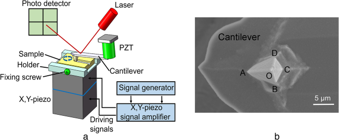
一 纳米铣削系统示意图。 b 金刚石涂层AFM针尖SEM显微照片
纳米通道和微通道模具的制造
PDMS 芯片上纳米通道的制造路线如图 2 所示。采用 AFM 系统和压电致动器在 PC 片上制造纳米通道模具(尺寸可控)。 15 mm×12 mm×1 mm的PC片材(分子量35000)购自Goodfellow。 PC板的表面粗糙度(Ra)的平均值和标准偏差分别测量为0.6 nm和0.2 nm(这些值是通过在AFM轻敲模式下扫描样品的50 μm×50 μm区域获得的)。为了产生圆周运动,压电致动器由在 x 和 y 方向上具有 90° 相位差的正弦信号驱动。加工后的纳米通道的宽度取决于产生的圆周运动的幅度。输入压电致动器的驱动电压范围设置为30 V到150 V,间隔为30 V,另外选择了100 Hz和1500 Hz两个驱动频率。在沿边缘向前的方向加工期间,材料以堆积的形式排出,并且经常被发现均匀分布在纳米通道的两侧 [45],这有助于避免在键合过程中纳米流体芯片的任何泄漏;因此,本研究选择了前向加工方向。使用 AFM 系统的 Nanoman 模块制造了 80-μm 长度的纳米通道。任何加工过程都受进给量的影响;因此,为了消除这种影响,进给速度应随驱动频率而变化。在本研究中,进给值设置为 10 nm,100 Hz 和 1500 Hz 频率的进给速率分别计算为 1 μm/s 和 15 μm/s。针尖的正常负载取决于位置敏感光电探测器 (PSD) 产生的输出电压;因此,我们研究中使用的不同正常负载是通过设置相对电压(设定点)来实现的。根据我们之前的工作[46],加工法向载荷由方程计算。 (1) 灵敏度由得到的力-距离曲线的斜率[47]测得。
$$ {F}_{\mathrm{N}}={V}_{\mathrm{setpoint}}\timessensitive\times {K}_{\mathrm{N}} $$ (1) <图片>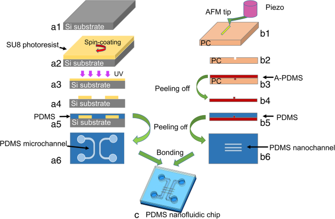
纳米流体芯片制造流程图:(a1)-(a6)PDMS芯片上微通道制造的工作步骤; (a1) 用于光刻基板的硅片; (a2) 在Si衬底上旋涂SU8光刻胶; (a3) SU8 层暴露在紫外光下; (a4) 获得凸状微结构; (a5) 微通道模具上的 PDMS 涂层; (a6) 带有微通道的最终 PDMS 芯片; (b1)-(b2) 在 PDMS 芯片上制造纳米通道的工作步骤; (b1) PC 板上的 AFM 尖端划痕; (b2) 划痕后得到纳米通道模具; (b3) 纳米通道模具上的 A-PDMS 涂层; (b4) 具有凸起纳米结构的 A-PDMS 芯片; (b5) A-PDMS 模具上的常规 PDMS 涂层; (b6) 具有纳米通道的最终 PDMS 芯片; (c) 键合后的PDMS纳米流体芯片
因此,纳米铣削过程的正常载荷设置为 17 μN 和 25 μN。此外,为了比较,PC片上的纳米通道模具也是在没有振动的情况下制造的,这种方法称为单刮。单次划痕过程的法向载荷设置为25 μN、33 μN、42 μN、50 μN和58 μN。纳米通道模具截面示意图如图2(b2)所示。
采用紫外光刻工艺制备微通道模具。图 2(a1-a4)中的流程图描述了光刻工艺的操作细节。将光刻胶(SU-82015;MicroChem,美国)以 500 rps 的速度旋涂在 Si 衬底上 30 s,并以 4000 rps 的速度旋涂 120 s。一对“U”形微通道形成微通道芯片(图2(a6)),通过纳米通道桥接形成最终的纳米流体芯片。微通道的宽度为30 μm,储液器的直径为1 mm。此外,两个“U”形微通道之间的距离为50 μm(附加文件1:图S1和S2)。
微通道和纳米通道的转移打印
通过PDMS(Sylgard 184,Dow Corining,USA)转移凸微通道模具(图2(a4))和凹面纳米通道模具(图2(b2))以制备最终的纳米流体芯片。图2(b3)-(b6)展示了纳米通道模具转移的工艺流程,包括两个步骤:第一次转移和第二次转移。为了研究单体与固化剂的重量比对纳米通道尺寸的影响,在第一次和第二次转移过程中采用了三种不同的 PDMS 重量比 (A-PDMS)。第一次转移印刷过程的 PDMS 重量比设置为 9:1、7:1 和 5:1,而第二次转移的值设置为 10:1、9:1 和 8:1。图 2(a5) 和 (a6) 显示了使用一步转移方法的微通道模具转移过程。 10:1的PDMS重量比用于凸微通道的转移。在所有转移印刷过程中,首先将双组分 PDMS 弹性体均匀搅拌,然后倒入外壳中以制备模具。然后将外壳在真空干燥器中保持 30 分钟,并脱气 2-3 次以去除所有捕获的气泡。将制备好的模具在80 °C的加热炉中保温4 h,最后将PDMS复制品从模具上轻轻剥离。
芯片键合
在1.5 毫巴的腔室压力和81 W的腔室功率下,通过氧等离子体处理(Zepto,Dienerelectronic,Germany)将制备的纳米流体芯片结合32 秒(图2(c))。微通道和纳米通道的表面用透明胶带清洁,在粘合前对 PDMS 微通道芯片上的四个水库进行冲压。等离子处理后,使用去离子水保持芯片清洁,并使用由支架、单目显微镜和一维精密载物台(TSDT-401S;SIGMAKOKI,日本)组成的自制对准系统将芯片保持对准。 ) (图 3a)。自制对准系统的详细信息可以在 ESI 中找到。然后将芯片在95 °C的温度下粘合20 分钟,以获得封闭的微/纳米通道芯片(图3b)。
<图片>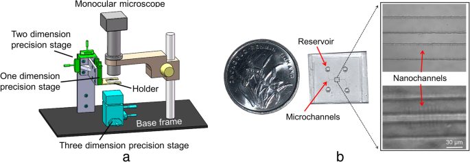
一 自制对中系统示意图及b 纳米流控芯片
结果与讨论
压电执行器的旋转轨迹
二维压电致动器是在基于 AFM 尖端的纳米铣削系统中进行旋转运动的关键部件。因此,为了表征其在一系列驱动电压和频率下的运动,进行了初步的划痕测试。在扫描范围为 0 nm 的接触模型下,AFM 尖端在给定的法向载荷下首先接近 PC 板的表面并保持静止。二维压电致动器的旋转由预设的频率和电压控制。完成划痕过程后,将 AFM 尖端从 PC 板表面抬起。因此,压电致动器的运动幅度作为驱动电压和频率的函数获得。驱动电压设置在 30-150 V 范围内,间隔为 30 V,而驱动频率设置为 100 Hz 和 1500 Hz。两个驱动频率下测量的幅度和驱动电压之间的关系显示在附加文件 1:图 S3 中。可以看出,随着驱动电压的增加,加工幅度值增大,1500 Hz时的加工幅度值大于100 Hz时的加工幅度值。发现通过我们提出的方法制造的纳米通道的宽度范围为350 nm到690 nm。
在 PC 板上制作纳米通道模具
单次划痕和纳米铣削下纳米通道尺寸与加工参数之间的关系分别如图 4a 和 b 所示。加工后的纳米通道的宽度和深度由 W 表示 0 和 D 0,分别为(图 5a)。
<图片>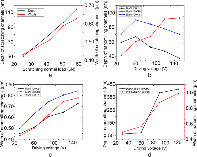
加工纳米通道尺寸与加工参数的关系:a 单次刮擦,正常负载范围从 25 μN 到 58 μN,b 深度和 c 在正常载荷为 17 μN、25 μN 和驱动频率为 100 Hz、150 Hz、d 的情况下制造的加工通道的宽度 正常载荷25 μN和驱动频率1500 Hz下加工通道的深度和宽度
<图片>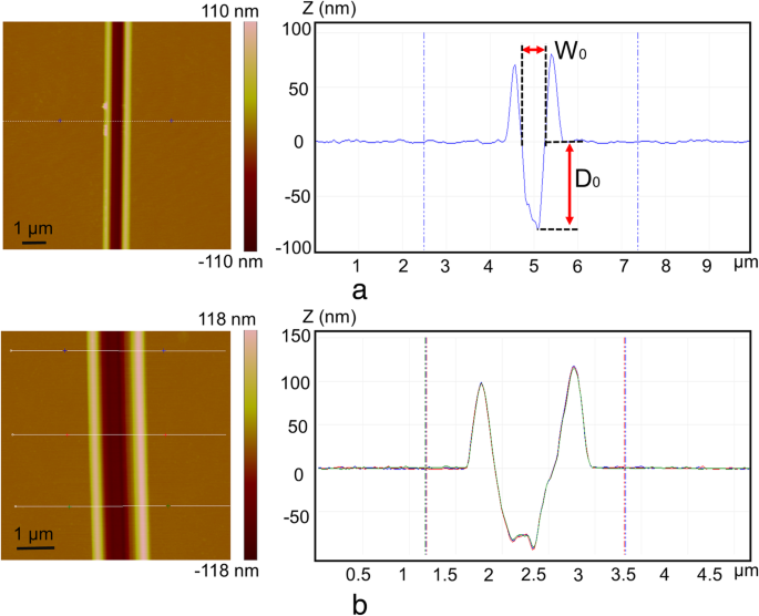
具有不同加工参数的加工纳米通道的典型 AFM 图像:a 在 42 μN 的正常负载下划伤。 b 正常负载25 μN、频率100 Hz、驱动电压60 V下的纳米铣削
从图 4a 可以看出,随着法向载荷的增加,所制造的纳米通道的宽度和深度也增加。在 42 μN 的正常载荷下划痕的典型 AFM 图像如图 5a 所示。值得注意的是,材料从纳米通道中排出,形成堆积物,均匀分布在纳米通道的两侧。因为 AFM 尖端的形状与加工过程中由边缘“OA”形成的表面对称(图 1b)。因此,在边缘向前刮擦期间,材料被尖端的前边缘均匀地排出。图 4b、c 和 d 说明了加工纳米通道尺寸与驱动电压之间的关系。从图 4b 可以明显看出,纳米通道的深度在开始时增加,然后在 100 Hz 的频率下开始减小,正常负载为 17 μN 和 25 μN。我们研究中使用的 PC 板是一种无定形聚合物,它在高应变水平下呈现出弹性-粘塑性与指数应变硬化相结合的行为 [48, 49]。加工过程中的法向载荷由方程计算。 (2) 其中\( \overrightarrow{n} \) 和\( \overrightarrow{t} \) 分别是流线向量的单位法线和单位切线,p 和 τ 分别表示局部法向压力和剪应力,\( \overrightarrow{z} \) 为垂直单位[50]。
$$ {F}_{\mathrm{N}}=p\cdot \int \overrightarrow{n}\cdot \overrightarrow{z} ds-\tau \cdot \int \overrightarrow{t}\cdot \overrightarrow{zds } $$ (2)在本研究中,所制造的纳米通道的尺寸尺寸为纳米级,因此假定局部法向压力和剪切应力的值是恒定的。此外,方程。 (2) 被转换成方程的简化形式。 (3),其中S n 和 S h 分别为AFM针尖与样品界面的水平投影和垂直投影。
$$ {F}_{\mathrm{N}}=p\cdot {S}_n-\tau \cdot {S}_h $$ (3)S之间的关系 n 和 S h 用公式表示。 (4),其中α 和 β 分别为端面与垂直面和水平面的夹角。
$$ {S}_{\mathrm{n}}=\frac{S_{\mathrm{h}}}{\cos \alpha}\cdot \cos \beta $$ (4)正常载荷由公式计算。 (5).
$$ {F}_{\mathrm{N}}=\left(p\cdot \frac{\cos \beta }{\cos \alpha }-\tau \right)\cdot {S}_h $$ (5 )从方程很明显。 (1) 在整个加工过程中法向载荷的值是恒定的。根据布里斯科等人的说法。 [51],平均应变率的值由方程计算。 (6),其中 V 和 w 分别表示刀尖速度和未切削切屑厚度。未切屑厚度的最大值为~ 10 nm。
$$ {}_{\varepsilon}^{\bullet }=\frac{\mathrm{d}\varepsilon }{\mathrm{d}t}\approx \frac{V}{w} $$ (6)此外,尖端速度的值是从方程中获得的。 (7),其中 f 是输入信号频率。
$$ V=\pi \cdot {W}_o\cdot f $$ (7)100 Hz下的平均应变率值在1.42×10 4 范围内 s -1 ~ 2.27 × 10 4 s -1 .局部正常压力值 (p ) 当应变率在 1.42 × 10 4 范围内时,随着应变率的增加而上升 s -1 到 2.27 × 10 4 s -1 [52]。 τ的值 远小于 p , 表示正常负载主要取决于 p .因此,为了保持正常负载的值(FN ) 在整个加工过程中保持不变,在较高的驱动电压下加工深度的值应该较小。然而,所制造的纳米通道的最终尺寸受样品材料回收率的影响。在 142~227 μm/s 的范围内,样品的回复率随着加工速度的增加而降低 [53]:因此,这表明在 30 V 下发生了更高的弹性回复。因此,在 30 V 下制造的纳米通道的深度(~142 μm/s) 比 60 V (~161 μm/s) 浅。附加文件 1:图 S4(a) 和图 5b 分别是在 17 μN 和 25 μN 的正常负载下以 100 Hz 加工的纳米通道的典型 AFM 图像。很明显,纳米通道右侧的堆积比左侧大。纳米铣削过程中样品的旋转运动为逆时针方向,主切削刃的切削角度随着旋转而变化。未切割的切屑厚度太小,无法在纳米铣削工艺循环的开始和结束时形成切屑。纳米铣削过程中间的未切削切屑厚度较大;然而,小的攻角有助于形成堆积。因此,更多的材料被推到通道的右侧,堆积因此不对称。 不对称堆积形成的细节可以在我们之前的研究中找到[54]。
从图 4b 和 d 可以看出,在 17 μN 和 25 μN 的正常负载下,纳米通道的深度随着 1500 Hz 的驱动电压的增加而开始增加。图 4d 描绘了在 25 μN 的正常负载下,纳米通道深度从 60 V(~ 2.64 mm/s)急剧增加到 90 V(~ 4.10 mm/s)。根据耿等人的说法。 [55],切削速度显着影响材料去除状态。材料在加工过程中以 2.64 mm/s 的速度以堆积的形式从纳米通道中排出,而材料去除状态以 4.10 mm/s 的速度从堆积变为切屑(附加文件 1:图 S4(b)) .因此,在 90 V (~4.10 mm/s) 时加工深度的增加可归因于材料去除状态的变化。随着驱动电压的增加,制备的纳米通道的宽度开始增加。图6为纳米铣削过程中AFM针尖轨迹示意图,虚线椭圆、黑色实心椭圆、蓝色箭头分别代表加工完成、正在进行的加工和AFM针尖的运动方向。宽度 (W 2) 图 6(b) 中的加工通道大于 (W 1) 在图 6(a)。 AS1 和 AS2(红色实线)代表 AFM 尖端和样品材料的横截面之间的接触长度。当加工宽度为“L”时,发现AS1的值大于AS2的值 1”等于“L 2.”
<图片>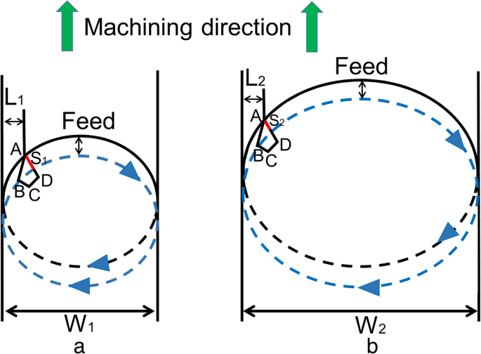
纳米铣削过程中 AFM 尖端轨迹的示意图:纳米通道的加工宽度 (a ) 小于纳米通道 (b ),虚线椭圆、黑色实心椭圆和蓝色箭头分别表示加工完成、正在进行加工和AFM针尖的运动方向
Sh 的值 在方程式中(5) 由方程获得。 (8) 其中D和AS分别是加工通道的深度和AFM尖端横截面与样品材料之间的接触长度。
$$ {S}_h=\frac{1}{2}\cdot \left|D\left|\cdot \right|\; AS\右| $$ (8)因此,方程。 (5) 被进一步改写为等式。 (9).
$$ {F}_{\mathrm{N}}=\frac{1}{2}\cdot \left(p\cdot \frac{\cos \beta }{\cos \alpha }-\tau \right) \cdot \left|D\left|\cdot \right| AS\右| $$ (9)α 的值 和 β 在整个加工过程中保持恒定。 1500 Hz 处的应变率值在 2.03 × 10 5 范围内 ~3.66 × 10 5 s -1 ;因此,可以假设局部正常压力 (p ) 在 1500 Hz 时达到其极限值。此外,加工速度在 30-150 V(~ 2.03-3.66 mm/s)下加工期间对样品的恢复没有影响[53];因此,纳米通道的最终尺寸仅由加工尺寸决定。对于较大的加工宽度,发现 AS2(图 6(b))的值小于 AS1(图 6(a))的值,并且根据等式。 (9) 中,AS 值越小,D 值越大。因此,加工深度的值随着驱动电压的增加而增加。在 25 μN 的正常负载、120 V 的驱动电压和 1500 Hz 的频率下制造的纳米通道的典型 AFM 图像显示在附加文件 1:图 S4(b) 中。值得注意的是,材料在芯片和堆积形成中都被去除,并且排出的材料仅在纳米通道的一侧积累。此外,在 25 μN 的正常负载下,在 150 V 的电压下加工时,排出的材料在纳米通道底部的切屑形成中积累。因此,在电压为 150 V 和频率为 1500 Hz(在正常负载为 25 μN 下)加工期间制造的纳米通道的尺寸数据在图 4d 中为空。
从图 4c 中可以明显看出,随着驱动电压的增加,纳米通道宽度开始增加。此外,当正常负载和驱动电压值保持恒定时,1500 Hz频率下制备的纳米通道宽度比100 Hz宽。此外,在 1500 Hz 下制造的纳米通道的加工深度比 100 Hz 的加工深度更深,并且发现在加工更深的纳米通道期间尖端的横截面尺寸更大。因此,当加工更深时,纳米通道制造得更宽。
纳米通道模具的第一次转移
在 25 μN、33 μN、41 μN、50 μN 和 58 μN 的正常载荷下通过单次划痕方法加工的纳米通道应用于第一次转移过程。此外,在30-150 V的驱动电压范围内(间距为30 V),在100 Hz的频率下通过纳米铣削制造的纳米通道模具也用于转移过程。通过单次划痕方法加工的纳米通道(80 nm深度和510 nm宽度)被称为“纳米通道I”,而通过纳米铣削制造的纳米通道(50 nm深度和610 nm宽度,90 nm深度和630 nm宽度)被称为“纳米通道” II”和“纳米通道 III”。在第一次转移过程中使用了三种不同的PDMS重量比(5:1、7:1和9:1)。
图 7a 和 b 揭示了在正常负载 25 μN 和频率 100 Hz 下,不同 PDMS 重量比对壁尺寸的影响,黑色虚线表示转移前的原始纳米通道尺寸。图 7c 和 d 中显示了在第一次转移过程中以 5:1 的重量比从纳米通道 III 获得的壁的典型 AFM 图像和相应的横截面,该壁被称为“壁 III”。在 ESI 中显示了在 17 μN 法向载荷和 100 Hz 频率下单次刮擦过程中不同 PDMS 重量比对壁尺寸的影响(参见附加文件 1:ESI 的图 S5、S6、S7 和 S8详情)。从“纳米通道 I”和“纳米通道 II”获得的壁分别称为“壁 I”和“壁 II”。很明显,不同 PDMS 重量比的所有墙壁的高度大致相同。 The widths of the walls were larger than the original nanochannel width, and the width at the weight ratio of 5:1 was found to be the largest. Due to the thermal expansion of PC sheet, a small deviation was noticed between final wall size and original nanochannel size. It was also observed that the elasticity of PDMS increased as the PDMS weight ratio decreased from 5:1 to 7:1 [41, 42]. Hence, the wall obtained at the weight ratio of 5:1 was stiffer and its elastic recovery was smaller; thus, the width of the wall obtained at the weight ratio of 5:1 was the largest.

Relationship between a wall height, b wall width, and transfer parameters (various weight ratio of PDMS) during first transfer process, where the channel molds were fabricated with a normal load of 25 μN and a frequency of 100 Hz, and c typical AFM image and d corresponding cross-section of the wall obtained from nanochannel III at a weight ratio of 5:1
Second transfer of nanochannel molds
The final PDMS slabs with nanochannels were obtained during second transfer process based on the wall obtained at a weight ratio of 5:1 in the first transfer process. Three different PDMS weight ratios (10:1, 9:1, and 8:1) were used during second transfer process. Figure 8a and b present the relationship between nanochannel size obtained under a normal load of 25 μN and a frequency of 100 Hz and transfer parameters during second transfer. It is clear from Fig. 8a that the depths of the nanochannels were larger than the original machining size, moreover, the depth at 10:1 was found to be larger than other two ratios. Further, the widths of the wall were also larger than the original size, and the width at 10:1 was found to be the largest (Fig. 8b). Figure 8c and d present a typical AFM image and corresponding cross-section of the nanochannel (120 nm depth and 690 nm width) obtained from wall III at a weight ratio of 10:1 during second transfer, and it was termed as “nanochannel C.” The relationship between the nanochannel sizes obtained under single scratching process with a normal load of 25 μN and a frequency of 100 Hz and the transfer parameters during the second transfer process were shown in ESI (see Additional file 1:Figures. S9, S10, S11 and S12 of ESI for details), the nanochannels obtained from “wall I” and “wall II” were termed as “nanochannel A” and “nanochannel B”, respectively.

Relationship between a nanochannel height, b nanochannel width, and transfer parameters (various weight ratio of PDMS) during second transfer, where the channel molds were fabricated with a normal load of 25 μN and a frequency of 100 Hz, and c typical AFM image and d corresponding cross-section of the nanochannel obtained from wall III at a weight ratio of 10:1 during second transfer
The depths of nanochannels obtained from walls II and III were larger than the original machining size, whereas the depth obtained from wall I was smaller than the initial machining size. Furthermore, the changes in width were identical to the changes in depth. The aspect ratio of wall I was larger than those of walls II and III, thus each wall manifested different thermal expansion values. Hence, the changing trends of width and depth during second transfer were different though at the same PDMS weight ratio. The values of the depth and width of walls II and III at 9:1 and 8:1 were found to be closer to the original machining size compared with 10:1. Because the elastic recoveries of PDMS at 9:1and 8:1 are closer to 5:1 than 10:1, which indicates an almost similar recovery trend for PDMS at 9:1, 8:1, and 5:1.
Application of nanochannel devices in electric current measurement
Nanochannel devices are often used in the fields of single nanoparticle manipulation, electrokinetic transport phenomena, DNA analysis, and enzymatic reaction detection. The main working principle of nanofluidic chips depends on the variation in electric current; therefore, it is important to measure the electrical conductivities of nanochannel devices. The electrical conductance in a nanochannel can be estimated by Eq. (10) [56].
$$ G={10}^3N\;{}_Ae\frac{wh}{l}\sum {\mu}_i{c}_i+2{\mu}_e\frac{w}{l}{\delta}_n $$ (10)其中 μ 我 is the mobility of ion i , c 我 is the concentration of ion i , δ n is the effective surface charge inside the nanochannel, and NA and e signify Avogadro constant and electron charge, besides, w , h 和 l are the nanochannel width, height and length, respectively. It is obvious that the electrical conductance of a nanochannel is affected by the nanochannel feature dimensions and the solution concentration. The electric double layer (EDL) plays an important role in the nanochannel when the ratio of DEL thickness to the nanochannel height increases. The diffuse layer thickness of EDL is 3~5 times of the Debye length (λ D ), which can be expressed by Eq. (11) [57].
$$ {\lambda}_D=\sqrt{\frac{\varepsilon_0{\varepsilon}_r{k}_bT}{2{n}_{i\infty }{(ze)}^2}} $$ (11)其中 n 我 ∞ denotes ion density in the solution, ε o is the permittivity of vacuum, ε r is the dielectric constant of electrolyte solution, z is the valency of buffer solution (z = z + − z - = 1 for KCl), and kb 和 T are the Boltzmann constant and temperature, respectively. In the present study, three different nanofluidic chips were obtained after the completion of transfer process. Nanofluidic chips consisted of nanochannels A, B, and C were termed as nanofluidic chips A, B, and C, respectively. Each nanofluidic chip contained four nanochannels. The widths and the depths of nanofluidic chips A, B, and C were measured as 60 nm and 500 nm, 80 nm and 680 nm, and 120 nm and 690 nm, respectively. The effective length of nanochannels in all chips was calculated as 50 μm. As shown in Fig. 8, pile-ups distribute on the sides of the nanochannels A, B, and C. The pile-ups may fill into the nanochannels and lead to a failure of the preparation for the nanofluidic chips. Thus, in order to verify the reliability of the fabricated nanochannel devices, electrical conductivity measurement test was conducted. KCl with 1 mM concentration was as the electrolyte solution in our study, and the values of electrical current were measured by an electrometer (Model 6430, Keithley, USA). The schematic sketches of the measurements for electric current in microchannel and nanochannel are presented as the inset figures in Fig. 9a and b, respectively. The experiments were carried out under DC power (applied by an Ag electrode) with an increment of 2 V for 3-s duration. Figure 9a presents the measured I -V curves of microchannels in three different nanofluidic chips, and a linear relationship between current and voltage was observed. Moreover, as the effect of EDL in microchannels was negligible and the dimensional sizes of microchannels in different nanofluidic devices were identical, the values of current in different chips were nearly the same. It is evident from Fig. 9b that the values of current in different nanofluidic devices were distinct due to different nanochannel sizes. For KCl solution of 1 mM concentration, the value of λ D was about 10 nm, thus the diffuse layer thickness of EDL was found as 30~50 nm [57]. Consequently, EDL got overlapped along the depth (60 nm) of nanofluidic chip A; however, no overlapping was observed in nanofluidic chip C (depth of 120 nm). However, it was difficult to determine whether EDL got overlapped or not in nanofluidic chip B (depth of 80 nm). It assumes that the effective surface charges (δ n ) in all nanochannels are identical as the charge density of a surface is material property [58, 59]. The concentration of the ions in a nanochannel depends on the EDL field, the stronger the EDL field, the higher the ion concentration in the nanochanel [44]. In the present study, the EDL field in nanofluidic chip A is the strongest as the highest ratio of the DEL thickness to the nanochannel height, which signifies that the ion concentration in the nanochannel of nanofluidic chip A is the highest.根据方程。 (10), the nanochannel of nanofluidic chip A is more conductive due to the higher ion concentration. Hence, the value of electrical current in nanofluidic chip A was the largest, whereas nanofluidic chip C yielded the smallest value. In addition, at larger width sizes, EDLs did not overlap along the width directions of nanochannels. In nanofluidic chip B, when the value of applied electric field was lower than 25 V, a linear relationship was noticed between current and applied voltage; however, a limiting region appeared as the value of applied voltage increased and finally, became liner again as the electrical field increased further, this phenomenon belongs to ohmic-limiting-overlimiting current characteristic [60, 61]. The results of electrical current measurement revealed that the nanofluidic devices fabricated by the proposed method were effective, the pile-ups of the nanochannels A, B, and C had almost no influence on the performance of the nanofluidic devices.

Electric current measurement results based on the fabricated nanochannel devices, the cross-section size (depth × width) of nanochannels for nanofluidic chip A, B, and C are 60 × 500 nm, 80 × 680 nm and 120 × 690 nm, respectively. 一 Current in microchannels. b Current in nanochannels. The insets display the schematic sketches of the measurements
结论
In the present research, nanochannels with controllable sizes (sub-100-nm depth) were fabricated by AFM tip-based nanomilling, and for the first time, the machined nanochannels were applied to prepare nanofluidic devices. The multichannel nanofluidic devices were prepared in four steps:(1) fabrication of nanochannels by AFM tip and piezoelectric actuator, (2) fabrication of microchannels by lithography, (3) transfer of micro- and nanochannels, and (iv) bonding. Further, nanochannel sizes were controlled by changing the driving voltages and frequencies inputted to the actuator. The heights of the wall obtained during first transfer were smaller than the original machining size, whereas the widths were larger than the original machining size. The experiment results revealed that during second transfer process, nanochannel sizes affected PDMS weight ratios. Finally, micro-nanofluidic chips with three different nanochannel sizes were obtained by bonding a PDMS nanochannel chip on a PDMS microchannel chip. Moreover, the electrical current measurement experiment was conducted on the fabricated nanofluidic chips, and it was found that the values of current were affected by nanochannel sizes. Therefore, PDMS nanofluidic devices with multiple nanochannels of sub-100-nm depth can be efficiently and economically fabricated by the proposed method.
Compared with other fabrication approach, the proposed method for fabrication of the nanofluidic devices in the study is easy to use and low cost; besides, the nanochannels with controllable dimension size can be obtained easily. However, the commercial AFM system cannot equip with a large-scale high-precision stage due to the spatial limitation; thus, the maximum fabrication length of the nanochannel is confined as 80 μm. In addition, the tip wear cannot be neglected after long-term fabrication due to the high machining speed, which should be investigated in future work.
缩写
- 原子力显微镜:
-
原子力显微镜
- DC:
-
直流电
- EDL:
-
Electric double layer
- KCL:
-
Potassium chloride
- PC:
-
Polycarbonate
- PDMS:
-
聚二甲基硅氧烷
- PSD:
-
Position-sensitive photodetector
纳米材料