

二维自旋电子学的最新进展
摘要
自旋电子学是开发替代多功能、高速、低能量电子设备的最有前途的技术。由于其不寻常的物理特性,新兴的二维 (2D) 材料为探索新型自旋电子器件提供了新平台。近年来,二维自旋电子学在理论和实验研究方面都取得了很大进展。在这里,回顾了二维自旋电子学的进展。最后指出了该领域当前面临的挑战和未来的机遇。
介绍
随着巨磁阻效应(GMR)的发现和应用,自旋电子学迅速发展成为一个有吸引力的领域,旨在利用电子的自旋自由度作为信息载体来实现数据存储和逻辑运算[1,2,3 ]。与传统的基于电荷的微电子器件相比,自旋电子器件需要更少的能量来切换自旋状态,从而可以实现更快的运行速度和更低的能耗。因此,自旋电子学是开发替代的多功能、高速、低能量电子设备的最有前途的技术。尽管自旋转移矩磁阻随机存取存储器(STT-MRAM)已经实现商业化生产,但仍有各种技术问题需要解决。主要挑战包括自旋极化载流子的有效产生和注入、自旋的长距离传输以及自旋方向的操纵和检测[4,5,6]。
在自旋电子学的蓬勃发展的同时,二维 (2D) 范德华 (vdW) 材料自石墨烯分离以来一直处于材料研究的前沿 [7,8,9]。与散装材料不同,2D vdW 材料表现出许多新颖的物理现象。一些 2D 材料已经在下一代 2D 自旋电子器件的工程设计中显示出巨大的潜力 [10,11,12]。例如,石墨烯表现出高电子/空穴迁移率、长自旋寿命和长扩散长度,这使其成为自旋通道的有希望的候选者 [13,14,15]。然而,由于其零间隙和弱自旋轨道耦合 (SOC) 的特性,石墨烯在构建基于石墨烯的电流开关方面存在局限性。相比之下,二维过渡金属二硫属化物 (TMDC) 具有不同的带隙、强大的 SOC 效应,尤其是独特的自旋谷耦合,为非易失性信息存储提供了一个操纵自旋和谷自由度的平台 [16, 17]。具有拓扑保护表面状态的拓扑绝缘体 (TI) 具有很强的自旋轨道相互作用以实现自旋动量锁定,这可以抑制散射并提高自旋和电荷转换效率 [4, 12, 18]。具有低至原子层厚度的固有磁性基态的新兴二维磁体为新型二维自旋电子应用开辟了新途径 [19,20,21]。
随着二维自旋电子学的发展,有必要回顾该领域最新的实验和理论工作。本文回顾了二维自旋电子学的进展,也讨论了这个新兴领域目前面临的一些挑战和未来的机遇。第一部分回顾了 2D 材料中的磁性,包括石墨烯、TI 和其他一些通过掺杂或邻近效应方法的 2D 材料中的感应磁矩,以及一些本征 2D 磁体。第二部分介绍了实现二维自旋电子器件操作的三个基本功能,包括二维材料及其界面中的自旋电荷转换、自旋输运和自旋操纵。第三部分概述了二维自旋电子学的应用。第四部分介绍了几种用于存储器存储和逻辑应用的潜在 2D 自旋电子器件。最后一部分讨论了二维自旋电子学实现实际应用的一些当前挑战和未来机遇。
二维材料中的磁性
磁性在数据存储技术中具有重要意义。然而,像石墨烯这样的大多数二维材料本质上都不是磁性的。已经提出了两种使非磁性材料具有磁性的方法。第一种方法是通过引入空位或添加吸附原子来产生自旋极化 [22,23,24]。另一种是通过与相邻磁性材料的磁邻近效应引入磁性 [18, 25, 26]。最近发现的二维磁性vdW晶体在原子尺度上具有固有的磁性基态,为自旋电子学领域提供了前所未有的机遇[20, 27]。
石墨烯中的感应磁矩
原始石墨烯具有很强的抗磁性,因此大量的理论和实验研究探索了石墨烯的磁性。引入空位和添加氢或氟已被用于在石墨烯中诱导磁矩 [23, 25, 28]。例如,Kawakami 的团队利用氢吸附原子掺杂石墨烯(图 1a),并通过非局部自旋输运测量检测纯自旋电流,以证明石墨烯中的磁矩形成 [23]。如图 1b 所示,非局域自旋输运测量中出现在零磁场处的特征倾角表明,纯自旋电流通过传导电子与局域氢感应磁矩之间的交换耦合而散射。此外,具有氟吸附原子和空位缺陷的石墨烯具有顺磁矩,可以通过 SQUID(超导量子干涉装置)进行测量 [28]。尽管如此,在掺杂石墨烯中实现长程铁磁有序仍然是一个巨大的挑战。一些研究人员提出利用磁邻近效应使石墨烯获得磁性[29]。当石墨烯与磁性绝缘体相邻时,石墨烯的 π 轨道与磁性绝缘体中相邻的自旋极化 d 轨道发生交换相互作用,产生长程铁磁耦合。如图1c所示,在石墨烯/钇铁石榴石(YIG)异质结构中,测得的异常霍尔效应信号可以持续到250 K(图1d)[25]。
<图片>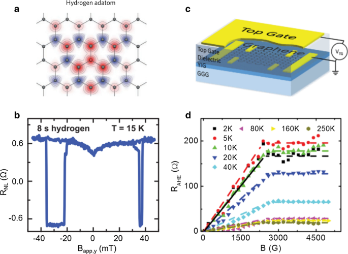
经 McCreary 等人许可转载,物理。牧师莱特。 109, 186,604 (2012)。版权所有 2012 美国化学学会 [23]。 (c) 和 (d) 经 Wang 等人许可转载,Phys.牧师莱特。 114, 016,603 (2015)。版权所有 2015 美国化学会 [25]
石墨烯中的感应磁矩。 一 石墨烯中氢磁矩的理论预测。 b 在 15 K 时通过自旋输运测量检测到由于氢掺杂引起的磁矩。该器件是在 8 秒氢掺杂后测量的。 c 石墨烯交换耦合到原子级平坦的钇铁石榴石 (YIG) 铁磁薄膜的示意图。 d 磁性石墨烯在不同温度下的异常霍尔电阻测量。 一 , b
TI 中的感应磁矩
二维材料容易受到环境条件的影响,例如水分和氧气。 TI 表面区域的导电表面状态被认为是更稳定的二维材料 [30]。此外,TI 的表面态表现出自旋动量锁定特性,这提供了一种通过电荷电流方向操纵自旋信号的方法。更有趣的是,通过掺杂磁性原子或磁性邻近效应打破时间反转对称性会产生一些奇异的现象,例如量子反常霍尔效应 (QAHE) [18, 31]。张等人。 [24]首先在Cr掺杂的磁性TI中观察到QAHE,Cr0.15(Bi0.1Sb0.9)1.85Te3。如图 2a 所示,通过调整磁感应 TI 带的费米能级,我们可以观察到 e 的霍尔电导平台 2 /h .测量结果表明栅极可调异常霍尔电阻达到了h的量化值 /e 2 在零磁场(图 2b)。然而,掺杂磁性原子的自旋散射效应受限于在 TI 表面实现稳健的长程磁性有序。 TI与磁性材料之间的磁性接近可以避免掺杂原子或缺陷的引入,通过界面交换耦合获得长程磁性有序。自旋极化中子反射率 (PNR) 用于研究 Bi2Se3/EuS 异质结构处的界面磁性(图 2c)[32]。 PNR 结果表明 Bi2Se3/EuS 双层在界面处具有铁磁有序,这种拓扑增强的界面铁磁性可以持续到室温(图 2d)。预计在 TI 中实现铁磁表面状态将允许出现几种突出的现象,例如界面磁电效应 [33] 和电场诱导的图像磁单极子 [34]。
<图片>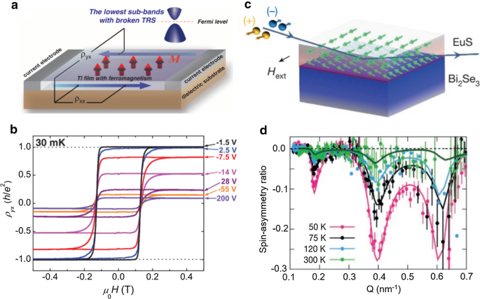
经 Chang 等人许可转载,Science 340, 167 (2013) )。版权所有 2013 美国科学促进会 [24]。 c, d 经 Katmis 等人许可转载,Nature 553, 513 (2016)。版权所有 2016 自然出版集团 [32]
TI 中的感应磁矩。 一 磁性 TI 薄膜中的 QAHE 示意图。磁化方向 (M) 由红色箭头表示。薄膜的化学势可以通过施加在介电基板背面的栅极电压来控制。 b 在 Cr0.15(Bi0.1Sb0.9)1.85Te3 薄膜中,QAHE 在不同栅极电压下的磁场依赖性。 c Bi2Se3/EuS 双层膜的偏振中子反射率 (PNR) 实验示意图。 d 通过 PNR 测量测量的 EuS 磁邻近耦合观察 Bi2Se3/EuS 双层样品中的铁磁有序。 一 , b
其他二维材料中的感应磁性
除了石墨烯和 TI 外,其他二维材料中由本征缺陷和掺杂剂引起的磁性也得到了研究,包括磷烯 [35]、硅烯 [36, 37]、GaSe [38]、GaN [39]、ZnO [40] 等. 第一性原理计算结果表明,空位和外部应变之间的相互作用可以在磷烯中产生磁性。当应变沿磷烯的Z字形方向且P空位达到4%时,系统呈现自旋极化状态,磁矩为 ~ 1 μ B 每个空置站点 [35]。第一性原理计算还预测,由于价带顶部电子态的交换分裂,空穴掺杂可以在 GaSe 和 GaS 中引起铁磁相变。磁矩可达1.0 μ B 每个载体 [38, 39]。然而,大多数这些研究仅限于理论计算。需要进一步的研究,特别是实验工作来了解磁性行为并探索用于实际应用的稳健二维室温铁磁半导体。
内部二维磁铁
最近,通过实验获得了 2D vdW 家族的另一个成员,即 2D 磁铁 [19, 41]。这一突破立即引起了人们对二维磁学领域探索的广泛关注。 Xu的团队首先报道了通过磁光克尔效应(MOKE)技术(图3a)[42],直到单层的CrI3表现出具有强烈面外磁各向异性的Ising铁磁性。此外,CrI3 表现出依赖于层的磁性相,其中单层和三层 CrI3 是铁磁性的,而双层是反铁磁性的。龚等人。报道了另一种二维材料 Cr2Ge2Te6,它在原子层中具有固有的长程铁磁有序 [43]。与 CrI3 不同,据报道 Cr2Ge2Te6 是一种具有小磁各向异性的二维海森堡铁磁体。如图 3b 所示,Cr2Ge2Te6 的铁磁转变温度与层数有关。另一种流行的二维铁磁体是 Fe3GeTe2,它是一种 vdW 铁磁金属,由层状 Fe/FeGe/Fe 组成,夹在两个 Te 原子层之间 [44]。反常霍尔效应已被用于研究 Fe3GeTe2 的磁性,结果表明 Fe3GeTe2 具有强磁各向异性,易磁化方向平行于 c 轴,居里温度为 230 K(图 3c)[45]。然而,这些材料的居里温度低于室温,是器件应用的一大障碍。居里温度高于室温是二维磁性材料实际应用的先决条件。研究人员通过分子束外延 (MBE) [41] 制备了室温铁磁单层 1 T-VSe2。最近报道的少层 1 T-CrTe2 的居里温度高达 316 K [46],这为未来二维自旋电子器件的应用提供了可能性。除了二维铁磁材料,二维反铁磁材料也被广泛报道,如 FePS3 [47]、MnPS3 [48] 和 CrCl3 [49]。更令人惊讶的是,张元博团队最近报道了一种内在磁性拓扑绝缘体 MnBi2Te4 中的磁场诱导 QAHE [50]。 MnBi2Te4是一种具有层内铁磁性和层间反铁磁性的反铁磁体。通过探测量子传输,在高于 μ 的中等磁场下观察到原始五层 MnBi2Te4 薄片中反常霍尔效应的精确量子化 0H 低温下~ 6 T(图3d)。
<图片>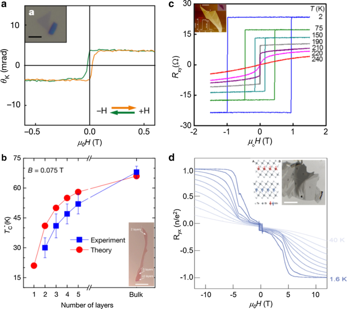
经黄等人许可转载,Nature 546, 271 (2017) )。版权所有 2017 自然出版集团 [42]。 b 经龚等人许可转载,Nature 546, 265 (2017)。版权所有 2017 自然出版集团 [43]。 c 经 Fei 等人许可转载,Nat。母校。 17, 778 (2018)。版权所有 2018 自然出版集团 [44]。 d 经 Deng 等人许可转载,Science 367, 895 (2020)。版权所有 2020 美国科学促进会 [50]
内在 2D 磁铁。 一 CrI3 单层的极性磁光克尔效应 (MOKE) 信号。插图显示了孤立的单层 CrI3 的光学图像。 b 不同厚度的 Cr2Ge2Te6 的转变温度 TC*,蓝色方块图来自克尔测量,红色圆圈图来自理论计算。插图显示了 SiO2/Si 上剥落的 Cr2Ge2Te6 原子层的光学图像。 c 在 12 纳米厚的 Fe3GeTe2 器件上测量的霍尔电阻的温度相关磁场扫描。插图显示了 SiO2 上具有代表性的 FGT 薄片的原子力显微镜图像。 d 五层 MnBi2Te4 样品中的磁场诱导 QAHE。与磁场相关的 R yx 在各种温度下。插图显示了 MnBi2Te4 的晶体结构和通过 Al2O3 辅助剥离方法裂解的 MnBi2Te4 的几层薄片的光学图像。 一
二维自旋电子设备操作的基本功能
新兴 2D 材料和一些先进表征技术的最新发展使 2D 自旋电子学领域迅速发展 [51,52,53]。实现自旋电子器件的关键问题包括自旋电荷转换、自旋输运和自旋操纵。自旋电流的有效产生和检测是开发替代电子自旋电子器件的二维自旋电子器件的主要挑战。自旋传输需要具有长自旋寿命和长距离自旋传播的合适传输通道。需要通过自旋操作来控制自旋电流并实现器件功能。
自旋电荷转换
提出了许多方法来实现自旋到电荷的转换,例如通过电自旋注入/检测或通过利用源自 SOC [54,55,56] 的自旋霍尔效应和 Edelstein 效应。然而,自旋霍尔效应通常发生在大块材料中,而埃德尔斯坦效应通常被认为是一种界面效应[55]。
“非局部”和“局部”测量通常用于对通道材料进行电自旋注入/检测[14]。对于非局部测量(图 4a),电极 E2 是作为自旋注入器的铁磁金属,而 E3 是作为自旋检测器的铁磁电极。施加的电流从电极 E1 流向 E2,E3 和 E4 用于检测扩散的纯自旋电流信号。 E3 和 E4 之间测量电压的极性取决于电极 E2 和 E3 的磁化配置。这种方法可以在没有充电电流的情况下获得纯自旋电流,而“局部”测量得到自旋电流和充电电流的混合信号(图 4b)。将电极E2和E3平行和反平行磁化排列之间的电压差视为自旋输运信号。
<图片>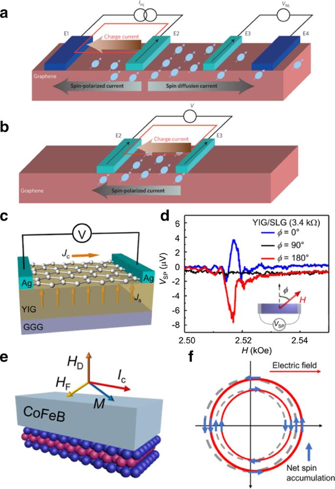
经 Han 等人许可转载,Nat。纳米技术。 9, 794 (2014)。版权所有 2018 自然出版集团 [14]。 c , d 经门德斯等人许可转载,物理。牧师莱特。 115, 226601 (2015)。版权所有 2015 美国化学学会 [68]。 e , f 经 Shao 等人许可转载,Nano Lett。 16, 7514 (2016)。版权所有 2016 美国化学会 [71]
二维材料中的自旋和电荷转换。 一 使用非局部测量几何结构进行电自旋注入和检测。 b 具有局部测量几何形状的电自旋注入和检测。 c YIG(铁磁绝缘体)上石墨烯中的自旋电荷转换。自旋电流由 YIG 的自旋泵浦产生,并转换为石墨烯中的充电电流。 d 在 YIG/石墨烯上测量的自旋泵浦电压的磁场依赖性 e MX2/CoFeB 双层的 SOT 测量。 MX2 代表 MoS2 和 WSe2。 f 在外部电场下,MX2/CoFeB 界面处 Rashba-Edelstein 效应(REE)诱导自旋积累的图示。 一 , b
希尔等人。首次报道了使用软磁性 NiFe 电极将自旋注入石墨烯 [57]。然而,自旋注入效率估计相对较低,约为 10%,这可能归因于铁磁金属和石墨烯之间的电导不匹配。然后,一些研究人员提出使用绝缘阻挡层(例如 Al2O3 或 MgO)作为调整界面自旋相关电阻率并提高自旋注入效率的层 [58,59,60],但生长高质量的氧化物层是主要的挑战。一些方法已被用于改进氧化物层生长技术或改变为另一个界面氧化物层,例如一层 TiO2 或 HfO2 [61, 62]。然而,界面自旋相关电阻率仍然是根本问题,这导致自旋注入效率低。一种二维绝缘材料六方氮化硼 (h-BN) 具有类似于石墨烯的晶体结构。理论和实验研究表明,使用h-BN作为隧道势垒可以产生高质量的界面,大大提高石墨烯的自旋注入效率。少层 h-BN 表现出比单层 h-BN 更好的自旋注入性能 [63, 64]。尽管如此,这些研究成果在实际应用之前仍有很大的空白有待填补。最终,要实现完美的(100%)自旋注入需要大量研究,而二维材料提供了一个有前景的方向,例如由二维铁磁材料、二维隧道势垒和二维传输通道组成的二维异质结构。
(逆)Rashba-Edelstein 效应是源自强 SOC 的界面效应,可用于实现自旋电荷转换 [65]。虽然本征石墨烯的 SOC 相当弱,但它可以通过邻近效应利用相邻材料的强 SOC 实现高效的自旋电荷转换 [66, 67]。如图 4c 所示,当石墨烯与铁磁绝缘体 YIG 相邻时,通过自旋泵浦在 YIG 层中产生自旋电流,然后通过逆埃德尔斯坦效应将自旋电流转换为石墨烯中的充电电流 [68]。图 4d 显示了作为 YIG/石墨烯器件中场的函数的自旋泵浦电压曲线。可以在垂直于石墨烯通道的磁场中检测自旋泵浦电压。此外,当外部磁场沿石墨烯通道转动时,没有自旋泵浦电压。此外,石墨烯表面的离子液体门控可以明显调节石墨烯的性质,从而改变YIG/石墨烯的自旋电荷转换效率[56]。
与石墨烯不同,具有强 SOC 的 TMDC 被认为是实现自旋电荷转换的有前途的材料 [69, 70]。单层TMDC(MoS2或WSe2)/CoFeB双层结构中的大自旋轨道扭矩(SOT)是通过由Rashba-Edelstein效应引起的电流诱导自旋积累产生的(图4e,f)[71]。类场转矩和类阻尼转矩是通过二次谐波测量确定的,结果表明大面积单层 TMDCs 由于其磁化反转效率高而具有潜在的应用。此外,自旋扭矩铁磁共振 (ST-FMR) 技术已用于研究 TMDC 中的自旋和电荷转换。例如,一个有趣的 ST-FMR 结果表明 SOT 可以通过 WTe2/坡莫合金双层中 WTe2 的晶体对称性来控制。当沿 WTe2 的低对称轴施加电流时,可以产生平面外反阻尼扭矩 [72]。 TI 表面态的自旋动量锁定特性有助于通过 SOT 实现自旋电流注入相邻材料。由于自旋极化方向和电荷电流方向之间的强相关性,自旋方向可以通过 TI 中的电荷电流来操纵。不同的测量技术已被用于研究自旋电荷转换,包括二次谐波测量、自旋泵浦和 ST-FMR。这些测量结果表明在二维材料如TMDCs和TIs中产生高效的SOT是可能的。
旋转传输
自旋输运的关键是获得一个有利的自旋输运通道,具有长的自旋扩散长度和自旋弛豫时间。自旋弛豫是由动量散射引起的,因此具有弱 SOC 的石墨烯被认为是自旋输运的理想材料 [14, 73]。汤布罗斯等人。 [74]在2007年通过非局域测量在室温下在横向单石墨烯自旋阀中实现了电子自旋输运和自旋进动。 如图5a,b所示,非局域自旋阀由四端铁磁钴作为电极组成,薄的 Al2O3 氧化物层作为阻挡层,石墨烯片作为自旋传输通道。图 5c 中的测量信号表明,如果用于自旋注入和自旋检测的铁磁电极具有平行磁化,则触点 1 和 2 测量的非局部电阻具有正值。如果用于自旋注入和自旋检测的铁磁电极具有反平行磁化,则非局部电阻显示为负值。 Hanle 自旋进动可用于确定自旋扩散长度和自旋寿命。如图 5d 所示,自旋寿命 (τ sf) 和自旋弛豫长度 (λ sf) 在室温下在横向单石墨烯自旋阀中分别为 125 ps 和 1.3 μm。此外,栅极可用于提高自旋弛豫长度和自旋寿命 [75, 76]。理论预测原始石墨烯的自旋寿命可达1 μs,而报道的实验值范围从皮秒到几纳秒。
<图片>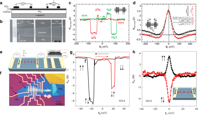
经 Tombros 等人许可转载,Nature 448, 571 (2007) )。版权所有 2007 自然出版集团 [74]。 e –h 经 Avser 等人许可转载,Nat。物理13, 888 (2017)。版权所有 2017 自然出版集团 [84]
横向自旋阀中的自旋传输。 一 非局部自旋输运测量几何。电流从电极 3 通过 Al2O3 势垒注入石墨烯,并在触点 4 处提取。b 单层石墨烯作为自旋传输通道,钴作为四个铁磁电极的四端自旋阀的扫描电子显微照片。 c 4.2 K 处的非局部自旋阀信号。说明了两个扫描方向的电极磁性配置。 d 非局部几何中的 Hanle 自旋进动,作为垂直磁场的函数测量 B z 用于并行配置。 e 黑磷自旋阀示意图。插图显示了异质结构的示意图。 f 设备的光学图像。 g 作为面内磁场函数的非局部自旋阀信号。垂直箭头表示注入器和检测器电极的相对磁化强度,水平箭头表示磁场的扫描方向。 h 非局部几何中的 Hanle 自旋进动,作为垂直磁场的函数测量 B z 用于平行和反平行配置。插图显示了外加磁场下的自旋进动。 一 –d
许多改进的方法用于增加自旋扩散长度和自旋寿命,并且一些器件已经表现出微米范围内的长自旋扩散长度 [13, 77, 78]。例如,在 SiC 上外延生长的石墨烯具有高迁移率,自旋输运效率高达 75%,自旋扩散长度超过 100 µm [79]。 h-BN/石墨烯/h-BN异质结构表现出长距离自旋输运性能,室温下自旋扩散长度可达30.5 μm[13]。二维材料中的自旋输运会受到扩散/漂移的影响,而扩散/漂移可以通过施加电场进行调制。 Ingla-Aynés 等人。 [80] 报道了通过使用载流子漂移在 h-BN 封装的双层石墨烯中达到 90 μm 的自旋弛豫长度。然而,本征石墨烯中较弱的 SOC 和零带隙限制了其在半导体自旋器件中的应用前景。黑磷具有相当大的直接带隙和 1000 cm 2 的室温迁移率 V −1 s −1 ,这使其成为理想的半导体自旋电子材料 [81,82,83]。阿夫萨尔等人。 [84] 构建了一个基于超薄黑磷片的横向自旋阀,并在室温下通过非局部几何测量其自旋输运特性(图 5e,f)。图 5g 中的电子自旋输运表明,随着铁磁体磁化方向的变化,非局域电阻发生变化 ΔR ≈ 15Ω。除此之外,Hanle 自旋进动显示自旋弛豫时间高达 4 ns,自旋弛豫长度超过 6 µm(图 5h)。黑磷中的自旋输运与电荷载流子浓度密切相关,因此可以通过施加电场来控制自旋信号。
旋转操纵
实现对自旋的操纵是有效器件功能化的关键。施加栅极电压可以控制材料中的载流子浓度,这可用于操纵自旋信号 [85, 86]。已经研究了各种作为自旋输运通道的二维材料,以通过施加栅极电压来实现自旋输运参数的调整。例如,偏置诱导石墨烯可以在铁磁体/双层 h-BN/石墨烯/h-BN 异质结构中获得高达 100% 的自旋注入和检测极化 [64]。基于黑磷的栅极可调自旋阀可以达到纳秒范围内的自旋弛豫时间和长自旋弛豫长度[84]。对于半导体 MoS2 通道,施加栅极电压仍然可以获得相对较长的自旋扩散长度,大于 200 nm [70]。然而,合适的自旋场效应器件需要明确的开关比,这对石墨烯乃至半导体二维材料来说都是一个挑战[87, 88]。
为了解决这个问题,已经开发出基于原子级薄石墨烯和半导体 MoS2 的 vdW 异质结构,以通过施加栅极电压实现自旋场效应开关(图 6a)[89]。在这种结构中,结合了石墨烯优异的自旋输运特性和 MoS2 的强 SOC。 The applied gate voltage can change the conductivity of MoS2 and spin absorption during the spin transport, which results in switching of the spin current between ON and OFF states in the graphene channel (Fig. 6b). Another research effort produced a similar report about the graphene/MoS2 vdW heterostructure. In this report, an electric gate control of the spin current and spin lifetime in the graphene/MoS2 heterostructure was achieved at room temperature [90]. Moreover, that report pointed out that the mechanism of gate tunable spin parameters stemmed from gate tuning of the Schottky barrier at the MoS2/graphene interface and MoS2 channel conductivity.

source contact. b Effective B SO as a function of V G。 The inset shows the surface carrier distribution in the Cr-TI layer under V g = − 10 V, + 3 V, and + 10 V. a –c Reproduced with permission from Yan et al., Nat. Commun. 7, 1 (2016). Copyright 2016 Nature Publishing Group [89]. d , e Reproduced with permission from Fan et al., Nat. Mater. 13, 699 (2014). Copyright 2014 Nature Publishing Group [95]. f , g Reproduced with permission from Fan et al., Nat. Nanotechnol. 11, 352 (2016). Copyright 2016 Nature Publishing Group [96]
Spin manipulation. 一 Schematic illustration of a 2D spin field-effect switch based on a vdW heterostructure of graphene/MoS2 with a typical nonlocal magnetoresistance measurement. b The nonlocal resistance R nl switches between R P and R AP for parallel and antiparallel magnetization orientations of the Co electrodes. The spin signal is calculated as ΔR nl = R P − R 美联社。 c The plot with blue circles shows the gate modulation of the spin signal ΔR nl. The solid black line represents the sheet conductivity of the MoS2 as a function of V G。 The insets show the spin current path in the OFF and ON states of MoS2. d Schematic illustration of SOT-induced magnetization switching in a Cr-doped TI bilayer heterostructure. The inset shows illustrations of the Hall bar device and the measurement setting. e Experimental results of SOT-induced magnetization switching by an in-plane direct current at 1.9 K while applying a constant in-plane external magnetic field B y during the measurement. The inset shows an enlarged version of the circled part in the figure. f 3D schematic of the Hall bar structure of the Al2O3/Cr-TI/GaAs stack with a top Au gate electrode. A gate voltage of V g can be applied between the top gate and the
Current-induced SOT is regarded as another efficient strategy to manipulate spin. The spin current, generated by the spin Hall effect within the heavy metals or the Rashba effect at the interfaces, can exert a spin torque to ferromagnets and thereby realize magnetization switching [91,92,93]. Efficient current-induced magnetization switching via SOT may lead to innovative spintronic applications. Due to strong SOC and time-inversion symmetry breaking, magnetically doped TIs are being considered as a promising material to manipulate spin signals via SOT [94]. Wang’s group first experimentally demonstrated a magnetization switching induced by an in-plane current in an epitaxial Cr-doped TI (Bi0.5Sb0.5)2Te3/(Cr0.08Bi0.54Sb0.38)2Te3 bilayer film (Fig. 6c) [95]. The spin Hall angle in the Cr-doped TI film, ranging from 140 to 425, is almost three orders of magnitude larger than that in heavy metal/ferromagnetic heterostructures, and the critical switching current density is below 8.9 × 10⁴ A cm −2 at 1.9 K (Fig. 6d). Furthermore, this team also reported an effective electric field control of SOT in a Cr-doped (Bi0.5Sb0.42)2Te3 thin film epitaxially grown on GaAs substrate (Fig. 6e) [96]. The gate effect on the magnetization switching was investigated by scanning gate voltage under a constant current and an applied in-plane magnetic field in the film (Fig. 6f). The SOT intensity depends strongly on the spin-polarized surface current in the thin film, and it can be modulated within a suitable gate voltage range. The effective electric field control of SOT in the TI-based magnetic structures has potential applications in magnetic memory and logic devices.
In addition, electrical control of emerged 2D magnets has also been investigated. For example, utilizing electric fields or electrostatic doping can achieve the magnetic conversion of bilayer CrI3 antiferromagnetic to ferromagnetic [97]. The coercivity and saturation field of few-layer Cr2Ge2Te6 can be modulated via ionic liquid gating [98]. In contrast to magnetic semiconductor, electrostatic doping can be used to control the carrier concentrations of the ferromagnetic metal, and the ferromagnetic transition temperature of Fe3GeTe2 can be dramatically raised to room temperature via an ionic gate [99]. The emergence and research of 2D magnets provide a new platform for engineering next-generation 2D spintronic devices.
Applications of 2D Spintronics
2D materials exhibit great potential for the engineering of next-generation 2D spintronic devices. Graphene with high electron/hole mobility, long spin lifetimes, and long diffusion lengths is a promising candidate for a spin channel. Moreover, graphene can gain magnetism by introducing adatoms, or magnetic proximity effect [23, 25]. The carrier density in proximity-induced ferromagnetic graphene can be modulated by gating, allowing to observe Fermi energy dependence of the anomalous Hall effect conductivity. This result can help understand the physical origin of anomalous Hall effect in 2D Dirac fermion systems. Realizing a ferromagnetic surface state in a TI is predicted to allow several prominent phenomena to emerge, such as the interfacial magnetoelectric effect [33], and the electric field-induced image magnetic monopole [34]. However, the current technology of inducing magnetism in TI is confined to low temperatures, which restrict its potential for applications. A key requirement for useful applications is the generation of room temperature ferromagnetism in the TI. The PNR result shows that the Bi2Se3/EuS bilayer has a ferromagnetic order at the interface, and this topologically enhanced interfacial ferromagnetism can persist up to room temperature [32]. The topological magnetoelectric response in such an engineered TI could allow efficient manipulation of the magnetization dynamics by an electric field, providing an energy-efficient topological control mechanism for future spin-based technologies.
The STT, and tunnel magnetoresistance (TMR) effects offer alternative approaches for write and read-out operations. The STT effect refers to the reorientation of the magnetization of ferromagnetic materials via the transfer of spin angular momenta. Efficient current-induced magnetization switching via SOT may lead to innovative spintronic applications [71, 100]. Due to strong SOC and time-inversion symmetry breaking, magnetically doped TIs are being considered as a promising material to manipulate spin signals via SOT [93]. TMR refers to magnetization-dependent magnetoresistance behavior. A high TMR ratio is the key to achieve spintronic devices with higher sensitivity, lower energy consumption. 2D materials with high-quality crystal and sharp interfaces can achieve some new functionalities such as spin filtering. The 2D vdW MTJ consists of a 2D magnetic CrI3 layer as a spin filtering tunnel barrier, which reaches a value of TMR up 19,000% [101]. Progress in the fabrication of graphene-based and other 2D heterostructures has led to the optimization of long-distance spin diffusion (up to tens of micrometres), as well as directional guiding of the spin current [13, 64]. Spin manipulation, electrical gating [56], electrical field induced drift [80], SOT-induced switching [95, 96], and the magnetic proximity effect [25, 32] have been explored to develop next-generation MRAM.
2D Spintronic Devices for Memory Storage and Logic Applications
Great efforts have been made to search for new 2D spintronic devices. According to the function, 2D spintronic devices can be classified as memory storage or logic devices. Here we focus on several important 2D spintronic devices, including the 2D magnetic tunnel junction (MTJ), 2D spin field-effect transistor (sFET), and 2D spin logic gate.
2D MTJ
The discovery of the GMR opens the door for 2D spintronics. However, TMR has a stronger magnetoresistance ratio than GMR, so TMR holds greater potential in magnetic storage applications. The TMR structure consists of two ferromagnetic layers and an intermediate insulating layer, which is called the MTJ. The tunneling probability is related to the density of states near the Fermi energy in the ferromagnetic layers. When the two magnetic layers are parallel, the similar density of states for each spin-state can provide more available states for tunneling, resulting in a low resistance state. On the other hand, when the layers are antiparallel, a mismatch between spin channels of the source and sink will result in a high resistance state. Some issues in traditional thin-film MTJs limit the achievement of a high TMR ratio, such as the quality of the insulation barrier and the thermal stability [102]. 2D materials with high-quality crystal and sharp interfaces may offer promising routes to address these issues and even achieve some new functionalities such as spin filtering.
Karpan et al. first explored graphene layers as the barrier in vertical MTJ by computational means in 2007 [103]. They proposed a match between the band structure of graphene and that of nickel, predicting a large spin polarization close to 100%, which can result in a large TMR up to 500%. However, the subsequent experimental results show that the MTJs based on graphene exhibit a very low TMR. Compared to monolayer or bilayer graphene, the few-layer MTJ holds the highest recorded TMR signal of up to 31% in graphene-based MTJs [11, 15]. In addition to graphene, some other 2D materials have been explored as tunneling barrier layers, including insulating h-BN and semiconducting TMDCs [104, 105]. Piquemal-Banci et al. [63] fabricated Fe/h-BN/Co junctions where the h-BN monolayer was directly grown on Fe by using the chemical vapor deposition (CVD) method, observing large spin signals of TMR and the spin polarization of P ~ 17%. MTJs based on MoS2 or WSe2 were reported to have only a few percent of the TMR signal; further exploration is needed to achieve a high TMR ratio.
Emerging 2D magnetic materials exhibit many surprising properties. When the magnetizations in bilayer CrI3 are switched to different magnetic configurations (Fig. 7a), the MTJ based on CrI3 exhibits a giant TMR produced by the spin-filtering effect [101, 106, 107]. As demonstrated in Fig. 7b, the 2D vdW MTJ consists of a 2D magnetic CrI3 layer as a spin filtering tunnel barrier, graphene as a contact electrode, and h-BN as an encapsulation layer to prevent device degradation. The transport result shows that the TMR is enhanced as the CrI3 layer thickness increases, and it reaches a value of 19,000% in four-layer CrI3 based MTJ at low temperature (Fig. 7c) [101]. Subsequently, Xu’s group also reported gate-tunable TMR in a dual-gated MTJ structure based on four-layer CrI3. The TMR can be modulated from 17,000 to 57,000% by varying the gate voltages in a fixed magnetic field [108, 109]. Moreover, with few-layer Fe3GeTe2 serving as ferromagnetic electrodes, the TMR in Fe3GeTe2/h-BN/Fe3GeTe2 heterostructures can reach 160% at low temperature [110]. More interestingly, Zhou et al. reported a theoretical investigation of a VSe2/MoS2/VSe2 heterojunction, where the VSe2 monolayer acts as a room-temperature ferromagnet, and the large TMR can reach 846% at 300 K [111]. On the other hand, the strong spin Hall conductivity of MoS2 holds potential to switch the magnetization of the VSe2 free layer by SOT. Therefore, they put forward the concept of SOT vdW MTJ with faster reading and writing operations, which offers new opportunities for 2D spintronic devices.

Reproduced with permission from Song et al., Science (2018). Copyright 2018 The American Association for the Advancement of Science [101]. c , d Reproduced with permission from Wen et al., Phys. Rev. Appl. 5, 044003 (2016). Copyright 2016 American Chemical Society [118]
2D spintronic Devices. 一 Magnetic states of bilayer CrI3 with different external magnetic fields. b Schematic illustration of a 2D spin-filter MTJ with bilayer CrI3 sandwiched between graphene contact. c Tunneling current of a bilayer CrI3 sf-MTJ at selected magnetic fields. The top inset shows an optical image of the device, and the bottom inset shows the schematic of the magnetic configuration in different magnetic fields. d Diagram of a proposed 2D XOR spin logic gate, where A, B, and M are ferromagnetic electrodes on top of a spin transport channel. 我 s and I out denote the injection and detection currents, respectively. The magnetizations of the electrodes are input logic 1 and 0. The detected current I out serves as the logic output. e 我 out measured as a function of H . Vertical arrows indicate the magnetization states of A and B. The top-left inset shows the table of XOR logic operation. 一 , b
2D sFET
Datta and Das first proposed the idea of the sFET in 1990 [112]. The sFET consists of the source and sink ferromagnetic electrodes, and a two-dimensional electron gas (2DEG) channel which can be controlled by an electrical gate. The gate voltage can result in a spin precession and, consequently, a change in the spin polarization of the current on the channel. Since switching the current through the device requires only little energy and a short time, sFET is expected to be a 2D spintronic device with low power consumption and high computing speed.
As mentioned in the previous section, graphene with high carrier concentration and weak SOC is considered to be a promising candidate as a spin transport channel [113]. Michetti et al. [76] designed a double-gate field-effect transistor structure, where bilayer graphene acts as the transport channel. Theoretical analysis shows that the spin precession of carriers in the graphene channel can be turned on and off by the application of a differential gate voltage. Experimentally, Avsar et al. first reported a dual-gated bilayer graphene structure with h-BN as a dielectric layer, where the spin current propagation in bilayer graphene channel can be controlled by exerting a vertical electric field [114]. The transport results show that the spin-relaxation time decreases monotonically as the carrier concentration increases, and the spin signal exhibits a rapid decrease, eventually becoming undetectable close to the charge neutrality point. A suitable spin field-effect device requires a clear switching ratio, which is a challenge for graphene.
To solve this issue, a graphene/MoS2 heterostructure has been developed to achieve a spin field-effect switch via applying a gate voltage. Two independent groups demonstrated that the applied gate voltage can change the conductivity of MoS2 and result in spin absorption during the spin transport, which gives rise to switching the spin current between ON and OFF states in the graphene channel [89]. Due to the low spin injection efficiency and rapid spin relaxation in channels, it is a challenge to achieve a large high-to-low conductance ratio in 2D sFET device. However, the discovery of 2D magnetic crystals provides new opportunities to explore new 2D spintronic devices. Kin Fai Mak’s group reported a spin tunnel field-effect transistor (sTFET) based on a dual-gated graphene/CrI3/graphene heterostructure [115]. By using bilayer CrI3 as a magnetic tunnel barrier, the applied gate voltage can switch magnetization configurations of bilayer CrI3 from interlayer antiferromagnetic to ferromagnetic states under a constant magnetic field near the spin-flip transition. Distinct from conventional spin transistors, these devices rely on electrically controlling the magnetization configuration switching rather than the signal of spin current in the channel. This technique allows the sTFET devices to achieve a large high–low conductance ratio approaching 400%, which provides a new approach for exploring memory applications.
2D Spin Logic Gate
Dery and Sham first reported a spin logic device based on an “exclusive or” (XOR) gate [116]. The XOR logic gate structure includes a semiconductor channel and three ferromagnetic terminals. An XOR logic operation can be implemented by different spin accumulations, which is caused by different magnetization configurations of the input terminals [117]. Experimentally, the proposed three-terminal XOR logic gate achieved logical operations in a graphene spintronic device at room temperature [117,118,119]. As shown in Fig. 7c, the device includes single-layer graphene as the channel, and three ferromagnetic terminals composed of A, B, and M Co electrodes with MgO tunnel barriers. The magnetization of the electrodes A and B represents the input states 0 or 1, and the current of the electrode M acts as the output state. The magnetizations of input electrodes A and B will be switched by varying an applied external magnetic field, which results in a different spin accumulation in the M electrode, corresponding to a different output current. If the input A and B electrodes have identical contributions to the output M electrode, then the current in the output ferromagnetic terminal has a detectable value only when the magnetization of input ferromagnetic terminals are antiparallel (01 or 10). When the magnetizations of the input ferromagnetic terminals are parallel (00 or 11), the output current is almost zero. Therefore, the XOR logic operation can be achieved (Fig. 7d).
Dery et al. further designed a reconfigurable magnetologic gate with five-terminal structure combining two XOR gates-XOR (A, X) and XOR (B, Y) with a shared output terminal, M [119]. Similar to the three-terminal XOR logic gate, the different magnetic configurations of input electrodes give rise to the different spin accumulation in the output terminal M, which results in different output signals. By analogy, a finite number of these XOR gates can be used to implement any binary logic function. Subsequently, other groups extended this theoretical design to experimental studies by constructing graphene spin logic gates [120,121,122]. Various modeling, simulation, and experimental explorations of 2D spin logic gates have helped to accelerate the progress toward building practical spin logic applications. However, two key issues remain in the research of graphene spin logic gates. The first one is to balance the contributions of two input terminals to the output one. The other one is to eliminate the influence of background signals on the output.
Challenges and Opportunities in 2D Spintronics
As discussed above, much theoretical and experimental research has been carried out to explore spintronics based on 2D materials, and considerable progress has been achieved [15, 123, 124]. However, great challenges still need to be addressed for the practical application of 2D memory and logic applications. We now discuss three of these:physical mechanisms, materials science, and device engineering.
Physical Mechanisms
Due to the complexity of the experiments, the proposed theoretical research and experimental results usually have large discrepancies. For example, based on the mechanism of spin relaxation, theory predicted that the spin lifetime for pristine graphene would be up to 1 μs, whereas experimental values range from tens of picoseconds to a few nanoseconds [14, 57, 103]. Furthermore, the spin injection efficiency of graphene measured experimentally ranges from a few percent to 10%, which is far smaller than the theoretical prediction value of 60–80% [125]. These differences indicate that more in-depth physical mechanisms and accurate theoretical models need to be proposed and developed to better guide the research direction and analyze the experimental results.
Materials Science
2D materials provide an ideal platform to construct various heterostructures for spintronic applications. However, there are still many major problems in 2D materials. For example, stability is a great challenge for 2D materials. Most 2D materials of thickness close to the atomic level are susceptible to moisture, oxygenation, and temperature, especially the recently emerging 2D magnetic materials, which must be peeled off in a glove box with ultra-low water and oxygen content. Besides this, most currently available 2D magnets rely on mechanical exfoliation, and their low magnetic transition temperature is far below room temperature. These are significant limitations because stability in air, convenient wafer-scale synthesis, and operation above room temperature are prerequisites for 2D materials used in practical applications.
Device Engineering
Breakthroughs have been made in the fundamental study of 2D spintronics, such as enhanced spin injection efficiency by using 2D tunnel barriers h-BN, long spin diffusion length up to 30 μm at room temperature in graphene-based 2D heterostructures [13], and high TMR up to 19,000% by using 2D magnets as spin filter barriers [101]. Based on the study of 2D spintronic devices, it is promising to develop the low-power device applications, including advanced magnetic memories and spin logic circuits, which are compatible with the existing complementary metal-oxide semiconductor (CMOS) electronics. However, the design and application of functional 2D spintronic devices are still in the early theoretical prediction and proof-of-concept stage.
Opportunities
2D spintronics is an important scientific research field with many potential applications for future technologies. As mentioned above, considerable challenges currently remain, but there are also many opportunities. Spin valves based on graphene as the spin transport channel can exhibit a long spin diffusion length up to 30 mm at room temperature [13]. Magnetic tunnel junctions with four-layer CrI3 as spin filter tunneling barriers show giant TMR up to 19,000% at low temperatures [101]. The magnetic transition temperature of Fe3GeTe2 can reach above room temperature via an ionic liquid gate or when tailored by a TI [99, 126]. Spin-polarized current can be injected from WTe2 into magnetic substrates by SOT switching [127]. New concepts of spin tunneling field-effect transistors based on 2D magnets CrI3 have been proposed as well. The demonstration of giant TMR, the efficient voltage control of 2D magnetism, and the magnetization switching in 2D magnets by STT or SOT all open up opportunities for potential next-generation spintronic devices based on atomically thin vdW crystals [21, 100].
结论
The study about the magnetic properties of 2D materials is of great significance to the development of 2D spintronics. The magnetic interaction in graphene and TIs has scarcely been explored, and recently discovered 2D magnets also provide an ideal platform to study 2D magnetism. Great progress has been made in 2D spintronics in recent decades, especially in graphene spintronics. However, the origin of spin relaxation in graphene is still a major open question, and further improvement in the spin lifetime and spin diffusion length remains an important research direction for graphene-based spintronic devices. The practical application of 2D spintronic devices still requires meeting great challenges, including related physical mechanisms, materials science, and device engineering. The development of technology, the improvement of theoretical models, and the exploration of new materials all provide more opportunities for new-generation 2D spintronic device applications in the future.
数据和材料的可用性
不适用。
缩写
- 二维:
-
二维
- GMR:
-
Giant magnetoresistance effect
- STT-MRAM:
-
Spin-transfer-torque magnetoresistive random-access memory
- vdW:
-
范德华
- SOC:
-
Spin–orbit coupling
- TMDCs:
-
过渡金属二硫属化物
- TIs:
-
Topological insulators
- 鱿鱼:
-
超导量子干涉装置
- YIG:
-
Yttrium iron garnet
- QAHE:
-
Quantum anomalous Hall effect
- PNR:
-
Spin-polarized neutron reflectivity
- MOKE:
-
Magneto-optical Kerr effect
- MBE:
-
分子束外延
- h-BN:
-
六方氮化硼
- SOT:
-
Spin–orbit torque
- ST-FMR:
-
Spin-torque ferromagnetic resonance
- MTJ:
-
Magnetic tunnel junction
- sFET:
-
Spin field-effect transistor
- TMR:
-
Tunneling magnetoresistance
- CVD:
-
化学气相沉积
- 2DEG:
-
Two-dimensional electron gas
- sTFET:
-
Spin tunnel field-effect transistor
- XOR:
-
Exclusive or
- CMOS:
-
Complementary metal-oxide semiconductor
纳米材料