

使用第一性原理方法的电掺杂纳米级器件:综合调查
摘要
掺杂是半导体器件制造的关键特征。在过去的几十年中,已经发现了许多用于控制半导体物理领域掺杂的策略。电掺杂是一种很有前途的策略,可用于有效调整电荷数量、电子特性和传输特性。这种掺杂过程降低了高温和异物污染的风险。在过去的几十年里,大量的实验和理论努力被证明用于研究电掺杂的特性。在本文中,我们首先简要回顾了电掺杂的历史路线图。其次,我们将在分子水平上讨论电掺杂。因此,我们将回顾一些分子水平的实验工作,同时回顾基于电掺杂进行的各种研究工作。然后我们找出电掺杂的重要性及其重要性。此外,我们描述了电掺杂的方法。最后,我们对电掺杂方法与常规掺杂方法进行了简要的比较研究。
介绍
掺杂在决定各种有机或无机材料的物理特性及其应用方面起着至关重要的作用,尤其是对于半导体。该方法已在半导体物理行业得到成功验证。少量杂质的加入决定了材料的掺杂浓度和电导率。据观察,理想的掺杂剂应在其主体材料中表现出理想的溶解度,并且还表现出低缺陷水平。然而,这种传统的掺杂工艺存在一些基本问题,例如严重影响器件性能的掺杂瓶颈。在宽带隙材料中已经观察到这种类型的性能下降。
例如,在高导带器件的最小值的情况下,n 型掺杂具有挑战性,而对于低价带器件的最大值也很复杂 [1, 2]。因此,宽带半导体中的双极掺杂工艺出现了一些问题。据观察,可以插入 p 型或 n 型掺杂剂,但不能一起插入 [3]。因此,为了弥补此类问题,已将可行的解决方案纳入掺杂领域。这种类型的提议方法称为电掺杂,它不依赖于这种类型的双极掺杂。已引入电掺杂以解决双极掺杂的问题。在 80 年代后期和 1990 年代,研究人员观察到像 GaN 单晶这样的 III-V 族化合物难以生长。更重要的是,在 1990 年代后期,GaN 衬底也无法用于商业用途。其背后的原因解释为蓝宝石衬底和GaN半导体的晶格常数和热膨胀系数之间的差异使得难以在蓝宝石衬底上生长高质量的GaN基外延层。另一方面,由于高 n 型背景浓度和低 p 型掺杂活性的组合,几乎不可能获得 p 型 GaN 半导体。使用 Rudaz 在 1998 年的电掺杂现象可以显着克服这个问题。在 1980 年代后期,科学家们发现了生长 GaN 或 AlN 缓冲层以在低温下演示基于 GaN 的 LED 的重要性。生长后热退火工艺有助于激活 GaN 缓冲层中 p 型掺杂剂的生长。这些进步加速了用于宽带光电器件的 III-V 族氮化物半导体材料系统的器件开发[4]。 GaN 衬底和生长后热退火工艺也在该技术中发挥重要作用 [5,6,7]。近几十年来,等离子蚀刻技术在超大规模技术 (ULSI) 中发挥着重要作用,可缩小图案尺寸。这使我们看到了纳米技术的发展。与此同时,等离子技术面临一些固有的问题,例如;电荷积累、光子紫外线辐射以及纳米器件的蚀刻性能。为了解决这些问题并制造实用的纳米级器件,中性束蚀刻工艺已进入该领域。 S. Samukawa 介绍了这种中性光束源,还谈到了前景纳米器件的自上而下和自下而上处理的组合。中性光束技术是无损伤蚀刻,因为它是原子使用的。也可以使用这种技术对无机和有机材料进行表面改性。该技术是未来纳米器件实用制造技术的有力竞争者 [8]。这种高密度等离子体技术包括电感耦合等离子体 (ICP) 和电子回旋共振 (ECR) 等离子体,它们是实施这种等离子体技术的关键方法。但是这种技术有几个问题,例如
-
各种类型的辐射可能会破坏正离子和电子的电荷积累[8,9,10,11,12]。
-
紫外(UV)、真空紫外(VUV)射线的辐射也可能对纳米级器件造成损伤。
-
在此等离子体蚀刻问题中,X 射线光子也可能导致纳米级器件破裂 [13,14,15,16,17,18,19,20,21]。
-
由于电压产生导致的电荷积累扭曲了离子轨迹,也会导致薄栅氧化膜破裂。
-
除此之外,高密度等离子体刻蚀技术辐射的UV或VUV光子会导致产生晶体缺陷。
这些问题极大地降低了纳米级器件的电性能。因此,使用高性能中性束蚀刻系统可以避免这些问题。 S. Samukawa 和他的团队发明了一种高效的中性光束源,以实现未来纳米级器件的终极自上而下蚀刻。他们使用我们新的中性光束源为未来从 50 纳米到 10 纳米以下的纳米级器件引入了终极蚀刻工艺。
因此,这封信的组织如下。首先,简要回顾了电掺杂的历史路线图。之后,我们将回顾一些分子水平的实验工作,因为这种掺杂过程对分子水平也有影响。然后,我们简要讨论了与电掺杂过程相关的各种研究工作。以下部分描述了电掺杂的一些重要性。此外,我们描述了电掺杂过程的方法。最后,我们将简要讨论常规掺杂与电掺杂的对比研究。
电子兴奋剂的历史路线图
尽管这项研究主要集中在分子水平上的电掺杂,但重要的是首先回顾一下常规掺杂的早期历史。 1930年,人们注意到由于存在少量杂质而影响半导体的导电性[2, 22, 23]。 1931 年,第一个量子力学形式被用于半导体材料 [24]。 1938 年,Davydov 成功演示了 p-n 结的原型 [25, 26]。本文解释了少数载流子的重要性。伍德亚德引入了“兴奋剂”的概念。他将一小部分磷、砷或锑掺入纯锗中。这种杂质的添加增加了锗的电性能 [27]。肖克利在 1949 年提出了他的历史发明,即“结型晶体管”。这项发明改变了半导体工业的几何结构 [28]。虽然双极结的发明给半导体行业的发展带来了海啸,但它也存在一些与晶体管相关的问题。例如,两个 p-n 层应该在一个薄的空间内背靠背连接在一起。这个问题在 1950 年贝尔实验室使用双掺杂方法发明“生长结晶体管”后被解决 [29, 30]。在“双掺杂”工艺的情况下,在熔融的 n 型锗中加入一撮镓,将锗转化为 p 型。之后,其中包含少量锑,将其从 p 型转变为 n 型 [31]。在此过程中,两种类型的掺杂剂被背靠背添加。另一种兴奋剂是在 50 年代初期发展起来的,称为“共同兴奋剂”。 p 和 n 结被认为是半导体的“共掺杂”。分子水平的掺杂也是电掺杂的重要组成部分。 1998 年,Rudaz 提出了一种通过减少 III-V 族半导体材料开裂来最大化电掺杂效果的方法[4]。 2002 年,Zhou 等人。展示了真空沉积透明有机发光二极管,它也是一种使用电掺杂工艺的低电压器件。电掺杂对于提高有机器件的性能起着至关重要的作用。电掺杂载流子注入发生在有机 LED (OLED) 中。传输层显示低驱动电压,这通常是由于电极界面末端的自由基阴离子、阳离子和欧姆接触。超低电压 OLED 以 2.6 V 真空沉积,100 cd/m 2 在 p-i-n 结构中。因此,本征发射夹在 p 型和 n 型宽带隙传输层之间。一些研究强调了与有机分子膜中电掺杂有关的活动[32,33,34,35,36,37,38,39,40,41,42]。
这是在原子级器件设计方法中避免离子轰击过程的程序之一。 Gao 和 Kahn [43] 已经在分子薄膜上证明了这个过程。这些化合物例如具有三(4-溴苯基)六氯锑酸铵(TBAHA) 4,4',4″-三(3-甲基苯基苯基氨基)-三苯胺(m-MTDATA)空穴传输层p掺杂F4-TCNQ的聚碳酸酯聚合物用于成功制造各种 OLED 复合器件层 [45, 46]。该工艺也已用于有机光伏电池 (OPVC)。该过程还被用于分子水平的调谐,以及通过载流子注入提高器件效率。通过使用该工艺,对于 n 型和 p 型掺杂,分子膜电导率在很大程度上增加。这种掺杂工艺广泛用于无机半导体上的欧姆接触 [43,44,45,46]。如今,有机 LED 在分子纳米技术领域占有重要地位。在 III-V 族半导体中,使用这种掺杂工艺可以使 n 型接触和 n 型外部分子的插入成为可能。电掺杂还有助于使诸如电阻、载流子插入、载流子复合到分子界面层中的现象成为可能。有机光伏电池 (OPVC) 是电掺杂现象最相关的应用之一。在 OPVC 的电平对齐过程中,该过程作用于这些电池的电导率。这种方法最终会增加电荷载流子的插入。在元有机界面的情况下,该方法开始并引入耗尽层的布置,通过该耗尽层可以发生量子隧道传输。这是可有效用于有机和无机接触制造的有效工艺之一。该过程还有助于改变分子薄膜的电荷中性水平。除此之外,使用这种方法可以将大约 0.1% 到 1% 的外来分子包含在分子界面上。这个掺杂浓度对于传统的掺杂方法来说是一个很大的数字。这种掺杂浓度水平有助于产生退化的半导体。这种高掺杂浓度有助于防止随后形成诱导带 [34, 43,44,45,46]。
电子兴奋剂过程及其重要性
选择电掺杂方法的主要和最重要的技术是使用该过程控制费米能级。因此,该技术在过去几十年中在无机和有机半导体中非常流行。近年来,电掺杂在仿生纳米技术领域引起了特别关注。电掺杂是将电荷插入或接受到分子膜的过程。该工艺的关键特征是不能限制传统的 n 和 p 掺杂来实现双极性。传统的电离工艺不适用于这种类型的电掺杂工艺 [43,44,45,46]。引入了电掺杂程序以避免离子轰击,这在纳米级器件建模中通常是不可能的。
这种掺杂方法主要分两步确定:
-
第一步涉及从供体到受体(转化为分子)的单电子转移。
-
其次,它与基态整数电荷转移络合物的解离方法有关。
因此,证实电掺杂只不过是将费米能级向最高占据(价带)分子能级或最低未占据(导带)分子态移动。如果自由载波是ρ , N A − 是离子化掺杂剂密度,N A 是中性掺杂剂浓度,那么自由载流子密度将被公式化为公式。 (1).在这个等式中,E A 和 E F 是受主和费米能级能量和 K B 是绝对温度下的玻尔兹曼常数 T [124].
$$\rho =N_{{\text{A}}}^{ - } =\frac{{N_{{\text{A}}} }}{{1 + \exp \left( {\frac{{ E_{{\text{A}}} - E_{{\text{F}}} }}{{K_{{\text{B}}} T}}} \right)}}$$ (1)这种掺杂技术是在 Atomistix Tool Kit-Virtual Nano Lab (ATK-VNL) 中使用双探针设计技术实现的。仿生原子装置的数量是纳米技术的核心。这些设备在超高太赫兹频率下运行。为这些设备计算的频率约为 THz。例如,在一篇文章中,说明了 GaAs-腺嘌呤-GaAs 半导体隧道结的传输特性。在那篇文章中报道的工作频率约为 25THz [125]。
掺杂是为了增强电性能而有意将外部杂质引入纯半导体材料中。电掺杂工艺的重要性可描述如下。
这种电掺杂工艺不同于传统的掺杂工艺。在常规掺杂工艺的情况下,半导体材料掺杂有外来掺杂剂或杂质。这个过程就是高温过程。在这种高温掺杂过程中可能会发生键断裂。也采用电离方法来实现这种掺杂方法。另一方面,电掺杂工艺与杂质完全无关。在这个过程中,在设备的两端感应出相反电位的电荷。因此,它将在纳米器件的中心分子区域产生电位降。这种方法对纳米器件设计非常有帮助,因为电离方法可能会产生纳米材料的结构变形。在常规掺杂的情况下,可能会出现几个问题。表 1 列出了一些主要问题。表 1 列出了传统掺杂和电掺杂之间的区别,这也有助于理解电掺杂对纳米级器件制造的重要性。
此表 1 显示了为什么电掺杂对分子水平很重要。这种掺杂避免了发热、原子间或分子间反应,并且兼容任何类型的纳米级器件设计程序。
本文主要重点介绍电掺杂工艺。这种掺杂方法可用于纳米级器件制造,主要是分子薄膜制备。在这种方法中,电荷载流子的插入发生在分子装置的两端。图 1 中也描述了该过程。该图表示简单的电掺杂方法。该图还显示了由于在电极的两个端子处插入两个相等但相反的电荷载流子插入而产生的电位降。这些电极是分子器件的重要组成部分。电荷插入可以通过这些电极完成。这种相等且相反的电荷会在中心分子区域内产生电位降。这种电位降作为两个电极之间电荷传导的驱动力,即通过中心分子部分。这是电掺杂的实际过程。虽然该过程目前主要用于纳米级器件的分析或理论建模,但也可用于有机和无机分子薄膜的制备。
<图片>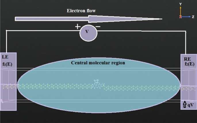
概念电掺杂工艺示意图
图 1 显示了电子或电荷载流子如何从一个电极流向另一个方向,这是由于电极两端的偏压变化造成的电位降。
分子水平的电掺杂
最近研究人员对受控掺杂程序感兴趣。因此,这种电掺杂程序有助于为无机半导体引入受控掺杂。因此,通过引入电掺杂来调整这些半导体的电特性也很有帮助。这种掺杂现象有助于通过半导体的化学变化来调整半导体的光学间隙。这种掺杂工艺也是一种低成本工艺,可用于柔性基板。
电掺杂程序是在纳米器件的两端之间产生电位差的方法。在这项理论工作 [47,48,49,50,51,52] 中,我们通过两个探针电极在纳米器件的两端提供不同极性但相同值的电压来安排这一点。该理论过程的示意图如图 2 所示。
<图片>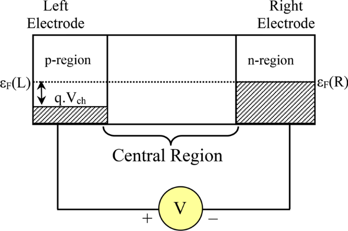
概念电掺杂工艺示意图(使用ATK-VNL)
这种理论方法涉及创建高度掺杂的正 (p+) 和负 (n+) 区,这对于设计用于有机和无机材料的纳米半导体器件很重要。
使用此程序将电荷载流子注入分子界面。电掺杂是有机分子而非无机薄膜的受控过程。因此,传统的 p 和 n 掺杂剂对于插入不是强制性的。最终,电掺杂会增加载流子注入并降低驱动电压,从而提高器件效率。因此,电掺杂方法完全依赖于向主体分子注入电子传输或电子接收。
异质结链由腺嘌呤和胸腺嘧啶生物分子制成,当异质结链穿过 GaAs 纳米片的纳米孔时,用于感应多种气体[47]。在这种情况下,还会在该纳米片的两个部分感应电掺杂。由于有效的电感,该生物分子链显示出其感知吸附的外来气体分子的能力[47]。在纳米器件设计的情况下,也处理分子的吸附。例如,研究了在 32°C 温度下挥发性分子吸附到 ZnO 纳米线中 [53]。使用基于 DFT 和 NEGF 形式的第一原理方法,可以使用各种结构修改来设计纳米 FET。还观察到这些纳米 FET 的各种特性,例如可扩展性评估、最高占据分子轨道 - 最低未占据分子轨道 (HOMO-LUMO) 间隙、最大可获得电流、RF 性能、线性研究 [54,55,56, 57、58、59、60、61]。可以使用基于 DFT 和 NEGF 的形式来设计基于共轭共寡聚体的分子二极管。共聚低聚物与两个电极相连,形成分子二极管。分析了该二极管的能隙、电流-电压 (I-V) 特性、空间方向 [62]。第一性原理方法应用于使用不同连接体从碳纳米管 (CNT) 衍生出的七个不同结的几何优化纳米结构 [63]。可以使用基于 DFT 和 NEGF 公式的第一原理方法来实现各种类型的二极管。例如,肖特基二极管、单分子二极管、自旋电流二极管、双极自旋二极管、双块分子二极管、反向二极管特性因此使用这种方法实现[64,65,66,67,68]。
基于电掺杂的分子级研究工作
分子水平的电掺杂在纳米电子学中起着重要作用。研究人员非常有兴趣在纳米器件设计过程中引入这种掺杂过程。这种掺杂的效果有助于在不同分子水平的排列之间进行交互。该过程不仅有助于研究有机异质结的分子水平,而且对于无机材料也是可以接受的。这种掺杂有助于在分子界面相对位置的偶极子和等效移动的帮助下形成界面。因此,这种电掺杂过程对于分子界面排列是可以接受的。
传统电子设备的小型化是当今最新兴的研究领域。有几种方法可以激发研究人员调查和研究纳米器件的性质。最重要的方法之一是设计和模拟分析纳米结构。可以使用该模拟程序设计许多重要设备并分析获得的结果 [47, 55, 56]。根据结果,研究人员可以修改各种模拟参数以及纳米级分析模型的不同方面。在这些模拟方法中,第一原理方法是最有效和最流行的过程。电子设备的现代化鼓励研究人员在修改后的版本中对传统设备进行创新。例如,传统的半导体器件可以使用生物分子进行设计。通常在生物分子的情况下,核碱基如腺嘌呤、胸腺嘧啶、鸟嘌呤和胞嘧啶被认为是 DNA 的基本构建块 [47, 55]。在纳米技术领域,构建传统的无机半导体器件非常普遍。然而,主要使用生物分子构建有机电子器件是很困难的。这些半导体的特征取决于掺杂特性。如果半导体没有任何杂质掺杂,则称为本征或纯半导体。另一方面,如果半导体掺杂了外来原子或分子,则它被称为外在或不纯半导体[55,56,57,58,59,60]。
如今,纳米器件设计对研究人员来说是一个具有挑战性的方面。二极管、晶体管、逻辑门已经在分子水平上实现了。研究人员还可以在分子水平上实施纳米生物半导体器件。其中一些生物分子装置已被引入生物医学领域。这些纳米器件的理论设计已使用基于 Atomistix-Tool Kit 和虚拟纳米实验室 (ATK-VNL) 的 Quantumwise 软件模拟器 13.8.0 版实现 [69,70,71,72,73,74,75,76] .甚至量子元胞自动机 (QCA) 逻辑也可以使用基于 DFT 和 NEGF 的第一原理方法在理论上实现[77]。可以使用生物分子设计各种逻辑门,从这些理论含义中获得的结果也已使用 Multi-Sim 或 SPICE 或其他模拟器进行验证 [70]。电掺杂工艺是引入以获得最佳电流的关键特征。通过分子通道的隧道电流受多种因素的影响,如背向散射效应等。通过实施这种掺杂工艺,我们可以避免传统掺杂工艺相关的问题。肖特基势垒调谐的偶极子组合模型也在分子水平的金属-半导体界面上提出 [78]。第一性原理方法也适用于磁隧道结,并且已经分析了它们的量子电子特性[79]。为了计算通过基于 SiO2 和 SiOxNy 的 MOSFET 的漏电流,研究人员使用了基于 DFT 和 NEGF 的第一原理方法 [80]。这种 ab-initio 建模适用于使用钇和硅化镍原子级界面的肖特基势垒高度调谐建模 [81]。可以使用 DFT 和 NEGF [82] 描述反向偏置 MOS2 p-n 结纳米带中的直接带间隧穿。将相反极性的掺杂原子掺入纳米线的效果表现出像齐纳二极管一样的电气特性 [83]。在半金属亚硝酸钇 YN2 [84] 中可以看到双自旋过滤效果。可以使用这种电掺杂技术观察异质结构生物分子 FET 的研究。可以在分子水平上使用这种电掺杂现象观察量子弹道传输 [85]。当使用单壁碳纳米管 (SWCNT) 作为电极时,使用这种理论方法设计了电掺杂生物分子开关 [86]。 NEGF 形式有助于设计基于石墨烯的反点谐振隧道二极管 [87]。二维硅 p-n 结的原子特性已使用第一原理方法证明 [88]。二极管和晶体管是任何电子电路的基本构建块。逻辑门也可以使用二极管和晶体管来实现。因此,任何逻辑都可以使用第一原理形式来实现。
在纳米技术的最新趋势中,研究人员有兴趣在原子尺度上设计和表征仿生和半导体器件的各种机电特性。这些仿生设备具有高度的生物相容性,并在半导体领域和双分子研究领域之间架起了一座桥梁。 CMOS技术已经饱和。因此,研究人员的目标是在它们之间进行替换和搭建桥梁。研究人员已经提出了几项建议,将 CMOS 技术与 DNA 或任何其他生物分子等仿生技术结合起来。 DNA 的重要部分是腺嘌呤、胸腺嘧啶、胞嘧啶和鸟嘌呤氮碱基。这些氮碱基与核糖和磷酸基团复合形成寡核苷酸。该寡核苷酸以磷酸基团为骨架。动态信号的相关性已增强,可用于识别生物分子和 DNA [89]。通过石墨烯纳米孔的 DNA 易位、电子传输和半经验建模也可以在理论上使用 DFT 和 NEGF [90,91,92,93]。使用半经验建模的石墨烯电极也可以进行 DNA 分析 [94]。使用横向运输特性识别核酸碱基对也已成为可能[95]。研究小组还提出了通过射击 DNA 的电导 [96]。通过掺杂程序对 DNA 碱基对进行电子增强也已被纳入以提高电导率 [97]。双质子转移过程也使电子促进成为可能[98]。使用第一原理方法也可以通过交叉隧道方法识别核苷酸 [99]。结构因素控制着 DNA 的电导率,这也在 [100] 中进行了讨论。对于不同类型的纳米器件建模,纳米器件表现出巨大的量子传输现象 [56, 58, 59, 101,102,103,104,105,106,107]。这些器件包括 FET、二极管和光开关 [60, 68, 108,109,110,111,112,113,114,115,116]。这项提议的工作是利用 III-V 半导体技术在生物分子之间架起桥梁的一种方法。生物分子和 III-V 族纳米晶材料的异质结构也可以使用第一性原理理论方法进行设计。此外,使用第一性原理形式研究了氮和金共掺杂石墨烯的电学和光学性质。第一性原理形式主义用于发现量子力学特性的变化以及研究有机和无机分子的各种电子或光学性质。也可以研究空位缺陷石墨烯和掺杂锰的石墨烯对 H2S 的吸收。使用第一原理方法对过渡金属掺杂的 AlN 单层进行铁磁性研究也是一个新兴趋势。对可见光使用 DFT 研究单层 MoS2 的掺杂效应是一个重要的讨论话题。 A study of change of electronic properties was demonstrated for Eu-doped phosphorene based on the first-principle approach. Electromechanical quantum transport features are available for these devices [117,118,119,120,121].
In the year of 1987, Destefanis proposed the electrical doping of HgCdTe using ion implantation and heat treatment method. To increase a large number of pixels into the focal plane array devices, infrared photovoltaic detectors were required. The use of ion implanting HgCdTe was increasing this interest of manufacturers. In this type of manufacturing of photovoltaic infrared detectors, the electrical doping process was introduced. It was revealed that the effect of electrical doping into HgCdTe appeared significantly as the intrinsic properties of diodes were directly related to it [122]. Electrical was also proposed for enhancement of plasmonic absorption on Au-PbS core–shell nanocrystals. This method of doping was implemented using the intra-particle charge transfer method. In this experiment, colloidal nanocrystals were used to be the basic building blocks for solar cells, photo-detectors, etc. In this approach, researchers investigated the electronic properties of colloidal nanocrystalline materials and they also proposed a novel approach to electrical doping to these nanocrystalline solids using intra-particle charge transfer method [123]. The process flow for this simulation work is shown in Fig. 3.

Working flowchart diagram of Quantumwise ATK-VNL [76]
Simulation Methods of Electrical Doping
The analytical design of these molecular devices requires constant innovation and improvement in the field of material science. Density functional theory (DFT) and non-equilibrium Green’s function (NEGF) are the two key formalisms behind the analytics for the modeling of these nanoscale devices. The first-principle approach combines these two formalisms to describe theoretically these types of nanodimension devices. Extended Hückel theory (EHT) is another key factor to accelerate the design procedure of these atomistic devices [126, 127]. These theoretical modeling procedures help to prevent various problems regarding the nanoscale design like hazards during doping of foreign particles, generation of THz operating frequency, etc. Another aim of this nanoscale design procedure is to operate the device by keeping the electronic temperature at 300 K, i.e., room temperature. III–V semiconductors are optically sound semiconductor material that can be used for the design of various electronic devices. After silicon technology, III–V semiconductor technology is one of the emerging and most desirable areas to be fit in the nanoscale semiconductor technology. Biomolecules (like adenine, thymine, guanine and cytosine) have been introduced to form different nanoscale electronic devices. These biomolecules also exhibit their optical exposure whenever they are simulated at near-UV region (mid-UV-B). In this proposed work the electronic characterization has been made for the simulated nanoscale devices using the first-principle approach. This semiempirical modeling is carried out using EHT for obtaining faster simulation. We aim to design and characterize the III–V materials along with biomolecules using DFT- and NEGF-based first-principle formalisms. This semiempirical design of this bioinspired nanodevices has been carried out using the Quantumwise software simulation package.
To include electrical doping into the molecular devices, the same but opposite charge is to be provided to the two ends of the molecular interface. The electrical doping concentration is calculated using the following procedure:
Let us assume the electrodes are about 1 nm long and with 0.5 nm × 0.5 nm cross-sectional area. For simplification of calculation, we have taken those values. In the script editor, we have located the section for the electrodes calculator and assigned the charge = + 0.01 and − 0.01. For this theoretical study, the Atomistic Tool Kit-Virtual Nano-laboratory (ATK-VNL) software package has been used. This software uses density functional theory (DFT) and non-equilibrium Green’s function (NEGF)-based first-principle approach. This value is being calculated using the following formula:
-
Effective doping concentration = doping/volume [1, 70, 71]
-
Assume, doping charge = ± x V
-
Assume that, volume = length (a ) × width (b ) × height (c ) = a × b × c
-
Volume = (a × 10 –7 ) × (b × 10 –7 ) × (c × 10 –7 ) cm −3 = abc × 10 –21 /cm 3
-
Effective doping = \(\frac{x}{{abc \times 10^{ - 21} }}\) = abc × 10 21 /cm 3 [as we have consider the dimension in nm unit]
The volumes of the electrodes remain constant so from Fig. 4, it can be observed that the doping concentration is directly proportional to the applied bias voltage. This is another reason that we have kept constant the electrode’s size. The little change in electrodes’ size leads to a large change in electrical doping concentration. So by changing the little amount of bias voltage we can be able to generate very high electrical doping into the system using the first-principle approach.

Dependence of effective electrical doping on an applied bias voltage
The electrical doping in this case totally depends on two parameters mainly. They are (1) effective doping charge (charge applied at the two ends of the electrodes) and (2) volume of the nanoscale device. Therefore, the formula of calculating electrical doping is mentioned as doping/volume, so if the length, height or breadth or anyone of the parameter is changed, then the doping concentration is definitely changed. For this type of device structure, volume is a function of length, height, width [70].
Both the temperature and thickness affect the performance of these nanoscale devices. Self-heating effect along with thermal noise generated heat also makes changes in quantum-ballistic transport phenomenon of these devices at this low dimension. Therefore, temperature plays an important role in the device performance. On the other hand, as thickness is related to the volume of the device and effective doping is directly related to volume, thickness also affects device performance. If thickness is changed, then accordingly volume changes which result in changes of doping concentration. Doping concentration is related directly to device performance like channel conductivity, current–voltage characteristics, etc., for these nanoscale devices. Therefore, doping is changed due to thickness changed that will definitely change device performance [70].
Evolution of Electrical Doping
Doping means the addition of explicit impurity atoms to the semiconductor. Doping is the intentional addition of atoms to the intrinsic semiconductor to modulate the electrical properties of intrinsic semiconductors. The electrodes sizes are inserted within the script editor, where we assigned the length of the electrode as 1 nm and cross section 0.5 nm × 0.5 nm. Thus, the nominal charge, i.e., ± 0.01, is set for the two electrodes. This script is processed through the job manager, and the calculated doping value for the electrodes is obtained. For this calculation we pursue the following steps:
-
Open the New Calculator and select “ATK-SE:Extended Hückel (Device).”
-
Uncheck “No SCF iteration.”
-
Keep mesh cutoff to 10 Hartree.
-
Under “Poisson Solver” set the “Neumann” boundary conditions along A(X) and B(Y) directions.
Figure 5 shows the consolidated form of the comparative study between electrical doping and conventional doping process (using Fe and Ni). This analytical experiment is observed for the thymine nanotube structure which is an example of electrical doping [70]. Fe and Ni atoms are chosen to dope the thymine nanotube, and on the other hand, the molecule is electrically doped [70]. All these results show that amount of electrical doping is much more when compared with conventional doping for little amount of applied bias. Some example works of electrical doping along with its some advantages over conventional doping are discussed in Table 2. It gives a comparative study of electrically doped devices with the existing device modeling which follows the conventional doping method. There are several types of doping, and dopants are available, for example, conventional doping (by adding impurity), electrical doping, co-doping. Generally, two types of dopants are available for conventional doping process, p-type dopants and n-type dopants. They are often called as acceptor and donor impurity atoms. These external impurities are added to the semiconducting materials to enhance their electrical properties mainly conductivity. In the case of the electrical doping process, mainly for analytical modeling using the ATK-VNL approach, we do not proceed with the addition of foreign atoms. Instead of these explicit atom doping, we focus on the change of potential difference at the two ends of the device (mainly at the ends of electrodes). The doping of a semiconductor along with another substance is known as co-doping. For example, when Co and N both are added to MoO2 nanowires, it will increase the electronic performance of this nanowire [128,129,130]. Various properties like electronic, optical and morphological characteristics of p-doped polyfuran (PF) molecular thin films were investigated by the researchers using a wide range of doping ratios using the electrical doping method. When the doping concentration is ≤ 2%, then it increased the short-circuit current of this PF-based photovoltaic device significantly [44].

Comparative diagram at various electrical dopings along with conventional Fe- and Ni-doping
If we take a close look at the doping concentration from Fig. 6, we can observe that before the year 2000, doping concentration was high, but after that, it becomes lower. Therefore, it can be emphasized that though the device performance has been enhanced, doping concentration is reducing very fast [124, 128, 134,135,136].

Doping concentration year-wise graph
The optical and electrical doping process was also introduced into the silicon with holmium in the year 1999. Intermolecular hybridization state is also governed by the electrical doping process. It was established that for organic semiconductors, molecular electrical doping was found to be at odds when other methods were proved in this field, for example, the formation of polaron. Therefore, the main objective of this study is to propose a polaron-derived state with decreased ionization energy using ultraviolet photoelectrospectroscopy [134]. The electrical doping profile in ferroelectric film capacitors was investigated by the group of researchers using capacitance–voltage measurement. In this experimental study, profiling effect of electrical doping concentration in ferroelectrics was investigated using the following effects of
-
A field and spatially dependent permittivity.
-
Domain switching analysis of Schottky profiling [135].
From Fig. 7, we can observe the operating temperature for this type of doping-dependent device operation. Though the graph is a little bit complex, it does not obey any specified rule. Therefore, we can conclude it like that temperature requirement is solely depending on the type of materials that are used for this operation.

Temperature for doping
A new model was proposed for the dissociation of carbon atoms at the copper/silica molecular thin layer interface using catalytically hydrogenated graphene meshes using a semipermanent electrical doping method. This process enables stable electronic doping through C–N bonds. Furthermore, the effect of trap states on the electrical doping for organic semiconductors was also investigated. The direct charge transfer process from the trap state of the host molecules to the dopant molecules raised the electrical effect for organic semiconductors. This type of doping process enhances conductivity. Therefore, trap density and energy are also analyzed using impedance spectroscopy [136].
It is observed clearly from Fig. 8 that the thickness of the wafer layers is reducing year wise. The more the time increasing, the layer thickness reduces, and the performance of the device increases.

The thickness of the wafer
Electrically doped and undoped poly(9,9-dioctylfluorenyl-2,7-diyl) (PFO) along with tetrafluorotetracyanoquinodimethane films were composed using photoelectron spectroscopy method and also investigated their current–voltage characteristics. Thus, it can be observed that the depletion region was created for the PFO interface. Therefore, the current was increased subsequently [137, 138]. For high-temperature gas sensors, this method of doping plays an important role. The conductivity and gas sensitivity of Ga2O3 thin films was investigated. It was observed that this doping concentration influenced the surface sensitivity [138].
From Fig. 9, it is observed that the cutoff wavelength of the devices reduces sharply within a few decades. Hence, device performance enhanced significantly. Table 3 gives a close look at different characteristics of the devices which follow either electrical doping or conventional doping procedure.

The wavelength of the devices reduces
In this survey, we have reviewed the works which were already established using the electrical doping process. In our works, we used the electrical doping process using the Quantumwise software simulation package in the ATK-VNL atmosphere. The version of this software is 13.8.0. This software simulation is based on first-principle formalisms which is again strongly supported by DFT and NEGF formalisms. Quantumwise is a compact set of atomic-scale modeling tools. These tools were developed in the year of 2003 by some software professionals along with academicians. These ATK-VNL simulations engines help us to calculate the electronic structure as well as to formulate intercorrelations of atomic orbitals. This platform helps us to introduce electrical doping into the molecular level.
结论
This report illustrates briefly a comparison between conventional doping and electrical doping process. Though the electrical doping process is not so newer process, the implementation of this process with the help of DFT- and NEGF-based first-principle approach gives a new twist to this phenomenon. Therefore, electrical doping is to be implemented in many molecular modeling approaches to bring a new era in nanoelectronics. This study takes a close look at the electrical doping phenomenon such as why it is important, how it works for the molecular modeling approach, calculation of electrical doping concentration, etc. Hence, we provide a comparative study between electrical doping and conventional doping process for acepromazine molecule. To conclude it is emphasized that in future this is one of the approaches which will prove itself in the field of nanodevice modeling.
数据和材料的可用性
All the data and material are available in the manuscript.
缩写
- DFT:
-
密度泛函理论
- NEGF:
-
Non-equilibrium Greens’ function
- OPVC:
-
Organic photovoltaic cell
- ATK-VNL:
-
Atomistix Tool Kit-Virtual Nano-Laboratory
- HOMO–LUMO:
-
Highest occupied molecular orbital–lowest unoccupied molecular orbital
- CNT:
-
碳纳米管
- I–V:
-
Current–voltage
- QCA:
-
Quantum cellular automata
- YN2 :
-
Yttrium nitrite
- ATK-SE:
-
Atomistix Tool Kit-Semi-empirical
纳米材料