

基于 MEMS 的传感器设备中的驱动和传感机制回顾
摘要
在过去的几十年里,微机电系统 (MEMS) 设备的进步对将经济小型化的传感器与制造技术的集成提出了很高的要求。传感器是一种系统,可检测并响应多个物理输入并将它们转换为模拟或数字形式。传感器将这些变化转化为一种形式,可用作监测设备变量的标记。 MEMS由于其尺寸小、功耗低、性能优越和批量制造在小型化传感器中表现出优异的可行性。本文介绍了可服务于基于 MEMS 的设备的标准驱动和传感机制的最新发展,预计这将彻底改变当前时代的几乎许多产品类别。还讨论了驱动、传感机制和实际应用的特色原理。正确理解基于 MEMS 的器件的驱动和传感机制,对于有效选择新颖和复杂的应用设计起着至关重要的作用。
介绍
传感器和执行器统称为换能器,其功能是将信号或功率从一个能量域转换到另一个能量域 [1, 2]。范围广泛的转导仪器是将物理信号转换为电信号(即传感器)。此外,输出信号由使用集成电路(IC)的电子系统进一步处理,就像将电信号转换为物理信号(即执行器)[3]。特别是,传感器是检测和监测物理现象(即振动、压力和流量)或成分变化(电导率和潜在氢 (pH))的设备。传感器将变化转换为特定形式,可用于标记或控制测量变量 [4, 5],而执行器则用于产生机械运动和力/扭矩。换句话说,感知可以广义地定义为导致感知的能量转换过程,而驱动是产生动作的能量转换过程。传感器由三部分组成;检测物理和化学量的传感元件,将检测到的参数转换为电信号的换能器,用于读取和解释转换信号的计算机等读出设备。
传感器的性能通过各种特征参数进行评价,如灵敏度、分辨率、精度等。而灵敏度决定了目标物质浓度的最小值。分辨率是指测量到的最大幅度与可以确定的最小部分之间的比率。同时,准确度被定义为相对于绝对标准的测量不确定度,它可以直接影响传感器的定性分析[6]。而检测限 (LOD) 是传感器可以区分的物质的最低数量,其中传感器识别特定物质的能力。此外,响应时间是传感器发出警告信号时浓度达到一定限度的特定时间段,恢复时间是传感材料在检测过程后恢复和恢复其基线状态所需的时间。
在过去的几十年里,微电子器件制造技术的进步已经产生了引人注目、准确和高性能的器件系统。技术已经被挤压到我们可以将设备制造得如此之小以至于人眼无法察觉的地步。微机电系统 (MEMS) 涉及可以将模型表示为传感器或执行器的微型设备的创新。 MEMS 领域的不断发展为优化和节省成本的小型化电子设备带来了希望 [7,8,9]。 MEMS 器件的典型尺寸通常以数十或数百微米为单位进行测量。使用相同的制造方法就像制造微处理器一样。目前,传感器和执行器可以在与微处理器芯片类似的规模水平上构建。在最近的发展中,压力、温度、惯性等的微型批量制造传感器已被证明用于使用类似芯片处理单元的批量规模。芯片上精确叠加的系统可以使复杂系统的运行[10, 11]。
MEMS 是一种使用半导体材料制造的技术,在通用硅衬底上集成了机械组件、传感器、执行器和电子元件,其特征尺寸从几毫米到微米级 [12]。这些系统可以在微观尺度上执行传感、控制和驱动的操作,它们可以单独或批量运行以在宏观尺度上产生影响。 MEMS 技术已经考虑将微电子与微加工技术在典型的硅晶片上结合成典型的金属氧化物半导体器件 [13]。近来,MEMS 技术得到了显着发展,可以识别不同种类的自然传感器和执行器。此外,由于低额定功率 [14]、快速响应、机械测量阵列制造、简便、廉价和获得更好的灵敏度,它已在大量应用中用于小型化传感器制造。值得注意的是,传感材料的表面积与体积比已大幅增加,最终降低了金属氧化物基传感器的工作温度,并增加了对膨胀材料的需求[15,16,17]。
最近,基于金属氧化物的传感器如二氧化钛 (TiO2)、二氧化锡 (SnO2) 和氧化锌 (ZnO) 已成为最有吸引力的气体检测传感器类型 [18]。金属氧化物半导体 (MOS) 技术的工作原理取决于用作受体材料的金属氧化物半导体在检测过程中暴露于分析物气体时电阻率的变化 [19]。然而,这些传感器的高灵敏度只能在升高的工作温度下实现 [20],此外还存在选择性问题。由于化学和电子敏化的极端特殊优势,另一种方法是将其与其他传感成分,特别是贵金属纳米颗粒(即 Au、Ag、Pd 和 Pt)结合起来,以克服上述障碍[21,22 ,23]。
MEMS 器件可以通过 MUMP(多用户 MEMS)程序在 MEMSCAP US 中制造。 MUMPs 是一项盈利计划,为工业和学术研究提供实用的、创意的 MEMS 证据。总体而言,MEMSCAP 提供三个标准程序作为 MUMP 封装的一个重要方面:PolyMUMP,描述为三层多晶硅表面微加工程序,MetalMUMP,即电镀镍程序,以及 SOIMUMP,以绝缘体上硅微加工程序的形式出现[24]。 MEMS 工艺是从半导体器件制造的独特技术发展而来的:材料层的沉积、图案化和蚀刻 [7, 25]。 MUMPs 制造技术的步骤显示在设计手册规则 [24] 中。尽管采用了制造技术,但 MEMS 传感器已被广泛用作工业和家庭应用中的仪器仪表或人类舒适度问题。由于MEMS传感器在不同应用领域(从内部使用到室外使用)的不同工作条件,基于不同的工作原理和不同的传感器材料对不同种类的MEMS传感器进行建模。 MEMS传感器在气体传感系统中必不可少,包括湿度和有毒气体传感器[19]。
MEMS 是一个广泛的领域,几乎涵盖了我们目前生活的方方面面,如传感器和执行器。电子微系统的新兴领域,包括几乎所有小型化形式的产品类别,这促进了驱动和传感技术领域在其生产和集成过程中的快速发展。目标应用的功效在很大程度上取决于特定执行器的正确选择。此外,执行器的基本效率取决于不同的因素,例如功率和控制方法、兼容性、所需的封装程度和成本效益。本文全面分析了针对其功能应用而研究的 MEMS 驱动和传感技术,重点介绍了许多常见的转换形式,以在解决这些主要因素的同时促进这一新兴领域的发展。论文的其余部分安排如下。第二节介绍微机电系统。第三节简要回顾了驱动机制(驱动 MEMS 设备的不同原理和方法包括:静电、电热、电磁和压电驱动)。第四节简要概述了传感机制,包括压阻式、电容式和光学传感机制,第五节进一步讨论了基于MEMS的器件的前景,最后第六节给出了结论和未来趋势。
微机电系统
今天所称的 MEMS 技术的首次出现可以追溯到 1954 年 4 月 1 日,当时 Smith (1954) 在贝尔电话实验室发表了一篇论文,作为物理评论。这是对硅和锗中的一些应力敏感效应的首次描述,称为压敏电阻器 [26]。 MEMS 并不是特别合理的主要缩写,因为已经小型化的设备和系统的巨大扩展性和分类(即,该领域不仅仅是微型、电气和机械系统)。尽管如此,缩写 MEMS 最常用于表示整个领域(即,除 IC 之外的所有由微机械加工产生的设备),在美国也写作 micro-electro-mechanical、Microelectromechanical 或 microelectronic and MEMS)[3] .这个一般小型化领域的不同名称包括欧洲著名的微系统技术 (MST) [27] 和亚洲著名的微机械 [28]。 MEMS 设备涉及广泛的领域,以测量来自周围环境的信息并将其转换为有用的电信号。有六个主要的能源领域:
- 1.
电领域(包括电场、电流、电压、电阻、电荷、电容、电感、介电常数、极化和频率)。
- 2.
化学领域(包括成分、反应速率、浓度、pH值和氧化或还原电位)。
- 3.
机械领域(涉及长度、宽度、面积、速度、加速度、质量流量、体积、力、压力、扭矩、声波波长和声强等所有时间导数)。
- 4.
热域(包括温度、流量、热量、比热、熵和任何物质的状态)。
- 5.
辐射域(包括强度、相位、偏振、波长、反射率、透射率和折射率)。
- 6.
磁畴(包括场强、磁导率、磁通密度和磁矩)。
这些能量域和其中常见的参数总结在(表 1)中。一个系统内的总能量可以在多个域中共存,并在适当的情况下可以在各个域之间转移[1, 29]。
根据设计芯片的工作原理,MEMS可分为不同的类别。它可用于执行传感以测量、监测和检测危险气体。另一种分类是使用 MEMS 作为作用于身体或与身体材料(如流体)或作用于体外的动作类型设备,例如用于药物输送系统的设备。根据核心应用领域(图 1),MEMS 器件被分为四个不同的类别,其中包括:流体、射频 (RF)、光学和生物 MEMS [10, 30,31,32,33]。
<图片>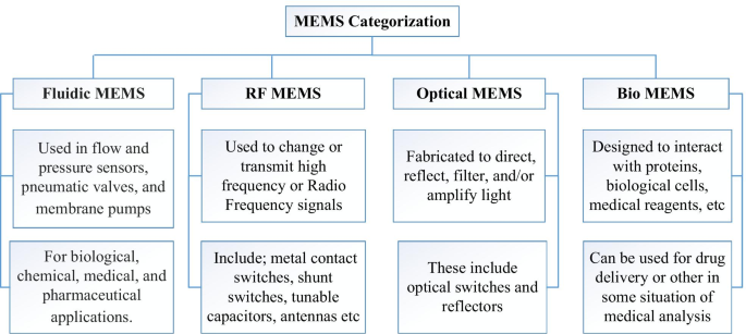
MEMS器件的分类
对于目前的大多数技术,MEMS 传感器是许多实际应用的首选新领域,从消费电子产品到航空工业。 MEMS 最重要的特点是能够与半导体芯片中的电子元件进行有效通信,传感器行业已经使用 MEMS 技术通过结合电子功能和机械动作[34] 发生了革命性的变化,它们通常具有低功耗和高灵敏度的特点。到小尺寸 [35, 36]。基于 MEMS 的传感器设备具有许多优势,使其在各种应用中发挥重要作用。这些优点包括由于阵列制造的潜力而导致的低成本 [37, 38]、低功耗 [37,38,39,40] 和小尺寸 [38,39,40,41,42]。此外,MEMS 还具有许多其他优点,例如重量轻、分辨率高、性能稳定以及易于与其他设备和系统集成。微机械到微机械设备的减少在几个领域得到了改进,例如,惯性传感器、化学传感器、喷墨打印机、陀螺仪、卫星、射频通信、智能手机、压力传感器、加速度计、生物医学仪器 [43]、军事应用、运动和力传感器 [44]。此外,制造过程的低成本和简单性在商业制造中起着至关重要的作用[45]。
根据工作原理,传感器设备可以根据工作原理分为两类:设备操作的静态和动态模式[46, 47]。当MEMS器件基于静态模式时,不包括频率信号。此外,由于表面吸附质量,梁会发生偏转,这将导致应力和结构变形的暂时结果。它可以通过压敏电阻的变化进行光学检测或感测。器件表面会产生一定的化学键,内部纳米力学可以弯曲MEMS光束检测[46]。在动态模式下,为了获得设备的最佳性能,应该激发机械谐振频率。振动系统所能达到并在特定系统中激发最大共振的最大振幅称为共振频率。其中共振频率受两个主要参数影响:梁的弹簧常数及其有效质量,并会根据这些参数发生变化。这就是利用共振频率的变化作为检测手段的工作原理。品质因数必须很高才能获得所需的灵敏度和分辨率 [48, 49]。由于它们是基于 MEMS 的设备操作和输出信号检测的基础,因此有必要了解和比较这些机制。
驱动技巧
驱动技术是一个术语,用于将输入能量转换为微结构运动的机制。驱动 MEMS 器件有不同的原理和方法 [7, 50,51,52,53,54,55],其中最重要的包括:静电驱动 [56,57,58,59,60,61,62, 63,64],电热驱动 [4, 44, 65,66,67,68],电磁驱动 [7, 69] 和压电驱动 [48, 70](图 2)。互补金属氧化物半导体 CMOS-MEMS 传感器器件设计用于使用平行板电容器的静电驱动或使用微加热器的电热驱动。另一方面,PolyMUMPs 和MetalMUMPs 传感器设备设计为通过使用嵌入式微加热器使用电热驱动[71]。
<图片>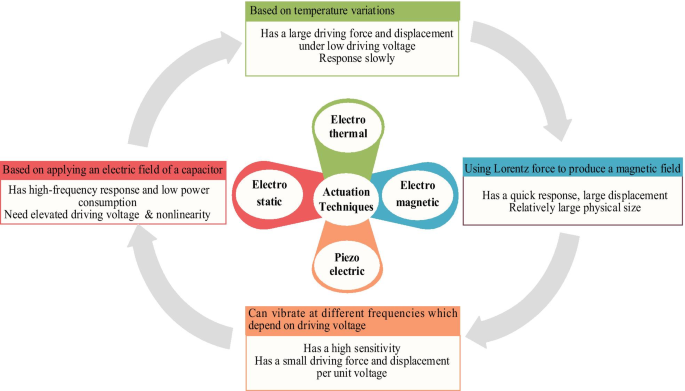
基于MEMS的传感装置的驱动技术
可以通过施加正弦力 F 来驱动基于 MEMS 的设备 (t ), 通过上述驱动方法之一。方程 (1) 用于求一般运动方程,因为 M 是顶板的总质量,b 是阻尼系数,k 柔性梁的弹簧常数,
$$M\ddot{\gamma } + b\dot{\gamma } + k\gamma =F(t)$$ (1)其中 F 表示 z 中外部驱动力的幅值 -方向,\(\ddot{\gamma }\)\(\ddot{\upgamma }\), \(\dot{\upgamma }\) \(\dot{\gamma }\) 和 γ 分别为质量的加速度、速度和位移。
静电致动器非常普遍;它们具有快速响应时间和低功耗 [72]。另一方面,使用电热原理的执行器很受欢迎;它们在低驱动电压下具有很大的驱动力和位移。电磁致动器具有响应快、位移大等优点。采用压电原理的致动器虽然单位电压的驱动力和位移小,但灵敏度高。因此,充分理解发生的原理对于获得具有这些驱动方法之一的高性能设备至关重要。
静电驱动
静电驱动的主要来源是电容器的电场,它依赖于两个带相反电荷的平行板之间的吸引力[12]。静电驱动基于库仑定律,该定律描述了在固定板和可移动板之间产生的具有一定距离的两个电荷之间的相互作用力。静电驱动被认为是驱动 MEMS 设备最流行的机制之一。它们具有简单的设计、快速的响应时间、易于制造和低功耗。然而,非线性和驱动电压的升高是这种类型的执行器的主要问题[72]。在静电驱动下研究 MEMS 时,必须仔细考虑某些类型的静电驱动。最流行的形式是基于由两个简单的平行板组成的电容器或由多个交叉或非交叉指组成的梳状驱动结构 [72, 73]。传统的方法[74]是平行板驱动,其中顶部移动板具有一定的极性,底部固定板具有相反的极性(图3)。动板的位移和振动取决于两板之间的电压差。当电荷极性相近时,定板和动板之间会发生排斥位移,但当两板带不同电荷时,动板会被固定板吸引。动板上电荷类型周期性变化时的驱动结果[50, 56, 74]。
<图片>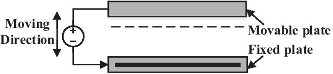
用于静电驱动的平行板电容器 [75]
当平行板被静电驱动时,拉入不稳定性是主要问题之一,因为固定板正好在微束下方,静摩擦会导致设备坍塌 [74, 76]。梳状驱动致动器由两组梳状指状结构组成(图 4)。它们通常放置在与基板相同的平行板中,其中一个梳齿固定在基板上,另一个连接到柔性结构(例如弹簧)以朝向和远离固定板移动 [72]。当在可移动梳齿和固定梳齿之间施加不同的电压时,边缘场的静电力通过固定的外部正弦力将两个梳齿吸引在一起。通常,平行板电容器在单位面积上比梳状驱动致动器更强,因为它们在致动器的固定板和移动板之间具有更大的重叠电容。然而,设计者更喜欢梳状执行器主要有两个原因:它产生较大的位移(几十微米可用),并且力与位移相对无关。总体而言,静电驱动在微机械驱动器 [77]、生物传感器应用 [56]、湿度传感 [57]、粒子和质量传感应用 [50、78]、MEMS 纳米定位系统 [58]、RF MEMS 开关应用 [ 13, 79]、MEMS 振荡器的闭环噪声 [60]、导航(汽车全球定位系统 GPS)[62、80]、陀螺仪 [81]、呼出气体中的生物标志物检测 [82] 和质量敏感气体传感器 [ 63]。此外,还报道了基于静电驱动和电容 CMOS-MEMS 的传感器装置用于无创糖尿病筛查的理论模型。其中糖尿病筛查是通过检测呼出气(EB)中的丙酮蒸气进行的,其中壳聚糖聚合物用作传感材料。具体而言,据报道,优化的灵敏度约为 0.042、0.066、0.13、0.18 和 0.26 pm/ppm [83]。
<图片>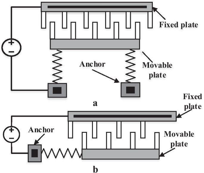
静电梳状驱动配置示意图 [84, 85], a 纵向交错梳状致动器; b 横向执行器
为了将 MEMS 器件激发到谐振状态或振动模式,必须通过在定子和转子的两个板之间施加交流电压来执行替代驱动。标准驱动模式如下所示[49]:简单的交流电压(V 1sinωt) , 直流偏置交流电压 (V 0 + V 1sinωt) 和推拉驱动(图5)。推拉驱动通常被认为是最好的解决方案,因为结构力可以施加到转子的两侧。推挽是一种适用于梳状驱动方案的理想驱动方式[49]。
<图片>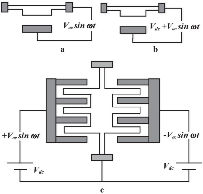
梳状驱动谐振器a 简单的交流电压驱动,b 带有直流偏置的交流电压,以及 c 推拉驱动方案[86]
电热驱动
电热技术主要用于 MEMS 驱动,而很少用于传感应用 [72]。电热技术本质上适用于灵活配置以产生具有所需位移的运动。由于对不同层的温差做出响应而产生的热力,由通过嵌入式微型加热器的端子施加的交流电流进行驱动[66]。微型加热器由不同材料层的组件制成,并在高温下运行。当施加交流电流时,器件温度升高;由于不同材料的热膨胀系数 (CTE) 不匹配,材料会膨胀,从而产生导致器件弯曲的热应力 [72]。另一方面,冷却方法可以通过传导到基板和对流到周围的空气(或液体)来实现。
这些温度变化以两种方式影响器件,如 [44, 87] 中所述:(1) 器件的尺寸变化或器件内部产生的应力,以及 (2) 器件的材料特性随温度变化。当前的技术需要压缩到微型加热器上。由于向电阻器施加特定电流,微型加热器会产生所需的热量,从而实现低功耗和快速响应时间。电热力可用式(2)[88]描述。
$$F_{th} =\alpha_{T} AE(T - T_{0} )$$ (2)其中α T 是 CTE, E 是梁的杨氏模量, A 是梁的横截面积, T 是最终温度, T 0为加热前的初始温度。几种材料已用于微加热器设计。例如,要实现最佳性能、精度、广泛的温度范围和稳定性,铂金和金将是微加热器的最佳选择 [89]。然而,它们是昂贵的[90]。在 MEMS 传感器中使用微型加热器需要一个内置温度传感器来将产生的热量转换为有用的输出。对于温度传感器,铂可在 − 200 ºC 至 800 ºC 温度范围内使用,镍可在 − 100 至 260 ºC 温度范围内使用 [90]。据报道,铝也是一种很好的温度传感材料[91]。图 6 显示了常见的电热驱动机制,包括 U 型梁执行器(热/冷臂)、双压电晶片执行器(双材料执行器)和屈曲执行器(V 型梁执行器或穿梭梁)。
<图片>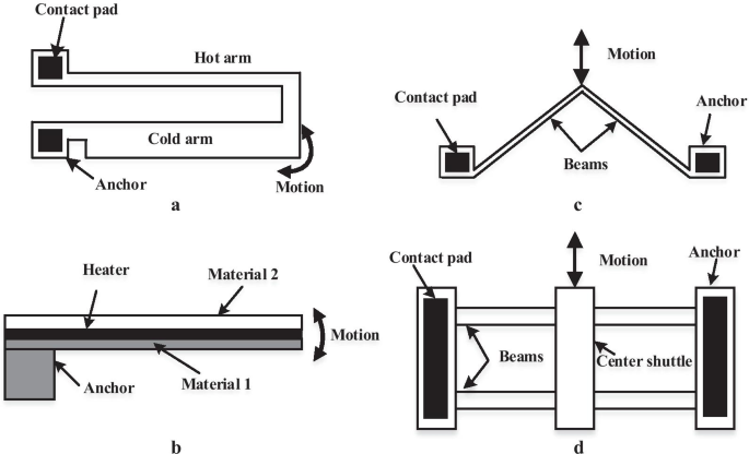
电热驱动原理图a U 型梁执行器(热/冷臂),b 双压电晶片执行器(双材料执行器),c 和 d 屈曲执行器(V型梁执行器和梭梁)[67, 92]
U 型梁执行器也称为热/冷臂,其中执行器由窄臂(热)、宽臂(冷)锚和接触垫组成 [67, 92]。它主要用于与基材进行平面或水平激发。这种技术的工作原理取决于在接触垫上施加差分电压,电流流过臂,热臂(电阻较高)比冷臂(电阻较低)加热更多的电流密度。因此,较窄的热臂比较粗的臂更热,并且会膨胀得更多。热臂会产生很大的热应力。两个臂之间的这种差异应变使整个设备偏转。
双压电晶片致动器,也称为双材料,由粘合在一起的两种不同的热膨胀材料组成。与前两个执行器不同,双压电晶片执行器 [93] 通常用于平面外驱动。当电流通过梁时,材料的温度升高。这个温度会使一种材料比另一种材料产生更大的膨胀,因为它具有不同的热膨胀系数,从而导致器件的热应力和弯曲。
热屈曲致动器由 V 形梁或梭形梁 [94]、锚固件和接触垫组成,它们也主要用于平面或横向驱动。当电流在梁之间流动时,由于发生焦耳热,梁温度升高导致热膨胀,这往往会膨胀并移动梭子或将器件的中心梁朝最简单且阻力较小的方向向前推动。
在实际实现中,大多数具有热驱动的 MEMS 器件在接近固有频率的频率下振动,因此计算器件的固有频率至关重要。电热技术由于其基于两层材料在极低激发电压下的热膨胀的大驱动力和位移而变得更加流行,当使用类似的测量时,这是无法通过任何其他策略实现的 [85, 95]。电热驱动具有多种优点,例如位移大 [95]、易于制造 [72]、力大和施加的电压相对较低 [52]。相反,它们需要大量电流和低电压放大器。此外,由于焦耳热,它消耗高功率。另一个限制是对环境温度的敏感性。最后,由于电热驱动而增加的激励温度和热量会随着系统的封装阶段而导致相邻电子设备的几个缺点[72]。
已经开发和研究了多种类型的电热驱动;热/冷臂 [96,97,98],双材料或双压电晶片 [98, 99] 和热屈曲致动器 [98, 100]。参考文献 [101] 研究了使用双压电晶片执行器在热驱动下的微悬臂梁振动。参考文献 [102] 提出了使用 MUMP 工艺制造的多晶硅微环热驱动 (RTA) 的结构化程序。设计了一种基于热驱动的微悬臂梁。他们假设系统处于真空或流体(气体)液体中,并提出了一个分析解决方案 [103]。丹尼斯等人。 [44] 使用二氧化钛 (TiO2) 纳米粒子作为传感材料,制造了一个 (CMOS-MEMS) 系统,内置微型加热器在相对较高的温度 (40–80 °C) 下运行,以测量湿度水平。该传感器使用电热驱动在动态模式下运行,并使用连接到惠斯通电桥电路的压阻 (PZR) 传感器评估输出信号。随着湿度从 35% RH 增加到 95% RH,湿度传感器输出电压从 0.585 mV 增加到 30.580 mV。 The sensitivity of the humidity sensor increases linearly from 0.102 mV/% RH to 0.501 mV/% RH with an increase in the temperature from 40 to 80 °C and a maximum hysteresis of 0.87% RH is found at a relative humidity of 80%. In a further notable contribution, Almur et al. [104] modelled a MetalMUMPs acetone vapour sensing system based on electrothermal actuation and capacitive sensing. The output voltage change was found to increase linearly with increasing the acetone vapor concentration from 100 to 500 ppm with a concentration sensitivity of 0.65 mV/ppm. Due to the thick nickel layer of the MetalMUMPs technology used the device has very high mass (4.7 × 10 –8 kg) and low mass sensitivity (0.118 MHz/pg).
Electromagnetic Actuation
The electromagnetic operation has long been utilized in the sensing and driving of the large scaling applications (such as loudspeakers). This technique demands electricity to stimulate the magnetic effect. It uses the electromagnetic force (also can be called Lorentz force after the Dutch physicist Hendrik A. Lorentz 1895) to produce a magnetic field to the resonator by applying an alternating current on the coil or inductor integrated into the resonator (Fig. 7). Lorentz Force is defined as the force generated on a point charge as a result of the combined electric and magnetic forces on the charge [72]. Electromagnetic actuation has also been utilized as a guide to other actuation techniques, for example, electrostatic [33] and electrothermal [34]. In this technique, when a conductor conveying an electric current I can be applied to an external magnetic field B , this will induce a Lorentz force F L as stated by (3) [72].
$$\vec{F}_{L} =L\vec{I} \times \vec{B}$$ (3)其中 L indicted to the conductor length and × refers to the cross product operation. The current in the conductive element located within the magnetic field generates an electromagnetic force in a direction perpendicular to the current and the magnetic field. This force has a directly proportional to the current, magnetic flux density and length of the microbeam. Because of the interaction generated by the current between the magnet and the magnetic field, a mechanical displacement on the microbeam will be generated as a result of the applied current to the micro-coil. For example, electromagnetic actuation has been used to stimulate microbeam when being exposed to an external magnetic field by flowing current through the microbeam, as seen in Fig. 7a. Similarly, as alternating current flows through the device on the microbeam, this approach can be used to excite the out-of-plane resonator (Fig. 7b). Lorentz forces of equal value and opposite directions are produced if the coil is deposited on a structure of the microbeam. The opposite directions of the current flowing through the different parts of the coil correspond to these forces. Such forces balance one another out. Figure 7c, however, can induce a net motion that is used to actuate the microbeam [72].

Schematic of the electromagnetic actuation using Lorentz forces a in-plane actuator, b 和 c out-of-plane actuator [72]
The electromagnetic technique involves many merits over the other kind of actuation techniques. The main advantages of the electromagnetic actuation include the large displacement without the influence of the nonlinear effect [105], lower voltages due to they based on current rather than voltage-driven [7], in addition, they have a high reproducibility rate, they also have more features like rapid response, high accuracy, and the merit for controlling easily. For MEMS applications, the electromagnetic technique is the best choice to achieve maximum driving force for device size ratio [106]. However, they still suffering from some drawbacks due to using the huge current resulting in high power consumption, also their fabrication is complicated (normally be in need of inductive parts to produce magnetic flux also the possibility of including the manufacture of coils, and the deposition of a magnetic material) [7]. This fact combined with constructive difficulties has limited magnetic actuation applications. However, there are successful application examples in the literature as it may exist in MEMS switches devices [7], Optical switches, and micro scanners [69], gyroscopes [107], or relays [108]. Many researches are also based on magnetic actuation [109]. The magnetic microsensors utilizing the commercial 0.35 μm CMOS process has been investigated [110]. In a further contribution, Barba et al. [111] designed an electromagnetically actuated MEMS cantilevers proposed in order to minimize parasitic phenomena using Boron-doped silicon. In another seminal work, an electromagnetic and Piezoelectric actuated and piezoresistive sensed CMOS- MEMS device has been modelled for humidity sensing using ZnO NRs (6 μm/chitosan SAMs) as a sensing material [83]. The sensitivity was found to be 83.3 ppm [112].
Piezoelectric Actuation
Piezoelectric effect indicates the capability of a particular material to produce an electrical voltage in response to applied the mechanical stress. Piezoelectricity was discovered by the Curie brothers in 1880, and 'Piezo' meaning is coming from the Greek word that is mean 'press' or 'push'. A piezoelectric actuator defined as transducers that converts an applied potential into a mechanical movement or strain based on the piezoelectric influence [72]. Piezoelectric materials like quartz, zinc oxide, lead zirconate titanate (piezoelectric ceramic material PZT), and polyvinylidene difluoride (PVDF) are commonly used in sensor and actuator applications on a macro scale as well as in MEMS applications in recent years, but the sensing is limited due to their lack of a DC response [49]. Piezoelectric materials act electrically as insulators and required to be placed between two conductive electrodes so as to gather charge or to apply an electric-field (using an interdigitated electrode or sandwich structure) [113].
In MEMS devices, the basic principle of the piezoelectric actuation method is based on using a thin piezoelectric layer that is deposited as a part of the MEMS beam between flexible (Fig. 8). When a voltage is applied to the piezoelectric layer, the piezoelectric material expands according to the polarization of the applied voltage, which causes an axial bending across the length of the flexible beam [114].

Schematic of the piezoelectric actuator [72]
In general, piezoelectric actuators exhibit a lot of advantages such as high output force, good operating bandwidth, very compact size, lightweight, low power consumption, and fast response [114, 115]. Their characteristics are well known and have been used for decades. Most first sensors use piezoelectric actuation and are still in use today. However, small displacements of actuators are a major drawback, and their high-temperature sensitivity [72], nonlinear working area and hysteresis limit their wide range of applications [49]. Piezoelectric materials are very brittle. They can seldom be utilized alone but are often connected to a flexible structure for actuation and sensing applications. There are several works based on piezoelectric actuation [2, 48, 114, 116] studied the prospective to use a piezoresistive microcantilever for environment application, particularly for humidity sensing. Mahdavi et al. [117] proposed a new class of accurate dew point measurements taking advantage of thin-film Piezoelectric-on-Silicon (TPoS) resonators using ZnO NRs (6 μm/chitosan SAMs). The sensitivity was found to be 16.9–83.3 ppm at the range of response time of 46 s/167 s. sensitivity to mass loading based on piezoelectric excitation is investigated for chemical sensing [118, 119] reported piezoelectric transduction of flexural-mode silicon resonators to achieve efficient temperature compensation. The resonance gas sensor using piezoelectric MEMS for defence applications was reported [120].
Actuation Techniques Discussion
Different types of MEMS actuators require different drive electronics. As per mentioned in this article, there are different principles and approaches to actuate MEMS devices. The most important of which include:electrostatic actuation, electrothermal actuation, electromagnetic actuation, and piezoelectric actuation. Electrostatic actuators are a traditional field and considered one of the most popular mechanisms for actuating MEMS devices. They have a simple design, fast response time, ease of fabrication and low power consumption. However, the non-linearity and the elevated value of the driving voltage is the major matter of this type of actuator. Electrothermal actuators provide very low resistance to their drive sources and require high currents rather than high voltages to move them. High voltage amplifiers are not particularly suitable for use in electrothermal MEMS actuators. Instead, a low voltage and high current signal source are required. Of course, this can also work if the output current of the high voltage amplifier is large enough to drive the electrothermal actuator, but it is not a particularly energy-efficient or cost-effective solution. For MEMS applications, electromagnetic technology is the best choice to achieve maximum driving force per device size ratio. However, they still suffering from some drawbacks due to using the huge current that results in high power consumption, also their fabrication is complicated (normally be in need of inductive parts to produce magnetic flux also the possibility of including the manufacture of coils, and the deposition of a magnetic material). Piezoelectric actuators also required high voltage amplifiers, but since they are typically used for resonance, the drive requirements in terms of driving voltage are typically lower than those required for other actuators. The recent research of MEMS-based sensor devices which can be actuated using the four basic actuation techniques that have been used during the last few years for many applications, as shown in Table 2. It can be clearly observed that there is a rising development pattern in the field of micro-assembly and micromanipulation for MEMS-based sensor devices that have been categorized based on actuation techniques. Nowadays, a wide range of applications has been identified for MEMS-based sensor devices that provide high sensitivity and resolution. The sensing systems are getting more robust and reliable due to the integration configuration.
Sensing Mechanisms for the Output Signal
The sensing mechanism is used to sense the output of the MEMS devices. The basic of the sensing technique is based on the use of a polymer deposited on the sensing layer of the device to absorb a particular chemical that creates a variation in the stress, mass, electrical or mechanical characteristics of the beam. To estimate the change in the mass, the resonant frequency of the device can be measured based on the detected mass increment that is one of its parameters. Then again, when the polymer absorbs the mass, piezoresistor that is situated on the surface of the sensing element can be used to estimate the mass of the beam. Another method of detecting suspected chemicals is to use thermocouples to measure temperature changes caused by the heat generated by the polymer absorbing analyte [49].
To sense the output of these MEMS devices methods such as piezoresistive, capacitive or optical mechanisms are used (Fig. 9) [123]. Different sensing mechanisms have different advantages and disadvantages at the same time.

Sensing mechanisms of MEMS-based sensor devices
For instance, optical sensing has good feasibility; however, it is very expensive to implement compared to capacitive and piezoresistive techniques [124]. Capacitive and piezoresistive techniques are the common methods used to sense the output signal. CMOS- MEMS device was designed to encompass both piezoresistive and capacitive sensing techniques due to the features of 0.35 µm CMOS technology used to design it. In contrast, PolyMUMPs and MetalMUMPs devices were designed to use only capacitive sensing techniques.
Piezoresistive Sensing
Piezoresistive is a common sensing principle used in MEMS devices. Essentially, the principle of piezoresistive materials is based on the resistance change when their strain changes in response to applied stress. This change can be observed in the electrical resistance of the material of the device as a consequence of a surface-stress change due to bending. The resistance value of the piezoresistor with the resistivity ρ of a resistor, length of l and cross-section area A is given by (4) [29].
$$R =\frac{\rho l}{A}$$ (4)The change ΔR in resistance is proportional to the applied strain can be defined in (5) [29, 125].
$$\Delta R =G\varepsilon R$$ (5)where G is the gauge factor work as a proportionality constant of the piezoresistor, ε is the strain in the material, and R is the piezoresistor resistance. A piezoresistive element behaves differently towards longitudinal and transverse strain component presented by [29]. According to (5), the resistance of a piezoresistor can vary owing to the changes of the geometry (length and cross-section) or in the property of the material (resistivity). Piezoresistive detection depends on the difference in resistivity of material when stress is applied. In a piezoresistive material, the change of resistivity because of the application of stress has a much greater effect on the resistance than the change in resistivity because of a change in the geometry (sensors rely on the change of resistance owing to the geometry are so-called strain gauges) [72]. (Fig. 10) shows different resistor orientations and external force loading directions [88].

一 Longitudinal piezoresistance dominates, b 和 c transverse piezoresistance dominates presented [29]
The main drawback of this sensing mechanism is the solid temperature reliance of resistivity. To limit this impact, normally, a collecting of four piezoresistive designed is utilized to shape a Wheatstone bridge. This limits the temperature reliance [72]. Furthermore, the small changes in the electric signal generated from gauges are translated and gauged as voltages utilizing this Wheatstone bridge [49]. Wheatstone bridge utilizes four resistors arranged in the bridge of the four arms (Fig. 11). Based on the quantity of these active resistors (acting as a transducer), single active bridge (single transducer), half active bridge (double transducers), and the full active bridge (quadruple transducers) of the bridge of Wheatstone might be utilized as reported [72]. The single active bridge as well called Quarter Bridge that utilizes just a single active component which changes because of a physical ambient, for example, pressure, power, temperature, while the remnants of that resistors will be passive and so on. MEMS systems have been used as temperature, calorimeter, and in combination with the Wheatstone bridge, sensors allow the base fluctuations. Thermal bridge system is one of the best-known sensing platforms among MEMS. In the AC-driven Wheatstone bridge configuration (Fig. 11b), researchers have utilized the resistance-based thermometry to analyse temperature changes with micro-Kelvin resolution. In an overview, the right half of the bridge comprises a sensing resistor on the lower branch with associated resistance on the top, while the left side is defined as the matching one. Fixed resistors with a relatively low resistance coefficient of temperature are used with resistance values, which was chosen to enhance stability and resolution based on the previous study [126].

Schematic types of a Wheatstone bridge, a quarter bridge, b half-bridge, and c full-bridge configurations [72]
Silicon piezoresistor and polysilicon patches are generally utilized in MEMS sensors. The resistivity of silicon relies upon its strategy for doping. N-type doped with silicon is less sensitive than p-type. This raises limitation to the fabrications. In this situation, an in-plane transversal and in-plane longitudinal will be the most significant elements [72]. For semiconductor materials like silicon, the longitudinal and transverse gauge factors owing to geometry change are quite tiny compared to their values due to resistivity change, hereafter the change in geometry can be ignored, and the longitudinal and transverse gauge factors due to only the resistivity change are found using (6) and (7), respectively [127].
$$G_{L} =\pi_{L} E$$ (6) $$G_{T} =\pi_{T} E$$ (7)其中 E is Young's modulus of the piezoresistive material. π L and π T are the longitudinal and transverse piezoresistance coefficients, respectively, for arbitrarily oriented polysilicon grains, and their values are given in Table 3 [19].
Currently, the piezoresistive effect has been utilized as a bio-or chemical detection [48], humidity sensing purpose [4], switch applications [59], biomarker detection in exhaled breath [82], micro scanners [69], pressure sensing [128], and mass-sensitive gas sensors [63]. Zope et al. [117] developed a resistively sensed thermally-driven piezo resonator composed predominantly of CMOS material for mass sensing applications. whereas mass sensitivity of 24.96 kHz/ng was reported. The extracted mass resolution of 16.3 fg have also been observed, hence showing great potential to serve as an aerosol sensor).
Capacitive Sensing
The capacitive sensing mechanism is based on measuring the changes of the capacitance between the stator and rotor fingers or between the fixed plate and movable plate [88]. Capacitive sensing is the main dominant method for micromachined applications due to its compatibility with all the fabrication approaches and stiffness [129, 130]. Capacitive sensing has many attractive features include high sensitivity, low power consumption, simplicity in design, low drift and low-temperature dependency. Furthermore, the measurement of the output signal can be easily fabricated on the PolyMUMPs die using capacitive sensing. Only a single parallel plate can be used to capacitively sensed the variations in the natural frequency or amplitude of the MEMS devices (such as a CMOS-MEMS device and a PolyMUMPs device) or by applying a comb finger (such as a MetalMUMPs device).
For CMOS-MEMS device and PolyMUMPs devices, when there is no actuation (Fig. 12a), the initial static sensed capacitance (Cs0) between the lower fixed plate and the movable top plate is calculated using (8) [19].
$$C_{s0} =\frac{{\varepsilon A_{s} }}{{z_{0} }}$$ (8)where ℇ is the relative permittivity of the dielectrics, As is the area of the sensed plates and z0 is the gap between the fixed and movable plates. When the movable plate is displaced by z (Fig. 12b) the initial gap changes, and hence the capacitance will change too, and it is found by (9).
$$C_{s} (z) =\frac{{\varepsilon A_{s} }}{{z_{0} - z}} =C_{s0} \frac{{z_{0} }}{{z_{0} - z}}$$ (9)
Parallel plate capacitor showing a initial condition and b after displacing the movable plate [19]
At the same time, for the MetalMUMPs devices, the output can be detected capacitively by utilizing the differential comb fingers design. As appeared in Fig. 13, there are two arrangements of fixed comb fingers to have the differential capacitance.

Comb fingers configuration for MetalMUMPs device showing a the initial condition and b the displacement of the vibrating comb finger [19]
For the initial condition, when the device is not actuated (Fig. 13a), the static detected capacitance C0 for every set of vibrating-fixed fingers could be calculated by (10).
$$C_{0} =n\frac{{\varepsilon l_{f} w_{f} }}{d}$$ (10)where l f and w f are length and width of the overlapping area of the vibrating and fixed comb fingers, respectively. d is the gap between the fixed and vibrating comb fingers and n is the number of the vibrating comb fingers. When the device is moved by y toward the fixed comb finger one as appeared by (Fig. 13b), the capacitances C 1 and C 2 will be changed and relying upon that shift, and their values can be calculated using (11) and (12), respectively.
$$C_{1} (x) =n\frac{{\varepsilon l_{f} w}}{d - y}$$ (11) $$C_{2} (x) =n\frac{{\varepsilon l_{f} w}}{d + y}$$ (12)The output signal of the device will be measured as a voltage due to change in the sensing capacitance upon actuation using MS3110 capacitive readout circuit that translates the change in capacitance to the output voltage change in response to the temperature of the microheaters. Nowadays, capacitive effects are used in MEMS resonators [60], biosensor application [56], humidity sensor [57], diabetes screening [66], Navigation (automobile Global Positioning System (GPS)) [62], a low noise accelerometer [131], and RF MEMS capacitive switches [132].
Optical Detection
Optical sensing mechanism depends on detecting the changes in the transmitted light compared to the received light. The detection of compound species by spectral transmission strategy is broadly acknowledged. Optical sensors are notable due to their selectivity since it does not rely upon any chemical reaction or any chemical catalyst activities. Air pollutants identification is recognized by using the characteristics of the optical species (for example, absorption, refractive index, Raman scattering, fluorescence, and reflection). Optical sensors utilize emission and absorption measurements primarily through different technologies such as Fourier transform infrared spectroscopy (FTIR), surface plasma resonance (SPR), differential optical absorption spectroscopy (DOAS), laser diode absorption spectroscopy (LDAS), cavity ring-down spectroscopy (CRDS), non-dispersive infrared (NDIR) spectroscopy, light detection and ranging (LIDAR), UV fluorescence and chemiluminescence for the sensing of air pollutants in air specimens. Normally, the light will be cross through, modified or reflected by some space having the relevant medium (Fig. 14). Beer–Lambert law can be used to govern the optical detection of the air pollutants as per the following:
$$I =I_{0} *e^{ - \alpha l}$$ (13)where the transmitted light through the specimen is I , I 0 is the received light, α represent the absorptivity, l represents the length of the path.

Schematic representation of an optical MEMS sensor [133]
However, the majority of the applications for optical MEMS are in communications; there are various uses in different fields [134]. The literature covered numerous attempts to introduce the optical detection of air pollutants. A few of these sensors are used to recognize chemicals. This displays the multifunctional part of these sensors. Infrared spectrometry is a case of a technique that can be utilized for optical sensing [135]. In a further notable contribution, Huang and co-workers have also demonstrated [136] the simulation of an integrated optical MEMS accelerometer. The effective simulation results have demonstrated as follows:a resonance frequency of 562.85 Hz, a mechanical sensitivity of 781.64 nm/g, an optical system sensitivity of 1.23, a resolution of 1.037 µg, and low cross-sensitivity. The proposed accelerometer can be used for improvements in MEMS inertial navigation devices. Another model is the Fabry–Perot optical sensor [137]. Basically stated, the principles of this sensor are based on bringing gas into a chamber and a short time later going light through the chamber. Due to changes in the substance piece, the light experiencing will be not exactly equivalent to without the gas. This light is broke down, and from the results, confirmation can be made about the sort of gas being tested. The fruitful testing of an optical MEMS sensor for the location of catechol was reported [133]. The absorbance measurement of catechol oxidation was performed by blue light (472 nm) attached through a MEMS device. The light was transmitted from a free-space blue laser working in persistent wave mode and is focused on a multimode fibre utilizing manually arranged to organize. Received light was coupled by means of the optical fibre to a USB connected spectrophotometer which assisted computerized information collection utilizing the software.
Sensing Mechanisms Discussion
In view of different working principles, the above-mentioned sensing mechanisms can be divided into three types, namely piezoresistive, capacitive and optical mechanisms. There are benefits and drawbacks for different sensing mechanisms at the same time. For instance, optical sensing has good feasibility; however, it is very expensive to implement compared to capacitive and piezoresistive techniques. As a result, piezoresistive and capacitive techniques are the common methods used to sense the output signal. Any small change in the stress could be detected using a piezoresistive technique. A main disadvantage of the piezoresistive sensing technique is the high-temperature reliance of resistivity. In Table 3, present the recent work and progress (last 5 years), including actuation and sensing mechanisms, sensing materials, fabrication technology and application. The miniaturized microchip presented (in Table 4) can be utilized for gas and humidity sensing, human health screening, inertial navigation with good repeatability, high resolution, high sensitivity, and rapid response. In addition, MEMS sensors have been proven to be an effective medium for sensors combined with on-chip electronic circuitry. It can therefore function not only as a portable sensor chip but can also be linked as part of the Internet of Things (IoT) network to achieve real-time and remote high-sensitivity moisture tracking.
Discussion
Recent developments are about new technologies that can harvest energy from the environment, because sustainable self-sufficient micro/nano power sources are an emerging field of nanoenergy, which involves nanomaterials and nanotechnology when harvesting energy for powering micro/nano systems [139]. The triboelectric charge is produced only on the surface dependent on the physical friction between two separate materials. The triboelectric nanogenerator (TENG) is a device that transforms mechanical energy into contact separation or relative sliding between two materials with opposite polarities. TENG based on the coupling effect between triboelectricity and electrostatic induction in which it’s updated progress and potential applications as new energy technology and as self-powered active sensors. The suggested approach uses biomechanical energy transfer to electricity from human activity [139, 140]. Amongst them is a successful study has been investigated for the conversion to wearable energy from portable biometric devices and self-powered sensors based on triboelectricity (i.e. the charge produced on the touch surface) [141,142,143,144].
-
To decrease power consumption during operation, sensors of woken up or almost zero-power supplement need to proposed and investigated, meaning that these sensors do not have any energy consumption. With these components of MEMS, MEMS sensors can work for a long period or can be operated in a self-powered.
-
Looking forward to the future-oriented sensors, sensors with flexibility have become hot topics of the recent research in the latest years owing to their versatility and great prospective in health/human beings applications. Flexible sensors are often used in combination with wearable sensors to have their unique advantages. More than just utilizing the flexible sensor such as a wearable electronic for observation functions, they can be even utilized as a human–machine interface for achieving higher requirements. With the enhancement of the quality of human life, wearable devices and human–machine interfaces have been recognized as important directions for developing sensors of the future with sufficient flexibility and versatile sensing capabilities. Wearable electronic devices can be simply integrated with the human body to extend our perception capabilities. Sensor functions of wearable electronic devices include, but are not limited to, force, strain, electrophysiology, heart rate monitors, temperature, fitness trackers, etc. With the service of various devices among different anatomical positions, development of many applications of the human body sensor can be facilitated from hospital care to fitness and wellness tracking, human–machine interfaces and recognition and assessment of cognitive states.
-
Meanwhile, by combining MEMS sensor with artificial intelligence (AI), the next generation of sensors will provide clear evolutionary impact and help humans interact with other things in various applications circumstances. Moreover, the quick improvement of the modern community has observed the expanding association among people with machines, demanding huge intelligent human–machine devices. Around a huge data and hypersensitive detecting, MEMS sensor utilizing a machine learning strategy dramatically stimulates the enlargement of the coming generation smart sensing system. This interactive system with next-generation sensor provides consumers with a more comprehensive experience. It can be used for many practical applications, such as simulation of sports training, entertainment, medical rehabilitation and so on.
Conclusions and Future Trends
It is well recognized that MEMS-based sensors play a key role in the field of miniaturization and electronic microcircuits. It is necessary to understand and compare these mechanisms since they are the basis of the MEMS-based devices operation and output signal detection. This article reviews several popular actuation and sensing mechanisms related to MEMS devices that have emerged over the past few decades. This article introduced a descriptive overview to the advancement of the actuation and sensing mechanisms of the MEMS-based sensor devices. The up-to-date trends and the restrictions while giving a valuable perception into the field of emerging actuation and sensing technologies. A comprehensive discussion was presented, underlining the significance of the actuation and sensing mechanisms, its structure, working principles, classification, fabrication and applications. Proper understanding of the actuating and sensing mechanisms for the MEMS-based sensor devices play a vital role in their selection and effective application in various innovative technologies. In addition, the proper selection of actuating and sensing techniques in MEMS sensors based on the desired application such as sensitivity, resonant frequency, input\output voltage, temperature etc., will lead to fast-commercialization and better product stability.
In order to perform various tasks for different applications such as industry and electronic equipment, different MEMS devices with different structures collaborated with diverse actuation and sensing mechanisms will arise in true-life. Moreover, MEMS devices will not only be used for simple tasks, but also for more jobs that are complex. At the same time, MEMS devices will have greater freedom and can meet the needs of a variety of applications. However, in order to pursue higher accuracy and miniaturization, the complexity of MEMS device design will continue to increase. In addition, MEMS products have a close relationship with the market. It can be predicted that MEMS devices will realize more functions, miniaturization and low cost, which is a huge challenge for other products. Therefore, in the next few years, MEMS fabrication approaches will develop to a higher level to meet market demand. With the advancement of MEMS device fabrication processes, unique hardware makers will seek after shorter fabrication cycles and quicker fabrication speeds.
One of the central areas of the future trend in this area is reliability research and improvement methods. Moreover, new materials and cost-effective of the fabrication techniques will provide important opportunities for development. It has been demonstrated that the design capability is not limited to standard principles and can improve qualitative performance. Despite MEMS advantages, few challenges still exist in the following aspects.
-
The traditional MOS thin films by MEMS techniques often show poor sensitivity to target gases due to the compact surface structure and low crystallinity.
-
In recent studies, it have tried to integrate high-performance MOS nanomaterials onto microheaters. Still, it is difficult to control and cast the slurry-based MOS nanomaterials onto the suspending heating area of microheaters. However, the low yield and large device-to-device deviation hamper the sensor fabrication on a large scale.
-
It is also complicated to improve the adhesion between microheaters and sensing materials to get stable parameters, especially at high temperatures > 350 °C which results in decreased sensing performance and low stability [14, 145].
-
Fabricating sensing films with high sensitivity using MEMS compatible methods is an urgent goal.
-
Towards a new era, different challenges can face MEMS-based sensors in terms of power supply and intelligence during the operation, such as the challenges of the flexibility of wearable applications, the friendly interactive capabilities of human–machine interface applications, and analysis of the huge data.
数据和材料的可用性
不适用。
缩写
- MEMS:
-
Microelectromechanical system
- pH:
-
Potential hydrogen
- ICs:
-
Integrated circuits
- LOD:
-
Limit of detection
- MUMPs:
-
Multi-user MEMS
- MST:
-
Microsystems technology
- RF:
-
Radio frequency
- CMOS:
-
Complementary metal oxide semiconductor
- CTE:
-
The coefficient of thermal expansion
- AC:
-
Alternating current
- DC:
-
Direct current
- RTA:
-
Ring thermal actuation
- PVDF:
-
Polyvinylidene difluoride
- GPS:
-
Global positioning system
- FTIR:
-
傅里叶变换红外光谱
- SPR:
-
Surface plasma resonance
- DOAS:
-
Differential optical absorption spectroscopy
- LDAS:
-
Laser diode absorption spectroscopy
- CRDS:
-
Cavity ring down spectroscopy
- NDIR:
-
Non-dispersive infrared
- LIDAR:
-
Light detection and ranging
- IDE:
-
Interdigitated electrodes
- PZR:
-
Piezoresistive
- EFS:
-
Electrostatic field sensor
- AI:
-
Artificial intelligence
纳米材料