

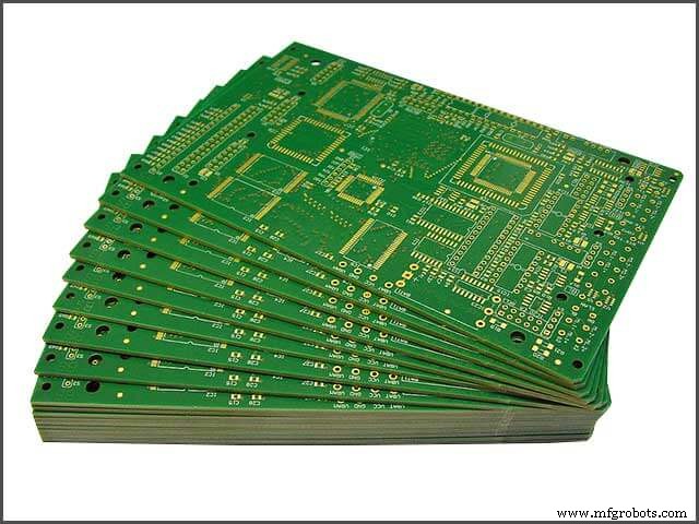
从面包板 PCB 原型到完整产品的指南
从面包板 PCB 原型扩展是一个复杂的过程,它结合了创造力和程序。开发时间表与运行项目的人一样独立,一切都始终掌握在创作者的手中。然而,在此过程中,有几个里程碑需要寻找。面包板PCB
https://youtu.be/HAOvEPh8hms
开始构建您的 PCB 原型
所以现在你有了这个奇妙的想法,或者更好的是,PoC(概念证明),但你需要扩展到值得大规模生产的东西,或者至少可以由一些制造商制造用于演示目的;您如何开始构建您的 PCB 原型?
在硬件设计中,PCB 原型是一种“手工构建”模型,代表了制造(易于复制)的产品,足以让设计人员可视化和测试设计。原型一词来源于拉丁语proto,意思是原始,类型,意思是形式或模型。
有了所有教程和可用的免费资源数量,几乎任何人都可以在几个小时内构建快速的 PCB 原型。将您的 PCB 原型带到可以商业化的地方需要大量的努力、规划和一些专业知识。你必须做出一系列关于硬件的决定,最终推动关于设备软件的决定。面包板PCB
使用 Raspberry Pi 甚至流行的 Arduino 很容易构建,但使用它们进行大规模生产的机会大多是有限的。当然,这并不意味着你不可能像 Arduino Pro Mini 那样在 Arduino 板上构建一个板,或者那些无头 Arduino 可以插入然后继续制造类似的东西。不过,它们可能会变得非常昂贵,甚至可能比您需要的更强大。
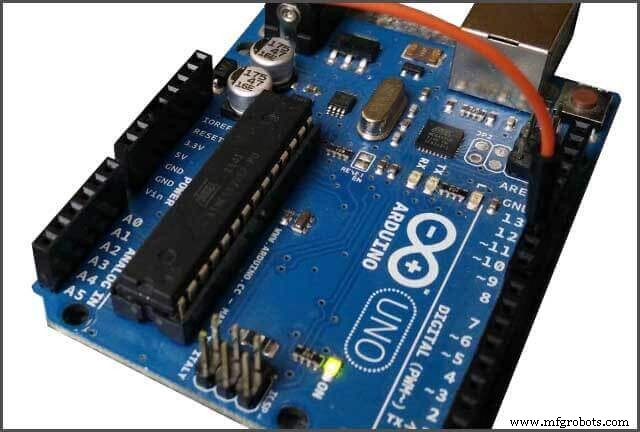
当今的许多硬件初创公司都使用 Arduino 构建了他们的第一个 PCB 原型 . 阿杜诺 即使没有电气工程背景或只有必要的编程技能,也易于学习。即使是孩子也能做到,而且他们中的很多人都做到了。
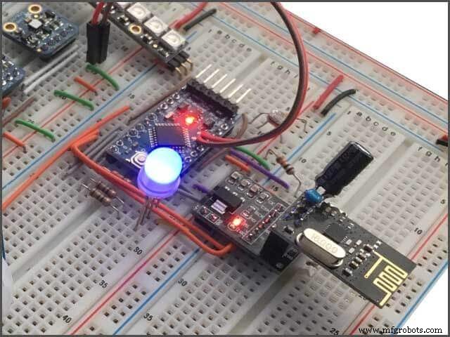
1.1 面包板PCB —组件选择
开始构建 PCB 原型的第一步是了解您需要哪些组件。您可以根据您的框图或现有的 PoC 快速了解这些内容,甚至设备所需的功能也可以迅速说明这一点。例如,构建可穿戴式心跳监测器之类的东西 将需要以下一些:
1. 微控制器单元——Atmega、ARM、PIC 等
2. 脉搏传感器 - 可以使用专用的脉搏传感器,或者 LED 和光检测器的组合也可以工作。
3. 供电单元
4. 显示接口——LCD、LED、OLED、TFT等。
人们可以轻松地将大部分(如果不是全部)所需的零件外包给一个电子供应商,在某些情况下,外包给多个供应商。以下是一些您可以从 AliExpress、Digi Key、Arrow、Mouser、Adafruit 等处购买详细信息的供应商。
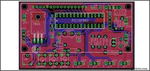
1.2 原理图设计
下一步是创建电子设计图,通常称为示意图 或电路图。示意图显示了每个组件是如何连接的,这不是你会用手做的事情,而是为此目的而设计的独特工具。
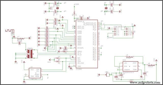
创建原理图是构建最终设备的核心步骤,您不能跳过它。开始使用您的架构非常容易;您需要知道正确的构建工具。有几种电路设计软件可用于原理图设计,有些是免费的,有些是付费版本。大多数设计软件都可用于绘制原理图,也可用于制作 PCB 布局。
以下是一些要使用的软件:
1. KiCAD – 免费使用。
2. Eagle CAD – 高级版,但免费选项有限
3. Altium – 高级版
4. DipTrace - 高级
5. OrCAD – 高级版,但提供免费试用。
确定要使用的设计软件后,可以熟悉软件环境,因为每个软件的外观和感觉可能不同。
在您选择的软件上创建原理图时,必须遵循一些原理图设计的标准做法。
下面重点介绍一些常规方法——
1. 使用连接点表示连接在一个连接处的多个连接。
2. 为引脚使用网络名称,而不是在周围绘制数百个连接。这样做可以增强原理图的可读性,而不会增加任何不必要的混乱。
3.同一设备始终使用相同的符号
4. 将你的架构分成逻辑块,尤其是在设计一些复杂的电路时。
当您完成原理图设计并对其进行全面交叉检查后,下一步就是将电路设计转换为制造 PCB;布局失败的可能性很高,这可能会对最终产品的功能产生负面影响。将使用几种 PCB 布局来制造您的电路板。
在下一章中,我们将讨论为您的 PCB 原型制作印刷电路板。
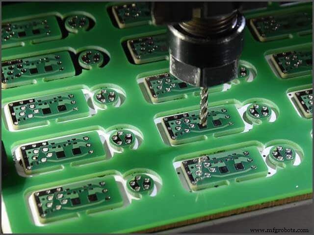
为您的 PCB 原型制作印刷电路板
为您的 PCB 原型制作印刷电路板,首先,拥有原理图是拥有成熟专业电路板过程的一个步骤。
该过程的下一阶段是不能跳过的,即设计印刷电路板的布局。但是,什么是印刷电路板?
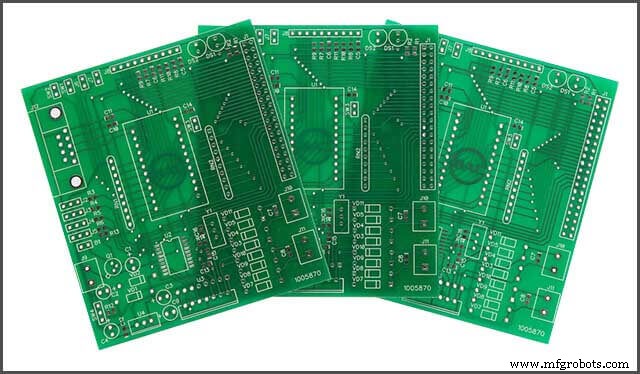

A 印刷电路板 ,也称为 PCB,是一种物理板,可将所有电子元件固定并连接在一个位置。通常使用多种方法将原理图设计转移到 PCB。 PCB的设计会影响一些因素,如
1. 成本——板子越重要,制造成本就越高。
2. 性能——电路板设计和使用的组件类型会影响设备的整体性能。设计不佳的电路板可能容易受到噪音的影响,从而降低设备的性能。
3.耐用性,
4. 还有更多。
一旦原理图准备好,我们就开始制作PCB。
PCB的设计与创建原理图时使用的软件相同。
该软件将负责根据给定的组件和原理图生成 PCB 布局和封装;如果没有原理图,软件将无法创建基本的 PCB 布局。
对于初次使用的用户来说,开始制作 PCB 布局可能既耗时又乏味。不过,幸运的是,大多数 PCB 软件都有一些方便的在线教程和资源来学习如何构建它们。
根据选择的软件,用户通常可以通过一种方式从原理图视图切换到 PCB 布局视图,在该视图中设计 PCB。
根据您的最终设备模型设计您的 PCB;此外,所使用的软件将具有各种验证工具,以确保 PCB 布局符合所用 PCB 工艺的设计规则,并且 PCB 与原理图匹配。您可以快速测试您的设计是否会损坏您的设备。
产品越小,组件必须包装得越紧密,创建 PCB 布局所需的时间就越长。如果您的产品路由大量功率或提供无线连接,则 PCB 布局更加关键和耗时。
大多数 PCB 原型设计的关键部分是电源路由、高速信号(晶体时钟等)和无线电路。
与您的 PCB 原型设计相辅相成后,您应该继续制造您的印刷电路板,并且有几种方法可以完成这项工作。要么自己在家制作,要么将设计发送给专门制造 PCB 的制造商。
尽管有在家中生产 PCB 的技术,但它们仅限于简单的设计。因此,您很可能需要外包您的 PCB 原型生产。
在下一章中,我们将讨论从第三方制造商制造您的印刷电路板。
使用 WellPCB 制造您的印刷电路板
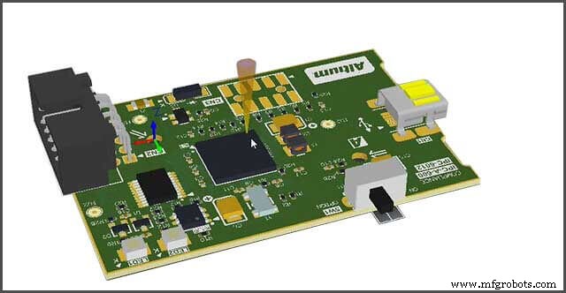
为您的设备成功开发印刷电路布局后,您需要接下来制作电路板。在开始制造之前,看看最终产品的外观总是一个好主意。某些软件(如 Proteus 或 Altium)具有 3D 布局查看器,可以让您以 3D 方式查看电路板以感受电路板的外观。
在发送您的设计进行制造之前,您首先需要生成制造商将使用的文件格式并决定使用什么。 WellPCB 是制造业的领导者。
印刷电路板和 PCB 制造工作的最佳选择。
PCB 设计必须转换为大多数专业人员使用的 Gerber 文件,这是 PCB 行业的标准。 Gerber 文件包含在 PCB 生产中使用的所有必要设计文件。 WellPCB 接受四种文件格式(Gerber、pcb、pcbdoc 或 cam 文件格式)。
WellPCB 在两面都打印丝网印刷,而且不收取任何额外费用。在印刷的丝网印刷层上包含零件编号会很有帮助。了解董事会规范也是一个好主意。 WellPCB 的线/轨道宽度和空间至少为 3mil。确保您的设计不超过此值。使用您的软件设计规则检查以确保您的电路板不超过制造商的生产能力。
丝印要求说明了 PCB 上所需的颜色,并且大多数是 UV 固化油墨并且符合 RoHS 标准。
1. 白色
2. 黄色
3.黑色
这些是使用最广泛的颜色;也可以使用其他颜色,颜色会增加处理时间和成本。
要在 WellPCB 上订购您的 PCB,请按照以下简单步骤操作:
4. 访问 WellPCB PCB 在线报价部分 – https://www.wellpcb.com/pcb-quote
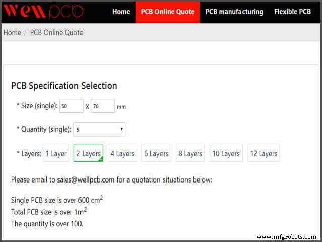
5. 填写您的板子详细信息,然后单击添加到购物车。需要了解有关在线订购定制 PCB 电路板的信息。对于您需要的 PCB 板,您可以通过 WellPCB 联系我们,最少数量为 5 块面包板 PCB
6. 注册一个新账号。
7. 上传您的 PCB Gerber 或。 Brd 文件。
8.订购您的物品并等待它交付。
WellPCB 还有助于对所有客户的文件执行完整的 DRC 检查,这很有帮助,尤其是在设计存在一些问题或错误的情况下。用户将收到问题提醒,避免在电路板制作过程中浪费时间和金钱。
现在您坐下来等待您的印刷电路板到达。其 PCB 服务的 PCB 制造交货时间至少为 24 小时,对于 8 – 12 层 PCB 的最短时间约为 120 小时。
下一章,我们将讨论一些PCB术语和WELLPCB能力。
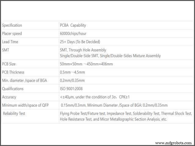
WellPCB PCB 功能和一些常见的 PCB 术语
WellPCB 是印刷电路板的领先制造商,并提供印刷电路板组装以配合其 PCB 原型。
这使 WellPCB 成为您整个产品开发的首选制造商。此外,他们还为您的电子板外包组件提供交钥匙服务。面包板PCB
WellPCB is focused on offering PCB prototypes services and not just large-scale manufacturing. Their PCB prototypes services go at a minimum of 5 units. Not only are they offering prototyping services but also packaged at some meager prices.
A promotional price of $3.99 for users looking for 1-2 layers, 10pcs PCB prototypes, and a board of less than 10cm*10cm.
WELLPCB is capable of producing 100,000 square feet of 2-32-layer PCBs and delivering over 5000 varieties monthly.
With a quick turn to meet 24-hour delivery for double-sided PCBs, 48-hour for 4 to 8 layers, and 120-hour for ten layers or higher PCBs. Their standard lead time is about 5 – 6 days and an Expedited time of 24 – 48 hours.
4.1 The following are WellPCB PCB manufacturing capabilities
1. Support Material:FR4, High TG FR4, Halogen Free material, CEM-3, Rogers HF material.
2. Layer counts 1-32 layers.
3. Finished Copper Thickness:0.5-5 oz.
4. Finished Board Thickness:0.2-6.0mm.
5. Min. Line/Track Width:4mil.
6. Min. Line/Track Space:4mil.
7. Min. Contour Tolerance:+/-0.1mm.
8. Min. Finished Diameter of PTH Hole:0.1mm.
9. Max. Board Thickness/Hole Ratio:12:1.
10. Min. Solder Mask Bridge:4mil (Min. SMT Pad Space 8mil).
11. Min. Legend(Silkscreen) Track Width:5mil.
12. Solder mask color:green, black, blue, white, yellow, matt, etc.
13. Solder mask hardness:6H.
14. Legend/Silkscreen Color:white, yellow, black, etc.
15. Surface Treatment:HAL, Lead-Free HAL, Immersion gold, OSP, Immersion Tin, Immersion silver, etc.
16. Other Technology:Gold finger, peelable mask, Non-across blinded vias, characteristic impedance control, Rigid-flex board, etc.
17. Reliability Test:flying probe test/fixture test, impedance test, solderability test, thermal shock test, hole resistance test.
18. Flammability:94V-0.
4.2 Breadboard PCB —Surface Finish
A PCB surface finish is a coating between a component and a bare board PCB. It is applied for two primary reasons:to ensure solderability and to protect the exposed copper circuitry.
Standard surface finishes preference – Non-RoHS or RoHS compliant.
1. HASL (Hot Air Solder Level) – Contains Lead non-RoHS, cheaper and quite popular.
2. ENIG (Electroless Nickel Immersion Gold) – Most popular finish and lead-free, but expensive
3. Immersion Silver – RoHS compliant will tarnish like any silver product
4. OSP – Organic Solderability Preservative
5. LF-HASL (Lead-Free Hot Air Solder Level)
6. Immersion Tin – Used the least of all finishes
4.3 Soldermask
Soldermask is the color to be used for the PCB prototypes finish. Any color can be used. However, sticking to standard colors is the best and more professional. The most popular are:
1. Green
2. Blue
3. Black
4. Red
5. White
6. Yellow
Mask can be in either Matte or Gloss in those above colors. Matte is less readily available due to Gloss is most widely used. Processing Matte for specific colors may add time due to equipment change and processing cleans up and application.
4.4 Breadboard PCB —Silkscreen
Silkscreen is the printing done on the PCB for identification. It is used on the component side to identify components, test points, PCBA part numbers, warning symbols, company logos, and manufacturer names. The following are some of the colors being used:
1. Black
2. White
3. Yellow
Those are the most widely used colors; others are available; however, colors can add to process time and cost like MASK. Ask if you have special requirements for your product.
In the next chapter, we will talk about how to move your PCBA mode.
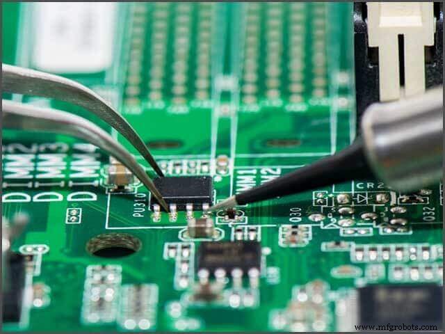
Breadboard PCB–Moving from PCB Prototypes to PCBA
So, what’s PCB Rapid Prototyping. PCB assembly. Directly speaking, PCB Rapid Prototyping. PCB assembly. Directly speaking, PCB Rapid Prototyping. 3D PCB Printing makes the PCB and does the Printed Circuit Board Assembly (PCBA, an abbreviation for printed circuit board assembly, which refers to the combination of PCB prototypes manufacture, components sourcing, and B3D PCB Printing makes the PCB and does the Printed Circuit Board Assembly PCBA is the PCB with components assembled).
So now you have your printed circuit board available and ready to populate the board with the needed components. You might be tempted to solder this manually yourself. This might be a good option, especially when the number of panels is less than five or, worst case, ten units; anything more than that might not be a good idea but going the route of PCB Rapid Prototyping. 3D PCB Printing not only makes the PCB but also does the Printed Circuit Board Assembly PCBA.
5.1 Breadboard PCB —Assembly Types of PCBA
The main assembly types of PCBA are shown below:
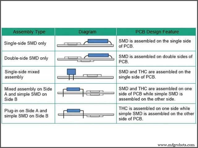
Those are the commonly used PCB Rapid Prototyping. 3D PCB Printing makes the PCB and does the Printed Circuit Board Assembly (PCBA assembly types. SMD means Surface Mount Devices, and THC implies Through Hole Components).
PCBA helps engineers, product developers, hobbyist and others to self-populate the board with needed components by a manufacturing firm.
It is usually faster and cheaper on bulk orders. Getting started with PCB Rapid Prototyping. 3D PCB Printing makes the PCB, and does the Printed Circuit Board Assembly (PCBA is also relatively simple as far you have the necessary resources).
Just like, WellPCB is capable of handling all your possible PCB prototypes works, they also offer an accompanying production film work that you require to manufacture PCBs. In the case of PCBA service to help one streamline the whole board development process. It does not cost much more to have the PCB populated unless you tack on additional steps in the process, such as burning a program to the MCU or running 100% test on the finished boards.
To get started with PCBA, you need to have all the required documents.
Aside from your PCB prototypes design file, you will need a design specification if there are special needs for your work, a bill of the material (BoM) list for the number of components on your board and also can be generated from the software being used, and part placements made from the software used.
When starting your PCB Assembly, one crucial take note is the sourcing of the components for the board.
The board owner can decide to source for the parts alone and send them to WELLPCB for assembly or let WellPCB handle the integral components sourcing, which I feel is better. Of course, partial supply can also be agreed upon.
Go to PCB Assembly on WellPCB here and fill the Request for Quotation (RFQ) form. Input as many details as possible and send it. WellPCB will get in touch if they need more information from you and continue the assembly process order.
The WellPCB Bill Of Materials (BOM) of a PCB gets fitted onto aboard. PCB Assembly process can take up to around 25 days for large volume manufacturing, which is an excellent time for large volume PCB assembly compared to other PCB Assembly manufacturers. This will make it easy for a pick and place machine to easily pick and place the components on the PCB Assembly capabilities:
More information about WellPCB SMT). This will make it easy for a pick and place machine to easily pick and place the components on the PCB Assembly capability can be found here.
At this point, all you have to do is to sit down and wait for your populated PCB to be available and sent to you. This concludes the end of this chapter, and the next chapter will discuss how to save money when doing PCB and PCBA.
Saving Money in PCB Prototypes and PCBA Manufacturing
Now congratulation, you have your fully developed hardware PCB prototypes or, better still, hardware board. For newbies, this will have been a good experience, and also a lot of money must have been sent which could have been avoided.
Some of the money spent could have been avoided due to unnecessary complexity and errors in the PCB and circuit design.
This chapter will show some of the handy tips and tricks that can help you save even millions when doing large volume manufacturing.
6.1 Breadboard PCB —Keep Your Board Size at a Minimum
Keeping your board size at a minimum is crucial in saving costs and making your final product as portable as possible. The bigger it gets, so do the prices. If the board becomes smaller, so does the cost.
Also, making your board too small might not save you cost since assembling and preparing your board might require specialized equipment.
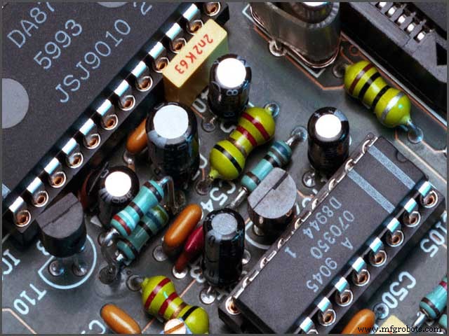
6.2 Using Surface Mount Components as Much as Possible
You might be tempted to use DIP (dual in-line) package, commonly known as Through-hole components, because it’s possible to easy to use but might not be the best cost-saving option.
1. Using surface mount components will reduce the number of holes that need to be drilled on your board typically used for through-hole parts.
2. Using surface mount components will also reduce the board size.
3. Using surface mount components will make the board assembly faster and lesser equipment used.
6.3 Set Your Design Up for Penalization
By going on board penalization, you can save yourself a ton of money. Getting all of your boards on one panel means that a rapid-fire pick and place machine can get all your parts placed in one go without requiring any additional setup time.
6.4 Silk Screening Help You Reduce Your PCB prototypes Costs?
Requesting silk screening on one side will cut your artwork costs in half. Sticking with standard colors and larger geometries will also prove beneficial. Understanding these constraints can help you to better PCB prototypes pricing and cost savings.
6.5 Breadboard PCB —Use the Right Via for the Job
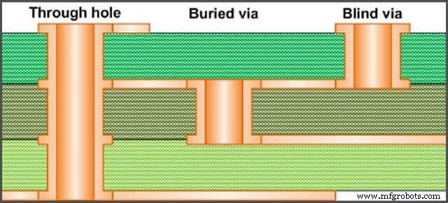
There are three types of vias – through-hole vias, blind vias, and buried vias. The last two are only going to be used for high-density and high-frequency PCBs. So, this one is simple, if your design doesn’t need these types of vias, leave them out to avoid any extra manufacturing costs.
This concludes the end of this chapter and the end of this guide. Using standard materials and several of these tips mentioned above can save you several thousand to millions of dollars when embarking on large volume manufacturing.
Breadboard PCB–Conclusion
When building and launching your products to market, some other things also need to be considered.
1. Certifications – Every wireless-based product needs to go through some certification process to be clear of any hazards or issues and be permitted to the market.
2. Enclosure – Depending on the type of product you are building, you might need some enclosure around your board to give it some artistic look or for some reason.
3. Quality Control – Quality control issues a formal inspection report for review and shipment approval. You should expect each shipment to be inspected and approved before being released. Such a protocol creates a closed-loop process that builds in continuous improvement for consecutive production runs.
This guide should give you enough head start in launching your following product. Taking an idea from concept to production is not for the faint of heart.
You have to withstand failures, criticism, mishaps, and managing the whole manufacture process can be very challenging. Still, a manufacturer like WellPCB is in the business to help you succeed. Breadboard PCB
工业技术