

印刷电路板设计指南
印刷电路板,也称为 PCB,是当今每个电子部件的核心。这些小型绿色组件对于日常电器和工业机器等都是必不可少的。 PCB设计和布局是任何产品功能的重要组成部分——这决定了一件设备的成败。随着技术的不断发展,这些设计也在不断进步。如今,由于电气工程师的创新,这些设计的复杂性和期望达到了新的高度。
PCB 设计系统和技术的最新进展对整个行业产生了广泛影响。因此,PCB 设计规则和生产流程已经发展,以实现新的布局和功能。今天,更小的轨道和多层板在大批量生产的 PCB 中很常见——这样的设计在几年前是闻所未闻的。 PCB 设计软件也有助于这一进程。这些程序提供了工具,电子工程师可以利用这些工具从头开始设计更好的 PCB。

即使有了这些改进的功能,PCB 板布局也很难设计。即使是最有经验的电子工程师也可能难以在 PCB 上创建电路或如何根据行业最佳实践设计 PCB 板。更困难的是创建一个高质量的板来满足客户的需求。对于客户设计,平衡 PCB 的功能与最佳设计实践是一个复杂的过程。这就是为什么我们概述了设计 PCB 的过程,包括一些基本的 PCB 设计规则。
确定需求
主要的 PCB 设计步骤中的第一个是需要的。对于大多数电子工程师来说,这些要求是由客户规定的,客户将列出 PCB 必须满足的所有要求。然后,电子工程师必须将客户列出的需求转换为电子形式。从本质上讲,这意味着将它们翻译成一种电子逻辑语言,这是工程师在设计 PCB 时将使用的语言。

项目的需要决定了PCB设计的几个方面。这包括从材料到 PCB 本身的最终外观的所有内容。 PCB的应用,例如医疗或汽车,往往会决定PCB中的材料。例如,许多用于电子植入物的医用 PCB 都是用柔性底座制成的。这使它们能够适应狭小的空间,同时还能承受内部有机环境。 PCB 的最终外观主要取决于其电路和功能——例如,许多更复杂的 PCB 由多层制成。
电子工程师将确定并列出这些需求,然后使用此需求列表来设计 PCB 的初始原理图以及 BOM。
原理图
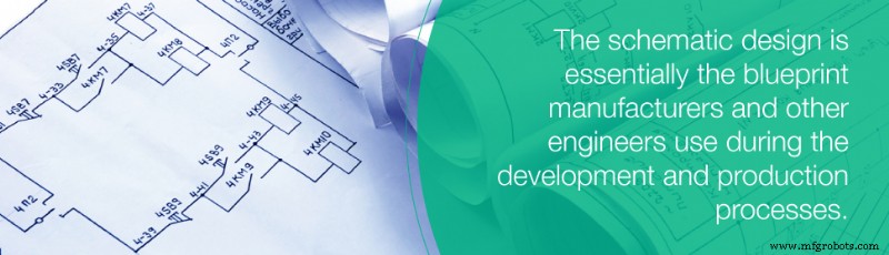
原理图设计本质上是制造商和其他工程师在开发和生产过程中使用的蓝图。原理图决定了PCB的功能、设计的特点和元件的放置。 PCB的硬件也在这个示意图中列出。该设备包括PCB的材料、设计中涉及的组件以及制造商在生产过程中需要的任何其他材料。
所有这些信息都包含在初始设计阶段的原理图中。完成第一个原理图后,设计人员进行初步分析,检查潜在问题并根据需要进行编辑。然后将原理图上传到用于 PCB 设计软件的特殊工具,该软件可以运行仿真以确保功能。这些仿真使工程师能够捕捉他们在初始原理图检查期间可能遗漏的任何设计错误。之后,可以将电路的电子设计转换为“网表”,其中列出了有关组件互连性的信息。
在考虑他们的原理图设计时,电子工程师应该从一开始就牢记一些关键的电路板设计基础。在原理图开发阶段要实施的一些考虑因素包括:
-

- • 选择合适的 PCB 面板尺寸:选择与要使用的设备最兼容的电路板尺寸是基本但经常被遗忘的最佳实践。这样,就不会浪费额外的空间,将走线保持在最小长度,并且总体材料成本保持在较低水平。然而,重要的是要确保设计规范针对大规模生产进行了优化。电路板设计太小可能不适合批量生产设置,因为这些设置会在部件之间产生足够的差异以破坏较小的设计。
- • 选择正确的网格:始终设置并应用网格间距以适合大多数组件。坚持这个网格是工程师可以做的最有益的事情之一,以避免间距问题,因此选择最适合工作的网格是至关重要的。如果某些部分不能很好地与网格一起使用,设计师应该尝试寻找替代品,或者更好的是,使用自行设计的产品。
- • 尽可能多地实施 DRC:许多 PCB 组装公司都犯了一个错误,即仅在设计流程结束时才运行设计规则检查 (DRC) 软件。这会让小错误和有问题的设计选择累积起来,从而在设计过程结束时进行更多的补救工作。相反,设计师应该尽可能多地使用 DRC 检查他们的工作。这使他们能够尽快解决 DRC 发现的问题,并在设计过程结束时最大限度地减少大规模更改的数量。这最终节省了时间并简化了编辑过程,因此不会那么繁重。
材料清单

在生成原理图的同时,电子工程师还开发了精美的材料清单或 BOM。这是 PCB 板原理图中使用的组件列表。一旦 BOM 和原理图都完成,电子工程师将两者都交给布局工程师和组件工程师。这些工程师检查细节并获得项目的必要组件。具体来说,组件工程师负责选择在最大工作电压和电流方面符合原理图的组件。他们还负责选择符合合理成本和尺寸参数的设备。
BOM 组件必须满足的五个最重要的方面包括:
- • 数量:采购的组件数量必须至少满足 BOM 中列出的组件数量。
- • 参考标号:必须根据其在 PCB 电路中的位置来识别每个组件。
- • 价值:每个组件都应在特定的值范围内,包括欧姆、法拉等。如果客户关心成本,则成本是一个因素。
- • 占地面积:必须列出每个组件的位置。
- • 制造商部件号:跟踪部件号以防出现故障,以供组装商和制造商参考。
除了这些基本的 BOM 指南之外,在制定 BOM 和一般原理图时,最好记住一些注意事项。其中包括以下 PCB 设计技巧:
- • 集成组件:选择组件是设计师最重要的工作之一。为了帮助完成该过程,您可以选择选择具有高或低组件值和类似效果的分立组件。通过集成这些组件并生成一个小的标准值类别,您可以有效地简化物料清单并降低产品成本。
-
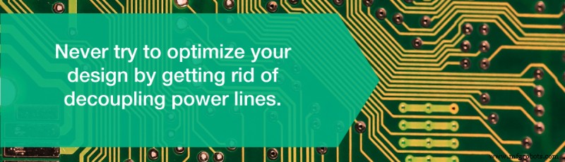
- • 应用去耦电容:切勿试图通过去掉去耦电源线来优化您的设计。许多设计人员在错误地尝试降低成本时避免使用这些电容器。电容器价格低廉且非常耐用,可延长您的设计寿命。电容器还有助于保持电路板的有序性,同时保持低成本。如果您担心自己的 BOM,请关注上述提示。
PCB 元件放置
每个组件都应在电路板设计上具有指定的位置。选择正确的位置是棘手的部分。确定元件的最佳位置取决于设计师的许多因素和考虑因素,包括热管理、电气噪声考虑和整体 PCB 功能。然而,在大多数情况下,设计师会按以下顺序放置组件:
- • 连接器
- • 电源电路
- • 敏感和精密电路
- • 关键电路组件
- • 所有其他元素
在设计周期的这个阶段需要牢记的更多设计注意事项包括:
- • 识别和划分有关组件和所需测试点:如果 PCB 上有任何令人担忧的组件,请将其放置在所需测试点附近,以便更及时地检测故障。
- • 灵活应用丝网印刷:丝网印刷可以标记范围广泛的信息,供 PCB 制造商、工程师、组装人员和测试人员在 PCB 组装过程的各个部分使用。在丝印上,标记功能、测试标记以及元件和连接放置方向是个好主意。尽量在印刷电路板的顶部和底部都进行丝印,避免重复工作,同时也为手工组装人员明确了方向,简化了生产过程。
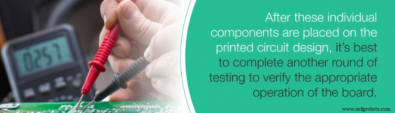
在将这些单独的组件放置在印刷电路设计上之后,最好完成另一轮测试,以验证电路板的适当操作。这将有助于识别任何有问题的设计选择并帮助识别任何潜在的调整。
路由
一旦将组件放置在 PCB 上,PCB 设计基础的下一步就是将它们全部连接起来。板上的每个元件都是通过走线连接的,走线是通过适当的布线实现的。然而,由于设计人员必须考虑许多因素,布线需要自己的设计过程。这些因素包括功率水平、信号噪声灵敏度、信号噪声产生和路由能力。
幸运的是,大多数 PCB 设计软件将使用从原理图开发的网表来布线。该程序通过使用可用于连接的层数并计算最佳路线以利用空间来做到这一点。该程序还可以根据需要更改设计。这可能需要大量的计算能力,尤其是对于较大的模型。结果是更长的布线过程 - 当组件放置在特别密集的排列中时,程序可能会花费更多时间。
虽然大多数 PCB 软件会根据原理图的网表进行走线布线,但该软件并不通用。并非所有 PCB 设计人员都使用自动布线软件,甚至那些确实倾向于仔细检查走线是否存在问题的设计人员。无论如何,这始终是一种很好的做法,因为即使是计算机也会产生设计师不喜欢的结果。
走线的一般经验法则是,宽度为 10 至 20 mil 的走线能够承载 10 至 20 mA 的电流。另一方面,宽度为 5 至 8 mil 的走线可承载低于 10 mA 的电流。对于大电流 PCB 设计或信号快速变化的 PCB 设计,这是一个特别重要的考虑因素,因为将它们路由到高频节点将需要特定的走线宽度。
-
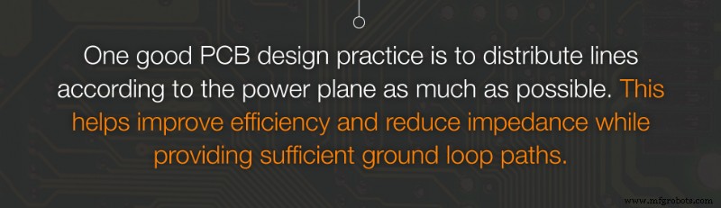
- • 适当分配电源线和接地线:大多数 PCB 设计人员会专门使用一个电路层作为接地层。另一个通常用作电源平面。 This helps reduce the level of noise in the PCB and enables the designer to create low source resistance connections. One good PCB design practice is to distribute lines according to the power plane as much as possible. This helps improve efficiency and reduce impedance while providing sufficient ground loop paths.
- • Maintain Short Traces:Make sure traces are as short as possible at every stage of the design. While most PCB assembly processes include a step for optimizing trace length, this should be practiced at every design stage. This rule should be even more closely observed when the designer is working with an analog or high-speed digital circuit. These types of printed circuits, commonly found in automobiles and telecommunications devices, are more severely impacted by impedance and parasitic effects.
Checks
Checking the design is possibly the most important step of the design process. This segment of the process considers everything about the design, looking for potential problems that plague PCB designs.
For example, a common problem in PCB designs is heat. PCB with a perfect thermal design can keep the entire board a consistent and uniform temperature, preventing heat spots. However, such heat spots and temperature inconsistencies can be caused by any number of design features, such as copper thickness variations, the number of layers in the PCB, larger PCB board sizes and the presence or absence of thermal paths.
A simple design check can catch potential problems in PCB heat management, most PCB DRC software can pick them up as well. There are several methods to reduce PCB operational temperatures, many of which are mitigated by PCB design basics. A few of these heat-managing tips include:
- • Connect solid ground or power planes with more layers directly to the heat source of the PCB. These planes are typically more able to dissipate heat, since they tend to contain more copper.
- • Establish effective heat and high-current routes to help direct and dissipate heat. This can help optimize heat transfer.
- • Maximize the area used for heat transfer. This can help maintain a lower temperature across the board. This is something that must be considered early in the design process, however, as it can impact the size of the board.
Most DRC software can catch the aforementioned problems. The DRC software takes all the details about a PCB design and determines whether the layout satisfies a list of predetermined parameters. These are called PCB design rules. Ideally, as previously mentioned, the DRC should be used throughout the design process to identify problem areas early on. However, if all else fails, using DRC after everything else is complete can save a lot of design time and confusion between the designer and the assembly company.
The check step of the design process doesn't just include the DRC check - it also includes several other physical verification processes, including a layout-versus-schematic (LVS) check, an XOR check, an electrical rule (ERC) check and antenna check. More advanced PCB manufacturers may use additional checks and rules to improve yield, but these are the basic checks designers and manufacturers typically use.
Furthermore, it's good practice to verify manufacturing parameters before submission. Before submitting the final design for production, the designer should personally generate and verify the PCB manufacturing parameters. Though most manufacturers are willing to download and verify design files for their client, it's better to double-check the design before sending it in. This can help avoid any confusion or misunderstanding and can avoid losses due to manufacturing with incorrect parameters. This verification step can also expedite the process by decreasing the amount of time needed to correct and reverify the design before manufacturing starts.
Find an Assembly Service for Your Design
PCB design can be simplified by implementing the above basic techniques and best practices. It can be made even simpler by partnering with a PCB supply and assembly service that works with you to make the best, most cost-effective PCBs possible.
PCBCart is a worldwide printed circuit board supplier, with loyal customers around the globe. We know you can't afford to use poor-quality PCBs, which is why we follow the most demanding international quality standards. We also know you need cost-effective materials, which is why we offer PCBs at unbeatable prices. We offer you the best PCB services at the lowest price possible to allow you to focus less on supplier and more on your business.
Our expert customer-service representatives are waiting to help you. Contact us today to learn more about PCB design rules and assembly processes and how we can help you with your next PCB design project. If you already have a design and want to get started on assembly, feel free to get a quote by clicking below buttons:
Helpful resources:
• PCB Design File Requirements for Quick PCB Assembly Quote and Production
• Full Feature PCB Fabrication Service Starting from 1 Piece
• Advanced Turnkey PCB Assembly Service - Multiple Value-added Options
• PCB Design Tips to Better Take Advantage of PCBCart's Assembly Capabilities And Save Cost
• Design PCBs to Better Take Advantage of PCBCart's Manufacturing Capabilities
工业技术