

多层池 - 最全面的引导您了解 PCB 层
在多层池上,印刷电路板具有各种不同的层。这些层次可能会使那些对利基市场不完全敏锐和精明的人感到困惑。
大多数快速制作的 PCB 原型有 2 层。然而,许多电子设备并不局限于双层板。他们需要更高更细的木板。
本文将帮助您更好地了解 PCB 层及其工作原理。
什么是 PCB 层
1.1 PCB 层定义
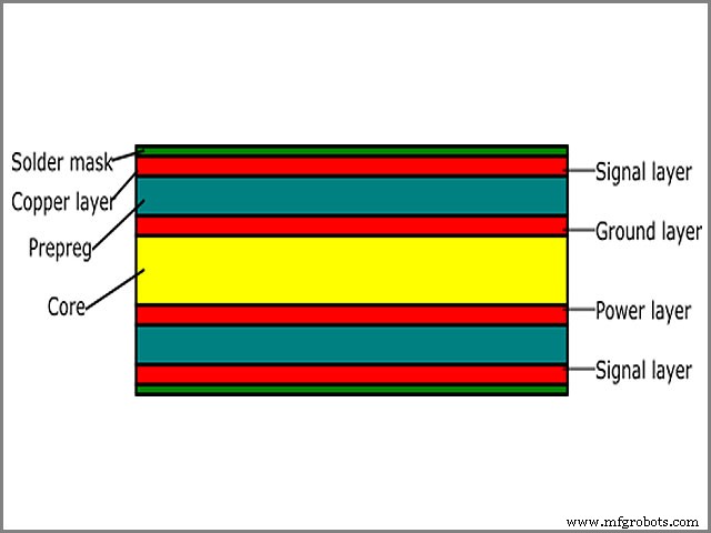
印刷电路板根据要传递的信息具有不同的含义。关于PCB层,也描述为按一定数量和顺序给出的铜层。
铜层可以称为信号层或仅称为层。 PCB 层是根据它们的定位和它们提供的功能来命名的。 PCB按铜层数排名。
例如,具有一层或两层的电路板可以分别称为 1 层 PCB 或单面 PCB 和 2 面层 PCB 或简称为双面 PCB。
PCB Layers有多种类型,常见的有以下几种:
1.机械层
2. 覆盖层/丝印层
3. 路由层
4. 阻焊层
5. 焊膏层
6. 隔离层
7. 接地层和电源层
8. 分割平面
请记住,并非每个 PCB 都由上面列举的所有层组成。您的设计细节决定了对各种层类型的需求。单层板通常由六层组成。
其中包括机械层、阻挡层、布线层、覆盖层、阻焊层以及焊膏层。
对于多层 PCB,它们由六层组成,外加其他电源、接地层和附加布线层的组合。
两层、四层、六层PCB是最常见的电路板,12层以上的PCB也不少见。
1.2 机械层
虽然您可能有多个机械层,但您仍然需要一个 - 至少 - 来构建您的电路板。最基本的机械层定义了电路板的物理尺寸。
机械层也称为机械层 1。制造商将用于从其材料中切割出电路板的层。
印刷电路板可以简单到只有一个布线层,概述了电路板的物理尺寸,也可以复杂到包含许多层的电路板,包括本文中提到的所有层。
另一方面,当单独考虑时,每一层都具有特定且仅具有的功能。了解每一层的用途至关重要,因为一旦您这样做,无论电路板多么复杂,PCB 的构建都会变得非常简单。
该框架可以是简单的矩形,也可以是具有弯曲角加/或切口的复杂形状。
尽管这种情况很少见,但仍包含更多机械层,指定工具规格和其他杂项自动信息。然而,大多数印刷电路板不需要这些额外的机械层。
层堆叠(与 PCB 层区分)
2.1 什么是层堆叠?
层堆叠是一种层的正确放置。 PCB一般分为三类:
- 单层。
- 双层。
- 多层。
上述术语描述了 PCB 中铜层的数量。多层PCB描述的是4层、6层、8层范围内两层以上的PCB。
在多层中,顶层和底层称为外层,而中间层称为内层。与双层和单层 PCB 相比,多层 PCB 制造的复杂性使其成本相当高。
在层堆叠中,您可以考虑一些事项,其中包括:
- 基材。
- PCB 层顺序。
- 铜的厚度。
不同的电路设计具有适合它们的不同层堆叠。层堆叠对于印刷电路板的功能至关重要。
当层堆叠没有很好地规划时,可能会出现不同的问题,其中包括:
- 信号串扰。
- 联轴器。
- 过冲。
- 下冲。
- 电磁干扰。
- 信号耗散。
为避免上述问题甚至更多问题,精心规划的 PCB 层堆叠至关重要。您可以通过设计高效的 PCB 层堆叠来节省大量成本,这可以大大防止由于设计不当而可能出现的问题。
在层堆叠中,除了 PCB 层顺序之外,还考虑了基板材料、铜厚度。
不同类型的电路设计有不同的层堆栈。精心规划的 PCB 层堆叠可确保 PCB 的最佳性能,例如减少电磁干扰、信号串扰、耦合、过冲和下冲以及信号耗散。
待完成的设计和一次合格的设计可以显着降低成本和设计周期时间。如果信号完整性问题在它们出现之前被消除是可能的。
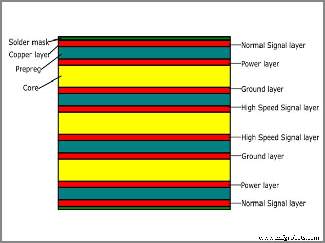
图 1 下面是两个 8 层的堆叠方案,强调层的变化顺序。
除了信号层,电源层在成功的产品开发中也起着至关重要的作用。
信号,无论是数字信号还是模拟信号,都可以通过微带线或带状线进行路由,从而减少串扰,从而提高信号完整性。
低频信号走内层,高频信号走外层。
最好在每个信号层附近放置一个接地层;然而,为了减少层堆叠和制造成本,接地层放置在每两个信号层之后。电源层也应与实现紧密耦合的接地层相邻。
在多个电源轨的情况下,电源平面被分成多个部分。通常,PCB厚度为1.6mm,但要保持1.6mm的厚度超过12层是有挑战性的。
在图1下面的两个8层中,显示了堆叠方案,强调了层的变化顺序。
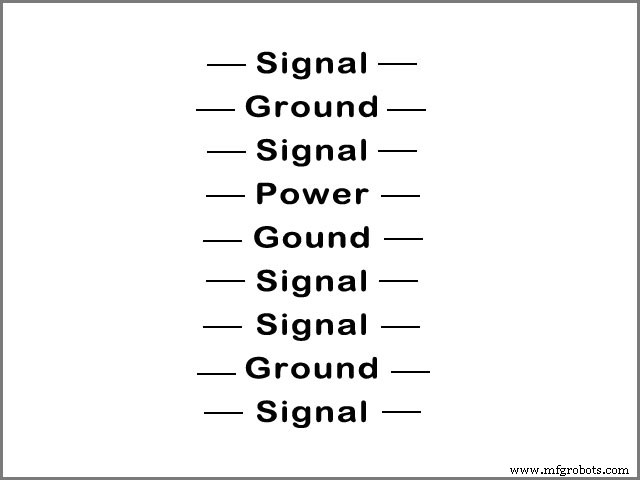
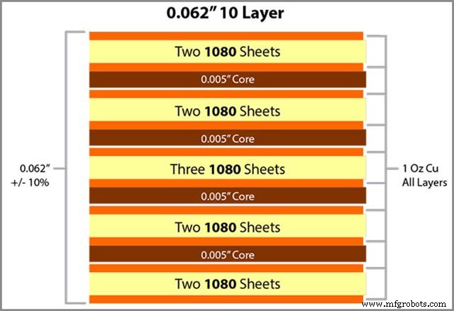
图2描述了10层PCB Stackup方案。
2.2 区分 PCB 层与层堆叠
尽管这两个术语似乎意味着同一件事,但事实并非如此。如上所述,层堆叠是一种层的正确放置。
另一方面,PCB层是指按一定数量和顺序给出的铜层。层堆叠与层的规划有关,而PCB层与层的数量和顺序有关。
PCB 层类型
3.1 1层PCB
通常称为单层PCB,一层PCB是从一侧印刷的;这意味着PCB板的一侧与导电材料一起,而另一侧则连接电子元件。
起初,所有的 PCB 都是手动设计的,但由于技术进步,现在可以使用专用软件(如 eagle PCB 软件)来创建它们。它是通过使用具有此程序的计算机来完成的。
单层 PCB 有不同的类型。其中一些包括以下内容:
• 柔性PCB。这些单层 PCB 由柔性材料而不是刚性材料制成。在这种情况下可以使用的材料包括塑料。这种单层PCB的生产成本相当高,不经济。
• 刚性PCB。这些单层 PCB 由玻璃纤维等刚性材料制成。它们不灵活,因此不允许电路弯曲。它们通常用于大多数设备,例如计算器、电源等。
• 高频PCB。这些单层 PCB 用于需要很高频率才能工作的电路中。在为此类 PCB 选择合适的材料时,热膨胀、吸水性和介电损耗是考虑的一些因素
• 刚柔结合PCB。这些单层 PCB 由塑料和玻璃纤维组合而成。这两种材料都组合成一个单层。这种组合因此减小了 PCB 的尺寸和重量。
• 铝背板PCB。这些单层 PCB 由铝材料制成。这块PCB的设计和铜的差不多,只是在使用过的文章中有所不同。
如您所见,层 PCB 非常简单。但是,不要让他们的简单性欺骗您他们可以实现的目标。它们可能很简单,但它们对在复杂设备中工作产生了很多影响。它们执行一些功能,其中一些包括以下内容:
- 1.它们用于无线电和立体声设备电路。
- 2.它们用于数码相机。
- 3.它们用于复印机和打印机。
- 4.它们用于数字计算器。
- 5.它们用于自动售货机。
单层PCB有一些优点,例如:
- 易于构思和设计。
- 易于安装。
- 性价比高。
- 这很容易理解。
- 发生短路的可能性很小。
- 更可靠、更高效。
3.2 2 层 PCB
两层PCB也称为双层或双面PCB。它主要由FR-4玻璃环氧树脂基板层压薄铜膜或两面层制成。它是设计最简单、最经济的PCB。
两层 PCB 可以很容易地由专业的 PCB 原型制造工厂(例如 wellpcb.com)制造并在家中制造。两层PCB只有顶层和底层铜层。
这是一个简单的设计,别忘了它也很经济。这种 PCB 设计可以在家里使用正确的软件轻松制造。它大多只是由 PCB 原型公司制造。
本设计中的PCB层主要是构成顶层的信号层,底层由电气元件组成。双层PCB的所有元件如下:
- 追踪。
- 垫。
- PCB 层,包括丝层、顶层和底层。
- 阻焊层。
有些地方使用了双层PCB。一些应用领域包括:
• 在照明中。双层PCB用于LED灯,因此它们具有功率。
• 在医疗设备中。双层PCB用于心脏起搏器和CAT检查机等医疗设备。
• 汽车和航空航天工业。在汽车行业和航空行业中,PCB 都得到了广泛的应用。更准确地说,双面PCB主要用于这两个行业。
双层PCB具有广泛的优势。您可以在下面查看其中的一些:
- 它们使铺设轨道更简单。
- 允许分段增加厚度。
- 提供扩展的温暖散射。
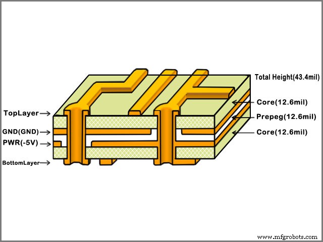
3.3 4层PCB
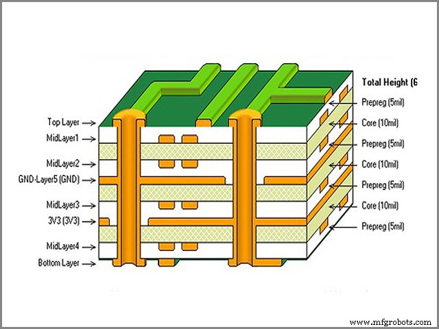
四层 PCB 有四个铜层。顶层和底层是布线层,而夹在中间的两层是电源层和接地层。
四层PCB铜层之间是Core和Prepreg。在制造过程中,所有这些元件在高温高压下通过层压板结合在一起(夹在中间),以确保整个叠层保持在一起。
四层PCB可以包含通孔、盲孔和埋孔。对于四层PCB,埋孔只能在第二层和第三层之间,盲孔可以在顶层(第一层)和第二层之间或底层(第四层)和第三层之间。
四层板的典型叠层是内两层的电源和接地,然后是外两层的信号。通常将两个信号层垂直布线。
各层是否由电源和接地分开并不那么重要,但如果相邻层上有信号,则将串扰降至最低就变得更加重要。
至于编号,通常从 1 到 n,从上到下。这是唯一的约定;您可以随心所欲,因为您将在发送文件进行生产时提供堆叠信息。
在制造四层 PCB 时,如果您有制造工厂,成本可能会非常有用。
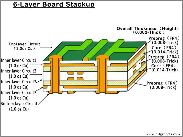
3.4 6层PCB
使六层PCB的设计免疫且安静。与其他 PCB 相比,六层 PCB 具有优势是有一些原因的。一些想法包括以下内容:
• 第三层和第一层之间的跟踪不需要任何特殊处理。
• 每条走线都靠近地面。
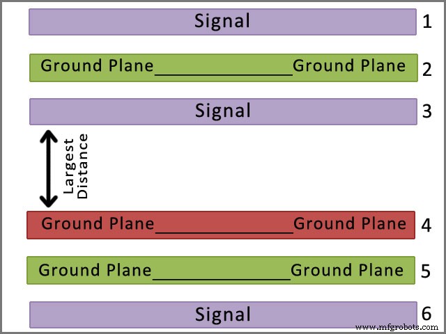
3.4.1 参考平面
参考平面用于传输返回电流。四层设计中,第一层在第二层有高频回币,第四层在第三层也有高频;因此与六层PCB没有区别。
当参考平面靠近布线层或信号层时,您将切掉决定辐射发射的环路区域 以及高频时的敏感性。
以下是使六层堆栈运行良好的一些因素。
1.每条走线与地面的距离。
2. 接地层和产生规划电容的电源接近。
3.第三层和第一层之间的跟踪,不需要任何特殊处理。
4. 第四层参考平面高于第二层的距离。
3.4.2 常见的 6 层 PCB 叠层设计
最好的六层 PCB 设计需要缝合以连接 PCB 中的两个接地层,它们应该将电流返回到参考层。有人说增加额外的接地层有助于屏蔽辐射和抗扰度。
3.4.3 PCB 平面切割杀死 EMC
平面切割可能在排放和敏感性方面对 EMC 造成毁灭性影响。平面切割或空洞是指电源或接地平面无意或有意切割平面的给定部分。平面切割有不同的尺寸和形状。
平面上的电流返回路径在几千英寸之外,在良好的设计中,走线靠近平面,因此使返回电流路径靠近,从而形成相对较小的环路面积。
当您在铜平面层中引入一些空隙时,您必须创建一个循环,以便在空隙和平面切口上运行走线。它使当前的循环区域更加重要。
3.5 8层PCB
一块八层板可以多增加两层布线,或者通过多增加两层来提高 EMC 性能。
八层板相对于六层板的成本增加百分比低于从四层到六层的百分比增加,因此更容易证明成本增加是为了提高 EMC 性能。
因此,大多数八层板由四个布线层和四个平面组成。
一般来说,要制作八层 PCB,需要交替使用铜层、预浸料和核心层。预浸料起到胶水的作用,将八层 PCB 叠层牢固地结合到一块板上。
按照提高电磁兼容性的规则,一个简单的八层 PCB 配置如下所示。需要注意的是,八层 PCB可以实现高信号完整性 与6层及以下PCB相比。
可以根据信号网络数量、器件密度、PIN密度、信号频率、板子尺寸选择PCB叠层设计方式。信号网络数量越多,设备密度越高; PIN密度越高,信号越高。
此外,为了获得良好的 EMI 性能,最好确保每个信号层都有其参考。
使用八层 PCB 具有一些优势。一些优点和好处包括:
• 减少可能导致中断的电磁干扰。
• 提高信号完整性。
3.6 多层PCB
3.6.1 32层PCB
它只是一个由 32 层组成的多层 PCB。将这些层放在一起作为单个 PCB 工作。这些PCB层是先进的,因此需要拿出技巧和精度。
PCB的每一个设计都从软件开始。对于 32 层的 PCB,制作了一个叠层,其中包含许多 PCB 层。这是通过使用将各层夹在一起的机器实现的。
选择使用 32 层 PCB 有一些原因。一些想法包括以下内容:
• 用于航空航天系统。
• 用于汽车领域。
32 层 PCB 背后的技术
为了制造 32 层 PCB,需要构建由多个 PCB 层组成的 Stack-Up。
在每两个双层 PCB 之间的绝缘纤维环氧树脂层的帮助下,将各种双层 PCB 夹在中间是可能的。这种绝缘材料也称为预浸料。
这意味着任何多层PCB的基本构建块都是双层PCB。
有了这种双面 PCB 制造技术,以及更先进的机器来处理日益增加的复杂性,32 层甚至 50 层 PCB 的制造是可以很好地实现的。
32 层 PCB 应用
为什么我们需要这些 32 层或 50 层 PCB?显而易见的原因之一是将所有必要的系统电子设备高效地嵌入到一块小型 PCB 中。
即使组件组装专用于顶层和底层,也可以在 Stack-up 之间放置组件。航空航天业在制作这些复杂的 PCB 设计方面做得非常出色。
在任何航空航天系统中,目标是尽可能少或没有电磁辐射。在设计阶段组织 PCB 可以很好地阻止这些排放。
每个 PCB 层通常专用于特定功能,与其他层不冲突。例如,中间层可以用作电源平面,而顶层和底层则用于放置元件。
3.6.2 多层PCB
多层 PCB 具有无限数量的导电层。然后在绝缘层的帮助下将这些层分开。它们通常组成在双面板的内侧。外层一般由单面板组成。
多层 PCB 的制造商利用热量和压力将每个 PCB 层粘合以形成一个 PCB 板。任何超过两层的PCB都可以归类为多层PCB。
Its stack-up must be made as that the complete board shall meet the electrical signal and power needs and meet the mechanical strength requirements. Most professional PCB designs can exhibit around 15dB fewer emissions.
There are some reasons why you should consider using a multilayer PCB over the single or double-sided PCB’s. Some of these reasons include the following:
- They result in high quality and reliable products.
- They have a higher density of assembly.
- Increases functionality.
Precautions
When making a multilayer PCB, you must plan the configuration of your PCB stack-up. Wrong PCB configuration may give rise to undesired electromagnetic interference and poor signal integrity.
Below are some of the essential things to consider about signal when making a multilayer PCB design.
- Consider the type of signals to be routed, e.g., different signal frequencies
- Consider the signal rise and fall
- Sufficient return for the signal loop
Likely signal delay caused by permittivity – Possible cross-connection and overlap
Multilayer Pool
A circuit that has more than two layers is known as a multilayer PCB. Therefore ,this implies that the minimum number of PCB layers present for a multilayer PCB is three. Laminating the materials together is not easy but is necessary for a multilayer pool.
A multilayer pool should have no air that is trapped in between. In the manufacture of the multilayer pool, the Eagle PCB design software is necessary.
The process is complicated and, as usual, starts with the preparation of a schematic diagram. The schematic is then edited by the use of the editor menu that is on the Eagle software.
You may wonder why most PCB layers are even. It is important to note that it is more cost-effective to prepare even layers than odd ones. This is, therefore, the contributing reason for the layers being even.
4.1 Multilayer PCBs
In making multilayer PCBs, both the core and prepreg materials are used in making the layers. Prepreg materials are those that are not cured, meaning that they are malleable.
Alternative materials of both prepreg and core are then laminated together under high temperatures and pressure, making the prepreg materially, and the layers are joined together after cooling off and results in a hard and solid multilayer board.
Notice that the multilayer PCB comes with a wide range of advantages that includes:
- Increased flexibility
- Higher assembly density
- Controlled impedance features
- Small in size
- Have an EMI shielding
- It eliminates the need to interconnect harnesses which reduces the overall weight
4.2 Multilayer Pool Process
Multiple PCB making process involves using Eagle software in designing PCBs. It is a complicated procedure that starts with completing a Schematic diagram. The schematic is edited through the editor menu through Eagle software.
4.3 Multilayer Pool
After designing and drawing the schematic diagram, the next thing that needs to be done is to work out on the layout; This could be done by bringing the dimension of your printed circuit board and uploading it onto a software.
If you are using the Eagle software, you will have the opportunity to choose an appropriate grid to help each PCB layer 重叠。 This could be done using a button that routes each of the layers separately as per your needs.
Alternatively, you can make the multilayer pool for the PCB by auto-creating it using the Eagle software. However, if you choose this technique, it will be necessary that you cross check the components, text, layers, and dimensions.
You should then use the check rule option to evaluate the final layout.
4.4 Multilayer Circuit Boards
Multilayer printed circuit boards have become the core of the world’s electronics. They are the essential functions of components and wiring; This has made the new PCBs more advanced and sophisticated.
It gives the final users advanced flexible options and oddly shaped varieties to choose it. PCBs for simple electronics consist of a single layer, while sophisticated PCBs such as those used in computer motherboards are multiple layers; this is why they are called multilayer PCBs.
It is important to note that the advanced technology has allowed manufacturers to downsize PCBs significantly.
Multilayer PCBs are PCBs made with at least three copper foil layers. They appear like several single or double-sided PCBs which are glued together with heat and protective insulation. The two layers are customarily placed on the surface side of the PCB.
Electrical connections in the layers are achieved through vias like buried vias and plating through the holes; This results in a generation of complex PCBs that you will get on the market, which comes in varying sizes.
Multilayer PCBs were discovered through changes that were taking place in the world of electronics. Their continued use and function in the modern world of electronics have made them more complex and sophisticated.
Initially, PCBs had their problems, including crosstalk, capacitance, and noise. As a result, it was necessary that manufacturers had to come up with specific constraints to limit the issues.
The design consideration meant that it was prudent to design PCBs that would result in high levels of performance hence the double-sided PCB and so forth. It is this understanding that resulted in the discovery of multilayer PCBs.
It allowed for the packing of multilayer PCBs into small sizes to accommodate the ever-increasing needs of electronics.
The modern PCBs have various layers that range from 4-12 layers. The sheets come in even numbers to reduce issues such as warping, which is associated with an odd number of layers.
Also, it is cost-effective to produce an even number of layers compared to building a different number of layers.
Moreover, most modern devices that include smartphones and mobile devices use PCBs with 12 sheets. Some manufacturers can manufacture PCBs with about 32 layers.
Notice that while it is labor-intensive and expensive to manufacture multilayer PCBs, they are becoming important in the modern world.
The reason for this is that they come with a host of benefits than what you would get with double or single-layer PCBs.
4.5 Advantages of Multilayer PCBs
They are small in size; this is the most excellent feature of multilayer PCBs. They are smaller than single or double-layer PCBs, resulting in a significant benefit to the current trends.
They are more compact, robust and find much application in laptops, smartphones, and tablets. Are lightweight in construction.
The smaller PCBs are less weighty since they don’t use multiple connectors that require them to be interlinked to double-layered and single PCBs. This increases the mobility of the devices in which applied.
• High quality. Creating a multilayer PCB requires proper planning and organization, meaning that the result will be products, which are better in quality compared to the double or single layer PCBs. Also, these PCBs are more reliable.
• Increased durability. Multi-layer PCBs are durable. They can withstand much weight and can handle heat and pressure that is always applied to them during binding. They also have multiple layers of insulation material between the individual layers and a prepreg bonding agent that increases their durability.
• Highly flexible.PCB assemblers that use flexible construction techniques end up with flexible multilayer PCBs, which have highly desirable features such as the ability to be applied in areas where flexing and bending will be required. However, it is important to note that the more the layers used in a PCB, the less flexible it is.
• More powerful. The multilayer PCBs incorporate many layers into a unit PCB. So they enable the board to be more connective giving them properties that allow them to achieve higher speed and capacity even though they are small-sized.
• Single connection point. The multilayer PCBs work in a singular unit, and so they will always have just a single connection point which is not the case when you use several single or double-layered PCBs, This is of significant benefits to the electronic world as it helps to minimize the size and weight.
4.6 Disadvantages
1. Even though we have talked much about the benefits of multilayer printed circuit boards, it is critical that they come with a few problems.
2. They are costly compared to single-layer PCB because of the complicated manufacturing process and the extensive amount of time taken to construct them. This increases the labor cost which translates to high prices of PCBs.
3. They are more challenging to manufacture and require more time and advanced manufacturing techniques than single-layered PCBs because any small flaws could make them useless.
4. The supply is limited- because they need expensive machinery to manufacture, very few manufacturers can produce them, so their production is limited.
5. Require extensive design and interconnection between the layers, and one should be able to mitigate impedance issues and crosstalk. Any single mistake can lead to the non-functioning of the board.
6. Manufacturing the PCB requires plenty of time and person-hours, and so it is sometimes difficult to deliver orders within the specified timeframes.
4.7 How Multilayer PCBs Compare With Single Layer PCBs
1. They are of high density and greater functionality because layering increases their capacity and speed.
2. They are small-sized since the addition of layers increases their surface area meaning that you will have a high ability of PCB compared to what you can get in single layer PCB.
3. They are light in weight since it requires fewer connectors and can be used in complex electrical applications.
4. The multilayer PCBs have enhanced functionality compared to single layers and have great EMI shielding, controlled impedance, and more feature despite their small size.
4.8 Application
Multilayer PCBs can be put to just any use and have become a preferred option because it can use them across all technologies.
They are found in almost all electronics, including smartphones, microwaves, and other domestic consumer equipment. They are also used in smartwatches and mobile devices because they are small and have increased functionality.
In computer electronics, they find much application in the motherboards and servers. Their space-saving feature makes it easier for them to be applied widely in the technology industry.
Multilayer PCBs are also widely applied in telecommunication devices. They are used in GPS, signal transmission as well as in satellite applications. Because they are durable, they can easily use them in towers outdoors and on mobile devices.
In industries, multilayer PCBs are quite vital because they are small in size and durable. They are therefore widely applied in industrial control and are used in running machinery in industrial applications.
The medical field has also benefited greatly from PCBs. They are found in equipment that is used in diagnosis as well as those that are used in treatment.
They are small in size lightweight, and so they can use them in heart monitors, x-ray, medical testing devices, and CAT scan equipment.
The military has also benefited a lot from multilayer PCBs. They are deployed in high-speed circuits, and so they are highly utilized in military applications. They are also used in devices that require increased movement.
The automotive industry, especially the electric car, has also significantly benefited from PCBs. They are used in GPS headlight switches and engine sensors.
They are small durable and heat-resistant, a thing that makes them entirely applicable in the automobile environment.
4.9 Multilayer Pool Technology
The technology has allowed the production of quality boards and is considered key to military, communication, and other fields that rely on multilayer PCBs.
The technology enables the manufacturers to fabricate PCBs from materials such as flex, Teflon, and polyimide, allowing them to fulfill their PCB needs.
4.10 Multilayer Pool Switch
PCBs play a vital role in manufacturing computer networking devices such as multilayer switch which provides extra function including routing capability. The switch can prioritize the packets and implement QoS differentiated services in hardware.
4.11 Multilayer Pool Ceramic Capacitor
They are popularly referred to as MLCCs and are used in building blocks in modern electronics. MLCCs make up more than 30% of the components in the hybrid circuit module.
They consist of the monolithic ceramic block with electrodes that appear on the surface end of the ceramic block that forms the contact made by having burnt in metallic layer.
Types
MLCCs come in different kinds that include those that are described as tolerance, capacitance, and dielectric, case size, and so forth. Their values vary, but the most common ones range from 10 nF to 1µF. Also, their voltage rating ranges from 16V to 100V.
As technology advances, more and more multilayer PCBs are produced. These PCBs are finding much application in both the research industry and science. Are used in security appliances, alarm systems as well as fiber optic sensors.
They are also used in weather analysis equipment and atomic accelerators. Multilayer PCBs are becoming light-weighted, compact, and save on spaces.
PCB Layers Thickness
Different PCB layers have the different thickness depending on where they will be applied. For instance:
- 11 layer boards can be of 20 by 14 dimensions unless given additional specifications.
- Six layer boards are produced on a thickness of 0.031, 0.040, 0.047, 0.062 and 0.125 inches.
- Both the 8 and ten layer boards can be found with the thickness of 0.062, 0.093 and 0.125 inches.
The standard pooling thickness for multilayer PCBs is 1.55mm. This standard measurement is not the actual measurement for all the multilayer PCBs but can be used as a reference in their construction.
Pcb Layers Ordering
PCB layers are arranged in orders. The process of organizing these layers can be as follows:
• Choosing the initial number of layers. Here you will select the PCB layers that will suit the need you want to achieve. If it is for home prototyping, then one or two layers can be quite useful. Four layers of PCBs are simple or rather cheap boards.
Six-layer PCBs are cheap and abundant. Eight-layer PCBs are quite cost-effective, while the 12 layers PCBs are ideal for heavy industry boards or just boards with many tracks.
• Starting the layout
• Here, you will begin with the top and bottom signal layers. Depending on the design that you are using, the two top and bottom signals would be just enough unless you have too many connections requiring inner signal layers.
There are some options that you can use to order your PCB layers. The following are some of the most common ones:
- Four layer stack up.
- Six layer stack up.
- Eight-layer stack up.
- Ten layer stack up.
- 12 layer stack up with two additional signal layers.
- 12 layer stack up with 4 GND’s.
You can make a quote of the type of PCB you would want here https://www.wellpcb.com/pcb-quote
结论
As you have seen, PCB layers make up different designs of Printed Circuit Boards for various appliances. Depending on where you would want to use the PCBs, the sheets would vary.
The single and double-sided layers are cheaper to construct but do not perform the complex operations that the multilayer PCBs can do. The multilayer PCBs are used in more advanced machines and electronics as compared to the others.
The multilayer PCBs are made out of three or more PCB layers formed of copper, among other materials. In case of any inquiries and issues, you can contact us through the following:
• ADMIN@MFGROBOTS.COMet
• www.wellpcb.com
工业技术