

Verilog 模块实例化
正如我们在前一篇文章中看到的,更大更复杂的设计是通过以分层方式集成多个模块来构建的。模块可以实例化 在这些实例的其他模块和端口中 可以与父模块内部的其他信号连接。
这些端口连接可以通过有序列表或名称来完成。
按顺序排列的端口连接
在模块实例化中列出的端口表达式与父模块内的信号之间建立连接的一种方法是通过 有序列表 .
mydesign 是一个 module 在另一个名为 tb_top 的模块中以名称 d0 实例化。端口以特定顺序连接,该顺序由该端口在模块声明的端口列表中的位置确定。例如,测试台中的 b 连接到设计的 y 仅仅是因为两者都在端口列表中的第二个位置。
	module mydesign ( input  x, y, z,     // x is at position 1, y at 2, x at 3 and
	                  output o);          // o is at position 4

	endmodule

	module tb_top;
		wire [1:0]  a;
		wire        b, c;

		mydesign d0  (a[0], b, a[1], c);  // a[0] is at position 1 so it is automatically connected to x
		                                  // b is at position 2 so it is automatically connected to y
		                                  // a[1] is at position 3 so it is connected to z
		                                  // c is at position 4, and hence connection is with o
	endmodule
设计模块中的端口顺序应该是已知的,以便正确连接。
这非常不方便,因为如果将新端口添加到列表中或设计中的端口数量非常多时,顺序可能会发生变化。
按名称连接端口
连接端口的更好方法是使用它们的端口名称显式链接两侧的端口 .
点 . 表示点后面的端口名称属于设计。设计端口必须连接到的信号名称在括号 ( ) 中给出 .
module design_top;
	wire [1:0]  a;
	wire        b, c;

	mydesign d0  ( .x (a[0]),    // signal "x" in mydesign should be connected to "a[0]" in this module (design_top)
	               .y (b),       // signal "y" in mydesign should be connected to "b" in this module (design_top)
	               .z (a[1]),
	               .o (c));
endmodule
建议将每个端口连接编码在单独的行中,以便任何编译错误消息都能正确指向发生错误的行号。与不知道哪个端口在同一行中创建错误相比,这更容易调试和解决。
因为这些连接是按名称建立的,所以它们出现的顺序无关紧要。不允许多个模块实例端口连接。
	module design_top;
		mydesign d0 ( .x (a[0]),
		              .z (a[1]),     // z at second position is okay because of explicit connection
		              .y (a[1]),
		              .x (b),        // illegal - x is already connected to a[0]
		              .o (c));
	endmodule
未连接/浮动端口
未连接到实例化模块中任何线的端口将具有高阻抗值。
module design_top;
	mydesign d0   (              // x is an input and not connected, hence a[0] will be Z
	              .y (a[1]),
	              .z (a[1]),
	              .o ());        // o has valid value in mydesign but since
	                             // it is not connected to "c" in design_top, c will be Z
endmodule
示例
让我们以之前看到的移位寄存器为例,让一些端口不连接。
module shift_reg (   input   d,
                    input    clk,
                    input   rstn,
                    output   q);

  wire [2:0] q_net;

  dff u0 (.d(d),         .clk(clk), .rstn(rstn), .q(q_net[0]));
  dff u1 (.d(q_net[0]), .clk(clk), .rstn(rstn), .q()); 						// Output q is left floating
  dff u2 (.d(q_net[1]), .clk(clk), .rstn(rstn), .q()); 						// Output q is left floating
  dff u3 (.d(q_net[2]), .clk(clk), .rstn(rstn), .q(q));

endmodule
请注意,实例 u1 和 u2 的输出在综合后获得的 RTL 原理图中未连接。由于实例 u2 和 u3 的输入 d 现在连接到不受任何驱动的网络,因此它接地。
<无脚本>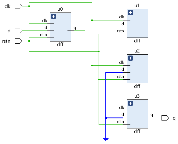
在仿真中,此类未连接的端口将表示为高阻抗 ('hZ),通常在波形中显示为中间垂直对齐的橙色线。
<无脚本>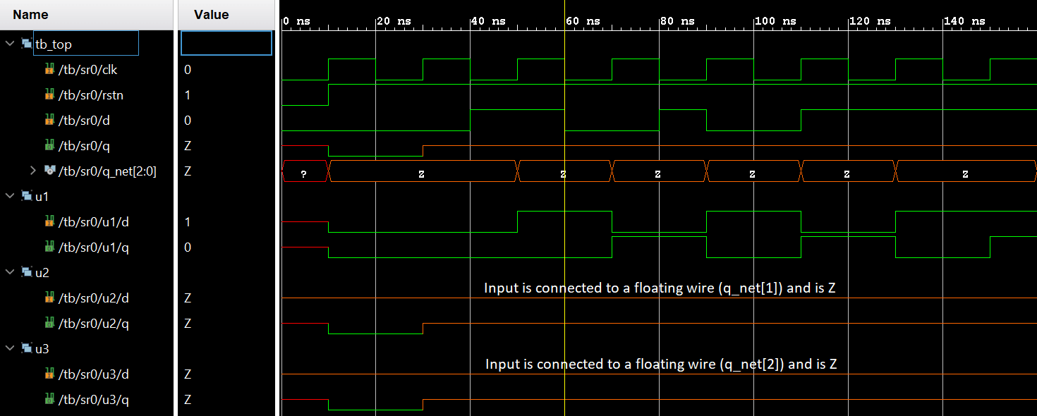
所有端口声明都隐式声明为 wire 因此,在这种情况下,端口方向就足够了。但是 output 需要存储值的端口应该声明为reg 数据类型,可以在像 always 这样的程序块中使用 和 initial 仅限。
input 类型的端口 或 inout 不能声明为 reg 因为它们是不断从外部驱动的,不应该存储值,而是尽快反映外部信号的变化。连接两个具有不同向量大小的端口是完全合法的,但向量大小较小的端口将占优势,而另一个宽度较大的端口的剩余位将被忽略。
	// Case #1 : Inputs are by default implicitly declared as type "wire"
	module des0_1	(input wire clk ...); 		// wire need not be specified here
	module des0_2 	(input clk, ...); 			// By default clk is of type wire

	// Case #2 : Inputs cannot be of type reg
	module des1 (input reg clk, ...); 		// Illegal: inputs cannot be of type reg

	// Case #3: Take two modules here with varying port widths
	module des2 (output [3:0] data, ...);	// A module declaration with 4-bit vector as output
	module des3 (input [7:0] data, ...); 	// A module declaration with 8-bit vector as input

	module top ( ... );
		wire [7:0] net;
		des2  u0 ( .data(net) ... ); 		// Upper 4-bits of net are undriven
		des3  u1 ( .data(net) ... );
	endmodule

	// Case #4 : Outputs cannot be connected to reg in parent module
	module top_0 ( ... );
		reg [3:0] data_reg;

		des2 ( .data(data) ...); 	// Illegal: data output port is connected to a reg type signal "data_reg"
	endmodule
Verilog