

Verilog 赋值语句
wire 类型的信号 或类似的数据类型需要连续分配一个值。例如,考虑用于连接面包板上部件的电线。只要将+5V电池加到导线的一端,连接到导线另一端的组件就会得到所需的电压。

在 Verilog 中,这个概念是由 assign 实现的 任何 wire 的语句 或其他类似的数据类型之类的线可以用一个值连续驱动。该值可以是常数,也可以是由一组信号组成的表达式。
赋值语法
赋值语法以关键字 assign 开头 后跟信号名称,可以是单个信号,也可以是不同信号网络的串联。 驱动力 和延迟 是可选的,主要用于数据流建模,而不是合成到真实硬件中。右侧的表达式或信号被评估并分配给左侧的网络或网络的表达式。
assign <net_expression> = [drive_strength] [delay] <expression of different signals or constant value>
延迟值可用于指定门的延迟,并用于模拟真实硬件中的时序行为,因为该值指示何时应为网络分配评估值。
规则
使用 assign 时需要遵守一些规则 声明:
- LHS 应始终是标量或矢量网络或标量或矢量网络的串联,而不是标量或矢量寄存器。
- RHS 可以包含标量或向量寄存器和函数调用。
- 只要 RHS 上的任何操作数的值发生变化,LHS 就会更新为新值。
assign语句也称为连续赋值,并且始终处于活动状态
示例 #1
在以下示例中,被调用的网络由信号表达式连续驱动。 i1 和 i2 与逻辑与 & 形成表达式。
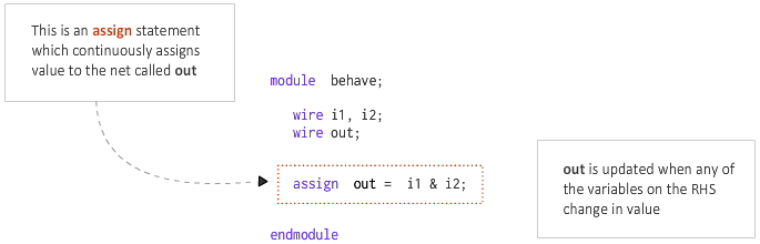
如果将线转换为端口并合成,我们将在合成后得到如下图所示的 RTL 原理图。
<无脚本>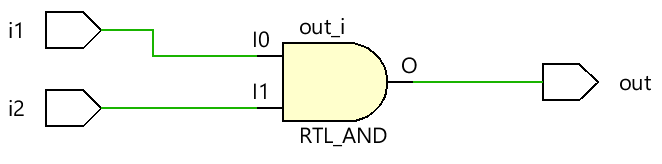
Verilog中可以用连续赋值语句来表示组合门。
示例 #2
下面显示的模块接受两个输入并使用 assign 使用部分选择和多位连接来驱动输出 z 的语句。将每个案例视为模块中的唯一代码,否则很多 assign 同一个信号上的语句肯定会让输出变成X。
module xyz (input [3:0] 	x,		// x is a 4-bit vector net
						input 				y, 		// y is a scalar net (1-bit)
						output [4:0] 	z ); 	// z is a 5-bit vector net

wire [1:0] 	a;
wire 				b;

// Assume one of the following assignments are chosen in real design
// If x='hC and y='h1 let us see the value of z

// Case #1: 4-bits of x and 1 bit of y is concatenated to get a 5-bit net
// and is assigned to the 5-bit nets of z. So value of z='b11001 or z='h19
assign z = {x, y};

// Case #2: 4-bits of x and 1 bit of y is concatenated to get a 5-bit net
// and is assigned to selected 3-bits of net z. Remaining 2 bits of z remains
// undriven and will be high-imp. So value of z='bZ001Z
assign z[3:1] = {x, y};

// Case #3: The same statement is used but now bit4 of z is driven with a constant
// value of 1. Now z = 'b1001Z because only bit0 remains undriven
assign z[3:1] = {x, y};
assign z[4] = 1;

// Case #4: Assume bit3 is driven instead, but now there are two drivers for bit3,
// and both are driving the same value of 0. So there should be no contention and
// value of z = 'bZ001Z
assign z[3:1] = {x, y};
assign z[3] = 0;

// Case #5: Assume bit3 is instead driven with value 1, so now there are two drivers
// with different values, where the first line is driven with the value of X which
// at the time is 0 and the second assignment where it is driven with value 1, so
// now it becomes unknown which will win. So z='bZX01Z
assign z[3:1] = {x, y};
assign z[3] = 1;

// Case #6: Partial selection of operands on RHS is also possible and say only 2-bits
// are chosen from x, then z = 'b00001 because z[4:3] will be driven with 0
assign z = {x[1:0], y};

// Case #7: Say we explicitly assign only 3-bits of z and leave remaining unconnected
// then z = 'bZZ001
assign z[2:0] = {x[1:0], y};

// Case #8: Same variable can be used multiple times as well and z = 'b00111
// 3{y} is the same as {y, y, y}
assign z = {3{y}};

// Case #9: LHS can also be concatenated: a is 2-bit vector and b is scalar
// RHS is evaluated to 11001 and LHS is 3-bit wide so first 3 bits from LSB of RHS
// will be assigned to LHS. So a = 'b00 and b ='b1
assign {a, b} = {x, y};

// Case #10: If we reverse order on LHS keeping RHS same, we get a = 'b01 and b='b0
assign {a, b} = {x, y};

endmodule
分配 reg 变量
驱动或分配reg是违法的 使用 assign 键入变量 陈述。这是因为 reg 变量能够存储数据,不需要连续驱动。 reg 信号只能在像 initial 这样的程序块中驱动 和 always .
隐式连续赋值
当 assign 语句用于为给定的网络分配一些值,它被称为 explicit 任务。 Verilog 还允许在声明网络并调用 implicit 时进行分配 任务。
wire [1:0] a;
assign a = x & y; 			// Explicit assignment

wire [1:0] a = x & y; 	// Implicit assignment
组合逻辑设计
考虑以下由组合门和相应的 Verilog 代码组成的数字电路。
<无脚本>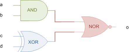
组合逻辑需要连续驱动输入以保持输出,这与触发器等顺序元件不同,触发器的值在时钟边缘被捕获和存储。所以一个 assign 语句非常符合目的,因为只要右侧的任何输入发生变化,输出 o 就会更新。
// This module takes four inputs and performs a boolean
// operation and assigns output to o. The combinational
// logic is realized using assign statement.

module combo (	input 	a, b, c, d,
								output  o);

  assign o = ~((a & b) | c ^ d);

endmodule
硬件示意图
在设计细化和综合之后,我们确实看到了一个组合电路,其行为方式与 assign 建模的方式相同 声明。
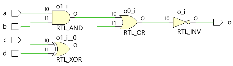
看到只要 RHS 上的组合表达式为真,信号 o 就变为 1。同样,当 RHS 为假时,o 变为 0。输出 o 是从 0ns 到 10ns 的 X,因为输入在同一时间是 X。
<无脚本>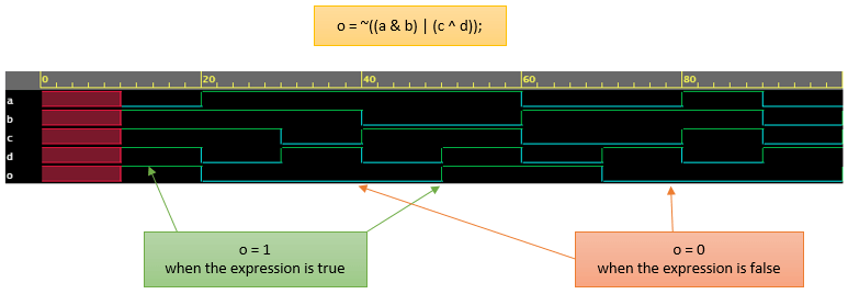
单击此处查看带有模拟示例的幻灯片!
Verilog