

铜 PCB – 如何影响 PCB 板制造
在铜PCB上,PCB可能会出现几种可能的问题,但可以说导致PCB故障的常见原因只有四种:
1.烧毁的组件。
2. 制造不良的组件。
3.环境因素。
4. 年龄。
主要使用铜PCB,因为它解决或减少了这些故障的规律性;对于木质和玻璃 PCB,您必须确保烙铁温度或多或少完美,因为任何更高的温度都可能导致元件烧毁。
铜 PCB 是最容易制造的 PCB 之一,因为所需的材料和组装服务使其易于获得。 WellPCB 可以将 PCB 问题减少到尽可能低,消除诸如烧毁的组件、制造不良的组件和老化等问题。
那么,如何从各个方面保证或使其理想化,让我们看看本指南是否向我们展示了该做什么。
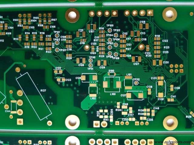
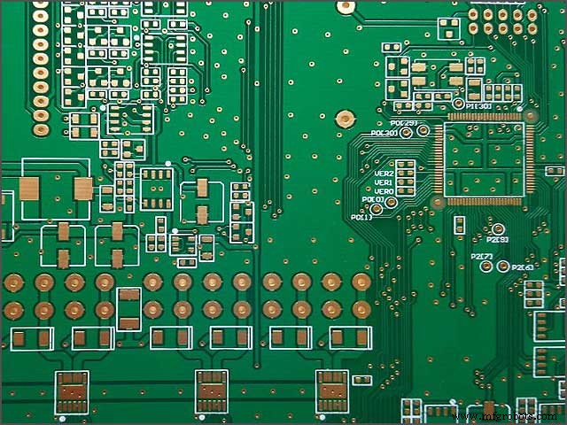
1.铜电路板 —PCB 上的铜
基于其导电性和热阻,铜PCB是其中最常用的。增强材料顶部带有铜结构(覆铜或箔)的 PCB。
或者由于其导电性而将铜作为主要材料。铜PCB因其适应性强而受到工程师的青睐。
人们选择铜 PCB 的原因如下:
1. 提高导热性,从而将热量散布到整个电路板,显着降低烧毁组件的机会
2. 增加导电性
3. 充分利用材料的潜力(您可以使用每个空间,而无需考虑热和电的影响)
4. 再镀一层铜的可能性。
选择铜PCB时不需要太多考虑。只要您对电气工程有深入的了解,您就可以在电视遥控器上使用会说话的泰迪熊玩具中的铜 PCB。
根据 PCB 的类型(单层、双层、多层、刚性、柔性或刚柔性)、厚度和重量变化,有一系列电子产品的标准尺寸。
如前所述,PCB旨在确保电路中有稳定的流动。因此,重量和厚度等因素是重要因素,因为它们从技术上改变了 PCB 的整个处理方式,从焊料类型到烙铁、焊接技术以及您需要的温度。
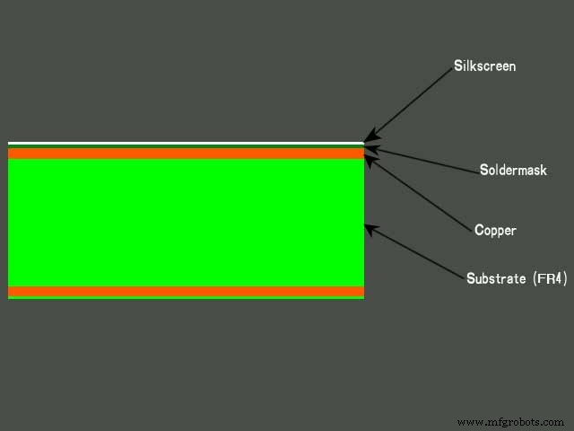
铜PCB的主要成分是:
1.丝印:
这也称为丝网印刷,一种用于在基板上添加墨水(主要是绿色)作为 PCB 上的绘画的印刷技术。
它用于在板上显示字母、数字、符号和图像(电源入口和出口、潜在的微芯片放置、变压器位置、加号和负号-)。通常只使用一种颜色,可见度一般比较低。
2。铜电路板 —阻焊层:
这是 PCB 上的第二层。就是在电路板的铜线上,是聚合物的伪光泽整理层。
它的工作是防止氧化和灰尘或碎屑等环境因素聚集在焊盘之间。阻焊层还有助于防止我们所说的焊桥。当使用烙铁时发生滑动,会发生焊桥,导致两个导体接触。
3.铜:
铜赋予 PCB 卓越的高性能。它为PCB材料提供了表面粗糙度以及铜与介电材料结合时的情况。
两者协同工作为 PCB 提供了出色的性能输出,尤其是在射频和微波频率方面。
铜表示PCB上的信号通路,您看到的电路图案是高精度制作的,只有高质量的铜;与PCB的基板材料结合好就可以生产出来。
铜的热膨胀系数(CTE)约为 17ppm/°C,这是电子设备开始工作时材料所经历的膨胀和收缩量。
4.铜电路板 —基材:
底层中的基板,板基板,通常是介电复合材料,主要由环氧树脂和增强材料(玻璃纤维,有时是织布或非织布,甚至已经使用纸)组成。
对于树脂,已知使用填料状陶瓷。最常见的基材类型是 FR -4(其中 FR 代表阻燃剂);之所以说FR -4 铜是最好的,是因为它具有出色的导电特性,即使在玻璃纤维基材中也能脱颖而出。
FR -4 铜的另一个特点是其高强度、介电性能和表观耐热性。铜与基板的融合对于 PCB 的性能和可靠性至关重要。
2.铜板厚度
如前所述,您需要在使用前始终考虑 PCB 的厚度和重量。
是的,铜 PCB 可以承受更多的热阻和导电性;这并不意味着您在超级计算机上使用用于蜂鸣器的 PCB;这就像试图只用鱼线而不用鱼钩或诱饵来抓鱼;一定的失败。
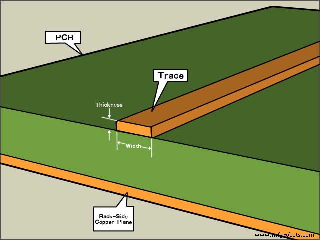
2.1 铜PCB —铜厚单位
其厚度的标准铜测量单位是 Oz。 (盎司)。但是,它可以以英寸为单位。大多数时候,人们不会考虑 PCB 的铜厚度,而是将 1 盎司铜压平并均匀分布在 1 平方英尺区域后整个 PCB 的厚度。
几乎所有印刷 PCB 的铜厚度均为 1 盎司。在 PCB 制造方面,制造商假设为 1 盎司。除非客户提供特定规格,否则他们会引用和构建设计。
一位客户决定设计需要超过 1 盎司的额外电流,可以承载,然后增加铜宽度或您的走线宽度会更好。在某些情况下,成品铜是一盎司。
比外层的起始铜更重要,但对于内层,成品铜相当于起始铜。
通常为 2 盎司。 1 盎司铜的厚度无疑是最熟悉和最标准的铜重量,因为它经常达到既不过分也不过分的程度。铜厚度过大且成本更高,而 0.5 铜可能不够,特别是对于需要承受更高电流的接地层。
因此,1 盎司的铜厚度通常是满足您的设计和财务需求的最合适的选择。
如果您需要更紧密的跟踪和空间,您通常应该这样做;复制需要重铜的层,并确保将铜切成两半。假设您需要 8 mil 线路加上 4 oz 铜,最好的选择是复制该层并使用 2 oz。铜。
用于重 5 盎司的起始铜砝码。或更多,也建议加倍一层而不是更厚的铜。当考虑到较厚铜的加工复杂性时,添加层比使用厚铜便宜。
换句话说,2 层 6 盎司铜板通常比 4 层 3 盎司铜板贵。
2.2 关于铜厚的常见问题
大多数客户提出的第一个问题是基于 PCB 制造商的 BAC-Final-Web-107Minimun 生产线宽度能力。然而,在大多数情况下,铜的重量很少是答案。
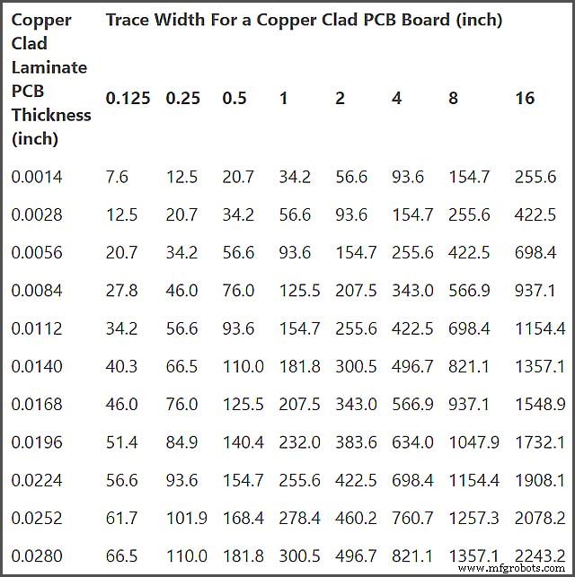
上表显示了铜的厚度关于宽度。
3.铜电路板 —铜 PCB 重量
我们已经讨论过铜 PCB 厚度的重要性;现在,我们将深入了解为什么铜PCB的重量与厚度一样重要。
默认情况下,PCB 的重量始终约为 1.2 盎司。铜,一个0z。镀铜通孔的铜厚和一密耳铜。
| 盎司 | 克 | 微米 |
| 1 | 300 | 35 |
| 2 | 600 | 70 |
| 3 | 900 | 105 |
当然,基础范围为 0.5 盎司。至 3.0 盎司。同时,镀铜的范围为 0.7 盎司。至 2.0 盎司。铜的重量越高,电性能越好,板上的蚀刻工艺也越复杂。
您应该知道重量很重要,它会影响 PCB 的许多方面,例如:
1.可实现的迹线和空间宽度尺寸
2. 建议环形圈的最小宽度
3. 底铜决定线路所需的减量,所以底铜越多,线路减量越多。
在 PCB 设计阶段需要非常注意,这可能会导致 PCB 的成败,尤其是在未说明所需铜的重量时:
1.内层没有功能的焊盘
2. 边缘可以通过公差来避免短路
3.瞄准小孔的负公差
4. 始终考虑铜的厚度。大多数时候,这只是 1 盎司。铜。
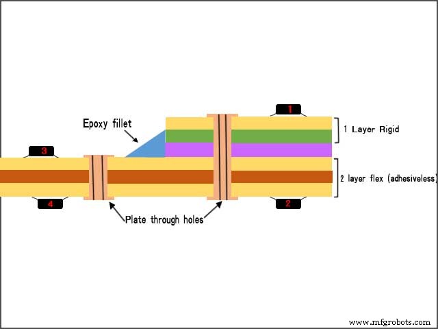
3.1 重铜先进PCB的发展
在用先进的PCB开发重铜时,多层PCB是使用2到5层不同层次的铜层来生产的。哪个是通过使用相似的铜层相互连接的?
额外的铜层增强了电路板的功能,额外的通孔通过保持焊盘良好连接,有助于通过更多电流 PCB。通过将所需的电缆保持在适当的位置,它有助于提高住宅固定螺栓的强度。
还开发了新的低成本制造方法,通过替换伸出表面 20 英里的重铜来为组装提供必要的帮助。
用于重型 PCB 的埋地技术可以在表面上方或板表面下方有任意数量的铜。
3.2 组装大电流 PCB 和厚铜基板
当我们组装更高电流的 PCB 和厚重的铜基电路板时,开发可能具有挑战性,但并非不可能,因为这需要额外的时间和精力。
为了开发这样的板子,工程师需要格外小心地通过观察热传递形式的热传递来设计和开发板子。
需要使用足够高的温度焊接具有重铜的 PCB,并正确焊接以获得更好的效果。强烈建议使用更高温度等级的无铅制造PCB。
会适当地层压它,以帮助保持垫与所有保留的热量相连。
好PCB。我们将为您提供一站式服务和优质产品。您可以将您需要制作的文件发送给我们并立即获得报价!我们还在等什么?我们拥有十年的 PCB 制造经验,已成为中国 PCB 制造初学者或经验丰富的人士最重要的选择。参与这种制造的人可以为他们在国外的客户提供基本功能。
通过选择优惠运输代理的绝佳选择。
好PCB。我们在中国有十年的 PCB 制造经验,由于成本相关问题而获得了发展势头。我们将为您提供一站式服务和优质产品。您可以将您需要制作的文件发送给我们并立即获得报价!我们还在等什么?因为与本地制造商的其他地区相比,在中国制造 PCB 的成本更低。
您可以从 WellPCB 获得服务,因为它们是中国知名的制造商。他们为从小型到大型 WellPCB 的客户提供服务。我们将为您提供一站式服务和优质产品。您可以将您需要制作的文件发送给我们并立即获得报价!我们还在等什么?我们有十年的 PCB 制造经验。
要下订单,建议您浏览他们的网站并通过 Gerber 文件提交所需信息。
建议您指定您在 PCB 制造中需要哪些类型的定制,因为我们有经验为客户提供出色的选择,以额外的价格为您开发定制的 PCB 组件。
该公司拥有经验丰富的资源,可确保您通过我们的投资获得最大的价值。
4.覆铜
关于覆铜 PCB 还没有说什么?您需要询问工程师并看着他继续谈论不可否认但同样重要的优势,以及经济上的便宜;覆铜板是大多数工程师在创建 PCB 时选择的电路板。
覆铜 PCB 使您可以轻松地在电路上焊接组件,因为它是创建的;非常适合设计课程。
与其他电路板相比,覆铜 PCB 材料的竞争性使其易于定制电路板的尺寸和形状。由于它们可用的材料,与其他 PCB 的成本相比,它会导致电子设备的成本下降。
在覆铜PCB的众多应用中,其中一些已经被提及。覆铜PCB通常用于武器控制系统、雷达系统的电源、大功率平面变压器的初级和次级绕组、配电板以及电池充电器和监控系统。
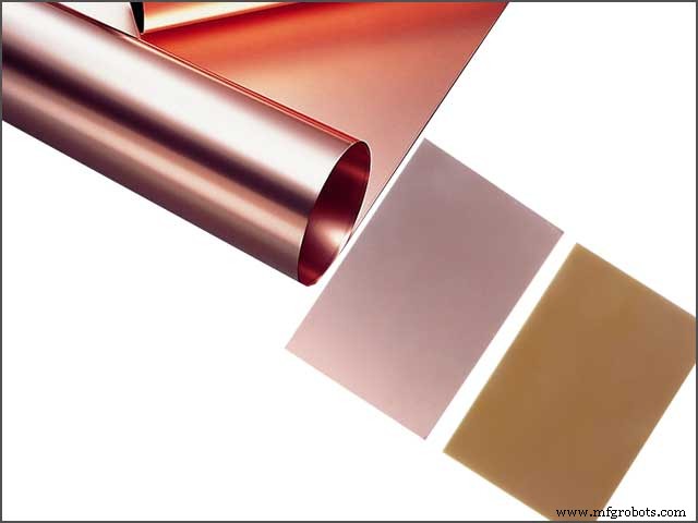
4.1 铜PCB —覆铜板:
简称CCL(Copper Clad Laminate),是指以木浆纸或玻璃纤维浸泡树脂和增强材料制成的基材。
覆铜板可分为:
- 1.CCL基于机械刚性——这种CCL是刚性的
- 2.基于有机树脂绝缘的覆铜板。
- 3.覆铜板根据厚度一般为0.55毫米左右
- 4.绝缘树脂覆铜板。
CCL有不同的类型
它们根据机械刚性、绝缘材料、厚度和增强材料类型等不同的分类标准进行分类。
- 1.按机械刚性: 您有刚性 CCL(G10、FR-4、CEM -1)和柔性 CCL,刚性 PCB 取决于刚性 CCL,而柔性 PCB 取决于柔性 CCL。
- 2.按绝缘材料: 您有有机树脂覆铜板、金属基覆铜板、陶瓷基覆铜板等等
- 3.按厚度: 您有标准厚 CCL 和薄 CCL,厚 CCL 我们要求> 0.5mm 厚度,对于薄 CCL,我们要求 <0.5mm 厚度
- 4.按增强材料: 我们有玻璃纤维基材(FR -4)、纸基材(XPC)、复合覆铜板(CEM -1、CEM -3)。
- 5.应用绝缘树脂: 我们有环氧树脂覆铜板(FR -4,CEM -3)和酚醛覆铜板(FR -1,XPC)。
4.2 铜PCB —快速提问:什么是优秀的 CCL?
很简单,优秀的 CCL 需要满足特定要求才能称为 EXCELLENT,其中包括
♦ 外观:
do you like dents and scratches in your car? Guessing no, well same for CCL; a cut, gash, wrinkle, or pinholes can lead to low performance in the CCL and turn the PCB. So the smoother and cleaner the job, the better the performance.
♦ Size:
Your CCL is a base material for the PCB; it needs to conform to the size requirement of the PCB.
♦ Electrical Performance:
this is the primary mission of the CCL which means it’s the primary mission of the PCB; specific details have to be paid to the Volume Resistance, Insulation Resistance, Dielectric constant, Arc resistance, and so on.
♦ Physical Performance:
In physical performance, it’s always noteworthy to consider the bending strength, thermal stress, heat resistance, and punching quality.
♦ Chemical Performance:
The requirements needed to be met by the CCL are flammability, dimension stability.
♦ Environment Performance:
The CCL should meet water absorption standards.
Within the CCL is what we call a prepreg, which is reinforced material; it is the reinforcement material used in a CCL. It is made of fiber and is referred to as the bonding sheet. It is mainly made of fiber cloth, epoxy resin, acetone, and many others.
Using quality prepreg results in high-quality CCLs, which enhances the quality of PCB. The quality of the prepreg material used depends on the resin content, resin fluidity, and dicyandiamide crystallization. Consequently, you should select resin based on the quality and the cost.
The cost should be related to the thickness of the fiber cloth. Thinner prepreg is recommended even though it might be a little bit costly.
To meet Restriction of Hazardous Substances Regulations, it is recommended that you look at the reliability and heat resistance of the CCls. The latest CCL has been enhanced by modifying them so that they:
Include Halogen-free CCL – refers to CCL with the content of bromine and chlorine controlled within 900ppm. Care should be taken so that the content does not exceed 1500ppm.
Lead-free CCL – refers to Copper laminate with surface mounting that has been carried out without applying lead-free solder. The epoxy resin may be used, but the RoHS regulations must be adhered to. Note that RoHS prohibits the use of substances such as PBDE and PBBD substances.
4.3 Classification Of Resin
Resins used in CCls could be classified as:
- Epoxy resin
- Phenolic resin
- Polyamide resin
- Bismaleimide triazine
- Phenolic resin
If you are using fiber, the following quality aspects should be considered:
- Humidity resistance
- Intensity
- Insulation capability
- Heat and fire resistance
4.4 Copper PCB —Copper Laminates
This is the used clad that is over the dielectric layer and substrate (resin composite material).
The copper acts as a composite insulator material while being a good conductor, also remember. You can have rigid or flexible base material. Still, the primary purpose of the copper laminate is to act as mechanical support for the pin, i.e., the firm base that holds the electronic component and joins them at the same time.
The most popular types of copper laminates used for PCB are:
♦Polyimide:
This is a base material used for high-temperature PCB applications; it has an excellent glass transition (Tg =220 °C) that gives it an outstanding performance over high temperatures. It allows for soldering and desoldering of components, giving you more legroom for mistakes.
♦Phenolic:
This base material is used in low-cost applications with the FR-2, CEM-1, or CEM-3 brand names. It is most widely used in single-layer PCB of small household gadgets and appliances. It is slightly brittle but hard to bend.
♦Arlon:
So far, it’s one of the most devise base materials with different applications just behind the FR -4; it is the preferred base material for multilayer PCBs; you find them in military, wireless, and communication systems.
♦FR-4:
This is a glass fiber base material that is durable, hard to bend, and cut with fire retardant qualities; it’s Tg =160°C. Because of all these qualities, various applications within single, double, and multilayer PCBs are used for power supply, mixed-signal and digital applications.
Other Copper Laminates used are Tetrafunctional epoxy, Thermount, and cyanate ester.
For electrically interconnecting the components, the laminates can be nickel, stainless steel, aluminum, and copper. However, the most widely used material for lamination purposes is copper. The aluminum found commercial applications recently and is appreciated in low-cost home appliances.
The conductive cladding layer is skinny and is over one or both sides of the resin composite material. The thickness of the cladding material is determined by how much material is deposited regarding weight.
It is a simple process but requires that you take some precautions. First, you need to turn the laminator on before feeding the board and the film in the machine. The side with the excess border should be provided into the laminator.
In most cases, you are required to put the board into the machine for the second time if you want to improve the quality of your clad board. It means that the board should be put back into the laminator immediately after it finishes the first run.
The same procedure should be used if you are working on a double-sided board.
5. Copper PCB —Copper Layer Design
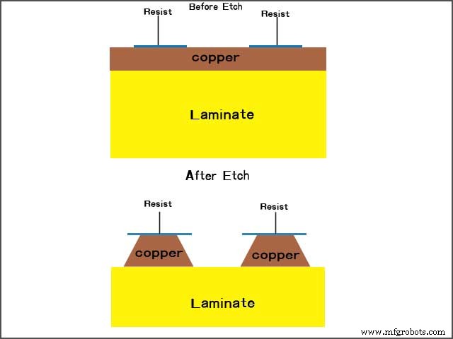
A keen eye is kept by designers when designing copper PCB; a designer must think in reverse. A board starts as solid copper; then, you remove the bits you don’t want.
It is faster to build, less expensive, and consuming when the copper is the same size as the board. Some techniques can make much difference from a frustrating experience to a smooth experience.
Maximizing copper is most common in two ways:
• Manually:
By specifying the specs of your PCBs (shape and size), this method is faster but sloppy as copper can be placed as an object, and these objects are checked for minor errors when assigned to a net. This method is mainly used for quick turns or prototype builds.
• Automatically:
However, this method is more time-consuming than the manual process, but the pour method helps to maximize copper. Copper will be left behind by drawing a border around the board area and pouring the copper in, laying out the board, and going back and placing copper shapes to fill it.
What you need to know is that when the copper pour is used, you define your boundary and everything inside when the pour operation is performed while connected automatically.
This method usually favors a large area, several irregularly shaped objects, or unusual shapes. The pour operation automatically fills the unique body while additionally isolating other traces in the area.
Objects that the copper pour can automatically handle are Traces, nets, decals, and pads. When used right, you don’t need much; the copper pouring will make the right moves and connections; you can double-check using the continuity check tool.
Now we have talked about both the manual and automatic methods, and you probably think the manual process is the best, especially for the short time sprint. Still, in the long run, the intuitive approach can be better even though it is works upfront.
There are three situations when using a copper pour might be the better option for your design.
1. Polygon Management
Manual – when you’re dealing with regular polygons, this method could be time-consuming and messy. A quick fix would be to drop overlapping shapes on top of each other to build your required profile.
It is quick, but it’s a short-term solution as eventually, you will need to do vertex editing to clean the design.
Automatic – The copper pouring method here is a “no-brainer” because we deal with complex shapes; this process is automatic. By defining the border and running copper, you eliminate the tedious job of re-editing later.
2. Plane Management
Manual – A plane is a large area of copper where all connections are one net. If you intend to build a board with separate planes while changing parts often, you often recommend route traces point to point.
Automatic – An excellent way to avoid several traces that all go to the same point is to use a copper pour method design on a plane for the ground. This will automatically connect all the connections on one network.
3. Thermal Management
Manual – if you have a Hot board with much space, the best way to cool it down is to add a copper square to help conduct the heat away. Which may not always be the case?
Automatic – when you define the area around the critical parts of the board, prioritizing them, you can minimize the thermal stress. This method is used when importance is placed on maximizing the copper surface area.
6. PCB Copper Plating And Cleaning
6.1 Copper PCB —Plating
Plating is very important to a PCB board. If all the traces on the external layers are not protected, the copper PCB will oxidize and deteriorate, making the board unstable. How do you know your copper has corroded? It will turn green. The two main reasons for plating are also called copper coating and surface finish:
1. To protect exposed copper circuitry
2. To provide a surface good enough for soldering when assembling components to the PCB.
You have various PCB copper plating options to choose from, and each carries its advantages and disadvantages. You can find them here.
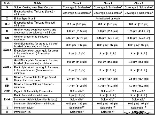
There are IPC standards for surface plating which is shown below:
6.2 Copper PCB —Clad Board Cleaning
Getting the best results is essential for you to clean your board using fine wool. You may also choose to use an abrasive pad before rinsing it with water. It helps to remove the dirt and any other contamination.
Alternatively, you may start by cleaning the dry board by exposing it to heat for about 5 minutes. This way, it ensures that the board is clean and ready for the film.
Conclusion
But I can answer you with one sentence “Copper PCB is the most reliable, effective PCB used across the most electronic device,” you don’t need to take my word for it. Just take a look at your phones.
And we at WellPCB are here to meet your needs at any time.
工业技术