

研究单个 Si 纳米线的尺寸相关导电特性
摘要
通过纳米球光刻结合金属辅助化学蚀刻成功地制造了周期性排列的垂直排列的硅纳米线 (Si NWs) 阵列。通过调整蚀刻时间,可以很好地控制纳米线的直径和长度。通过对单个纳米线的导电原子力显微镜 (CAFM) 研究此类 Si NW 的导电性能,特别是它们的尺寸依赖性。结果表明,Si NW 的电导与其直径和长度密切相关。具有更小直径和更短长度的 Si NW 表现出更好的导电性能。连同 I-V 曲线表征,从与尺寸相关的肖特基势垒高度的角度来看,假设了一种可能的机制,静电力显微镜 (EFM) 测量进一步验证了这一点。该研究还表明,CAFM 可以作为探索导电性能对单个纳米结构的尺寸(或其他参数)依赖性的有效手段,这对于纳米结构的制备优化和潜在应用都是必不可少的。
介绍
硅纳米线(Si NWs)由于其高纵横比和独特的电、热电和光电特性,以及与传统硅技术的兼容性,在电子、光子、光电等许多领域获得了广阔的应用[1,2,3] ,4,5]。在过去的几十年中,Si NWs 的研究主要集中在生长改进和性能测量上。已经开发了许多制备 Si NW 的方法,包括自下而上的方法,如汽-液-固法、化学气相沉积和分子束外延 [6,7,8,9,10] 和使用电子的自顶向下方法。 -光束光刻、反应离子蚀刻或金属辅助化学蚀刻 [11,12,13,14,15,16]。在这些方法中,纳米球光刻 (NSL) 与金属辅助化学蚀刻 (MACE) 相结合,因其简单、低成本和多功能性而被广泛用于制造大面积垂直排列的硅纳米线有序阵列 [15,16,17] ,18,19,20,21,22,23]。 MACE获得的Si NWs通常具有非常粗糙甚至多孔的表面[18,19,20,21],这使得它们具有较大的比表面积和优异的性能,在生物传感器、热电器件、锂-离子电池、太阳能电池等 [22,23,24]。要实现这些应用,必须充分了解它们的电气特性。目前,有两种方法常被用于研究纳米线的电学特性。一种是通过普通的宏观方法进行的,这种方法相对容易,但只能提供大量纳米线的平均结果 [24, 25]。另一种是使用特殊制造的单纳米线器件对单个纳米线进行 [21, 26,27,28],这可以排除尺寸不均匀性的影响,但不容易实现,尤其是在测量属性依赖性时。因此,迫切需要更方便的方法来研究单个纳米线的电学特性,而无需复杂的纳米加工。
近几十年来,基于扫描探针显微镜 (SPM) 的电学测量表明它们是用于纳米级电学表征的强大技术 [29, 30]。在这些 SPM 技术中,导电原子力显微镜 (CAFM) 已成功应用于研究单个或单个纳米结构的导电性能 [30,31,32]。已经报道了对各种纳米线的 CAFM 研究,例如 ZnO、InAs、CdS、CdSe、GaAs、InAsSb 和 Si NWs [33,34,35,36,37,38]。虽然大多数研究都集中在具有固定参数的纳米线的导电性能上,但也进行了一些研究来探索导电性能的掺杂依赖性 [37,38,39]。纳米线的导电性能的尺寸相关性的研究还少得多。只有少数关于纳米线直径相关导电特性的研究报道,甚至不限于 CAFM,其中相当一部分涉及纳米线电阻率的直径相关性 [25, 40,41,42]。例如,一些关于 GaN 纳米线的研究发现,在临界直径(20 ~ 80 nm,取决于制造方法)处电阻率很高,并且在此之后保持不变 [41, 43],而其他关于 Si 纳米线的研究报告说纳米线的电阻率随着直径在几十到几百纳米范围内的增加而降低 [40, 44]。对于具有金属触点的半导体纳米线,肖特基势垒可能对其导电性能起重要作用。因此,除电阻率外,在半导体纳米线存在的情况下,肖特基势垒也应考虑在内。有几篇论文关注肖特基势垒高度 (SBH) 的直径依赖性,但结果并不一致。例如,Calahorra 等人。通过求解纳米线中的泊松方程计算 SBH,发现势垒高度随着尺寸减小而增加的明显趋势 [45]。 Soudi 等人通过实验报告了类似的直径依赖性。在研究 ZnO 单纳米线器件上与直径相关的表面光电压和表面态密度时。他们发现表面势垒高度随着直径的减小(20-60 nm)而增加,这可以通过使用泊松方程 [46] 模拟的表面态密度来解释。相比之下,Yoon 等人对单个 Si 纳米线场效应晶体管的扫描光电流显微镜测量。揭示了相反的依赖性,即由于界面态的贡献,势垒高度随着直径的减小而减小[47]。毛等人的另一项实验工作。在单个 Pt/ZnO 纳米针肖特基二极管上也报告了势垒高度随着直径的减小而减小,这可以通过焦耳热效应和/或界面的电子不均匀性来解释 [48]。因此,迄今为止,纳米线导电性能的直径依赖性尚未达成共识,也远未得到彻底了解。特别是,通过MACE方法制备的单个Si NWs具有与尺寸相关的导电性能以及与尺寸相关的SBH研究尚未报道,其表面相当粗糙,具有广阔的应用前景。
在本文中,通过NSL结合MACE的方法制备了具有不同直径和长度的垂直排列的Si NW的周期性阵列。通过调整蚀刻时间,可以很好地控制 SiNW 的直径和长度。 CAFM 无需任何进一步的纳米加工即可研究阵列内单个 Si NW 的导电性能,只需更换样品即可方便地研究单个 Si NW 的尺寸依赖性导电性能。结果表明,在单个 Si NW 上测量的电流强烈依赖于 NW 的直径和长度。具有更小直径和更短长度的 Si NW 表现出更好的导电性能。通过 I-V 曲线拟合,可以获得与尺寸相关的肖特基势垒高度,这是确定纳米线与尺寸相关的导电性能的关键因素。此外,通过静电力显微镜 (EFM) 测量获得了类似的尺寸依赖性 SBH。因此,我们的研究不仅揭示了Si NWs的尺寸依赖性,而且表明CAFM可以作为探索导电性能对单个纳米结构的尺寸(或其他参数)依赖性的有效手段。
材料和方法
材料
Si 晶圆购自 MTI(中国)。聚苯乙烯球体(PS,直径 490 nm)的悬浮液(2.5 wt% 在水中)购自杜克科学公司(美国)。用于制备硅纳米线的丙酮、甲醇、硫酸、过氧化氢和氢氟酸购自国药集团化学试剂(中国)。去离子水(DI,18.2 MΩ·cm)来自超滤系统(Milli-Q,Millipore,Marlborough,MA)。
Si NW 的制造
垂直有序的硅纳米线阵列是由 NSL 结合 MACE 制造的,这在以前的文献 [49, 50] 中有详细描述。主要制造过程安排在图 1a 中。首先,将直径为 490 nm 的单层聚苯乙烯球 (PS) 自组装到化学清洁的平面 Si 晶片(n 型,0.01 Ω cm)上,形成六边形密堆积单层。随后,用O2气体(20 sccm)通过反应离子蚀刻(RIE,Trion Technology)(50 W,70 mTorr)蚀刻PS覆盖的样品以减小PS的直径,PS在以下步骤中充当掩模层。然后,通过离子溅射将 20 nm 的 Au 膜沉积到由 PS 层掩蔽的样品上,作为后续 MACE 处理的催化剂。样品在室温下在HF(40%)和H2O2(30%)混合溶液(体积比4:1)中通过MACE处理。在MACE工艺中,被Au覆盖的Si表面被有效蚀刻,而被PS(无Au)覆盖的Si表面受到保护,从而形成Si NW。最后,将样品分别浸泡在 KI/I2 和四氢呋喃溶液中,去除残留的 Au 层和 PS 球。采用这种制备方法,可以获得大面积周期性排列的垂直排列的Si NW阵列。
<图片>
一 制造垂直排列的硅纳米线阵列的程序示意图。 b 单根Si纳米线CAFM和EFM测量实验装置示意图
Si NW 的表征
通过扫描电子显微镜(SEM,SIGMA300)检查制造的 Si NW 的形态,同时通过拉曼光谱(Jobin Yvon HR-Evolution 2 系统)研究其结构特性,激发波长为 532 nm,低功率约为 1 mW .
如图 1b 所示,使用商业 SPM 设备(Multimode V,Bruker Nano Surfaces)通过 CAFM 和 EFM 研究了 Si NW 的电性能。 Cr/Pt 涂层尖端(Multi75E-G,Budget Sensors,半径约 25 nm)用于 CAFM 和 EFM 测量。在 CAFM 中,导电尖端以接触模式在样品表面上扫描,当尖端接地时,将直流偏置电压施加到基板上,并测量尖端和样品之间的电流。由于在正样品偏置下表面阳极氧化严重,因此所有电流图像都是在负样品偏置下测量的。在 CAFM 实验中测试了范围从 - 0.5 到 - 3.0 V 的各种负电压。发现当偏置电压设置在- 1.5 V以下时,电流太小而无法检测到电导差的样品。虽然偏置电压设置为 - 2.0 V 或更大,但测量结果不稳定,可能是由于在大静电场下尖端和/或样品损坏。因此,电流图像测量选择了 - 1.5 V 的偏置电压。 EFM 测量是在双通道模式下对 Si NW 进行的。在第一次通过时,它在敲击模式下工作以获得地形图像,而在第二次通过时,尖端被抬高到足以忽略范德瓦尔斯力。在提升通道中,在样品和接地尖端之间添加直流电压,并检测静电力引起的相移信号。所有实验均在流动的 N2 环境中进行,以进行稳定的电学测量,并将样品预浸在 HF 溶液(5%)中 30 s,以有效降低氧化层对导电特性的影响。由于测量是在 HF 浸渍后立即进行的,因此重整的氧层应该足够薄以被导电尖端穿透,并且其对电导的影响最小。
结果和讨论
Si NW 的制造
大面积垂直排列的有序硅纳米线阵列的制造如图 1a 所示。通过改变 RIE 时间,PS 球的直径可以减小到所需的值,因此可以实现直径可控的 Si NW。在 90、120 和 150 秒 RIE 蚀刻后获得的 Si NW 的 SEM 图像分别显示在图 2a、b 和 c 中。可以观察到,Si NWs 以大面积的周期性六边形排列垂直排列。这些垂直排列的 Si NW 具有相同的周期 490 nm 和相同的长度约 350 nm(相同的 MACE 时间为 40 s)。 (a)、(b) 和 (c) 中 Si NW 的直径分别约为 350、260 和 190 nm。 NW 直径对 RIE 蚀刻时间的依赖性绘制在图 2d 中,显示出良好的线性相关性。另一方面,可以通过改变 HF 和 H2O2 混合溶液中 MACE 的时间来调整纳米线的长度。图 2e 显示了 40、60、80 和 100 s MACE 后 Si NW 的横截面 SEM 图像。可以看出,随着 MACE 时间的增加,NW 的长度从 350 增加到 960 nm。类似地,Si NW 的长度对 MACE 时间表现出良好的线性依赖性,如图 2f 所示。这些结果表明,采用NSL结合MACE的方法成功制备了直径和长度可控的有序Si纳米线。
<图片>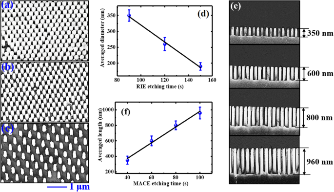
相同长度为 350 nm 但a 直径不同的 Si NW 的俯视 SEM 图像 350 nm; b 260 nm;和 c 190 nm。 NWs 直径对 RIE 蚀刻时间的依赖性绘制在 d 中 . e 相同直径为 260 nm,但不同长度为 350、600、800 和 960 nm 的 Si NW 的横截面 SEM 图像。 f 呈现 NW 长度对 MACE 时间的依赖性
从SEM图像还可以发现,化学蚀刻后的Si NWs表面非常粗糙,其侧壁表面特别粗糙。为了检查作为直径和长度函数的表面层的微观结构,在具有不同直径和不同长度的块状 Si 和 Si NW 上测量了拉曼光谱。使用520 cm − 1 处的最大峰强度对每个光谱进行归一化 ,不同直径和不同长度的结果分别如图 3a 和 b 所示。体硅的光谱显示出一个尖峰位于~ 520.1 cm − 1 .峰位置的红移和峰宽的加宽(称为半峰全宽,FWHM)都可以在 Si NW 上观察到,如图 3c 和 d 所示。对于 350 和 600 nm 较短长度的纳米线,峰值红移和展宽相当小,并且随着纳米线长度增加到 800 nm 及以上而变得相对明显。这种拉曼峰红移和加宽有时归因于掺杂剂水平或晶体含量的变化。根据之前的文献 [5, 51],对于通过相同 MACE 方法制造的 Si NW,掺杂浓度可以具有与起始晶片相同的掺杂水平。由于设备限制,我们无法确认这一结果。另一方面,虽然这些 Si NWs 具有粗糙的表面,但先前的文献发现通过 MACE 方法制造的 Si NWs 可以主要保持其晶体结构,用于 n 和 p 掺杂以及轻掺杂和重掺杂 [5, 51 , 52]。在 NW 的壁表面上仅观察到薄的非晶层。不同组别在不同直径和长度的 Si NW 上获得了类似的结果。因此,可以假设通过 MACE 方法制备的 Si NWs 可以保持其掺杂水平和晶体含量与它们的体对应物几乎相同,除了薄的表面层。
<图片>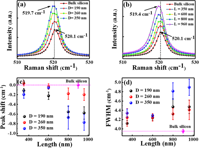
具有a的体硅和硅纳米线的典型拉曼光谱 相同的长度 350 nm 但不同的直径和 b 相同的直径为 190 nm,但长度不同。 c 和 d 表示峰值位置的红移和作为纳米线长度函数的 FWHM 加宽
因此,拉曼峰位移和展宽很可能是由纳米线损坏的粗糙表面引起的 [53]。有几篇论文报道了通过相同的 MACE 方法制造的 Si NW 的拉曼结果。例如,Feser 等人。发现在 520 cm − 1 处显着的峰展宽 随 MACE 时间而增加,并将这种峰展宽归因于蚀刻过程引起的晶体无序(例如,点缺陷簇)[23]。拉瓦迪等人。发现拉曼红移随着 MACE 时间增加,即。 e. TO拉曼峰位于521.1 cm − 1 对于块状硅并移至 518.7 cm − 1 分别用于 80 分钟蚀刻样品 [54]。他们指出,拉曼位移的起源可能是由于在纳米线壁上形成了硅纳米晶体。林等人。观察到TO拉曼峰从520移到516 cm − 1 当 NWs 的长度从 0(块状 Si)增加到 2.73 μm,而峰宽从 3 扩大到 9 cm − 1 随着 NW 的长度从 0.19 增加到 2.73 μm [55]。他们认为拉曼峰展宽主要由声子-应变相互作用决定,拉曼峰位移被证明与应变引起的表面晶格畸变成正比。由于 HF 蚀刻引起的应变随着 NW 的长度(更多蚀刻时间)而增加,拉曼峰红移和加宽都随着 NW 长度的增加而增加。在我们的例子中,从图 3a 和 b 所示的拉曼光谱中,我们可以发现 TO 拉曼峰从 520 到 519.4 cm − 1 当 NW 的长度从 0(块状 Si)增加到 960 nm,而 FWHM 从 4.41 加宽到 4.47 cm − 1 随着 NW 的长度从 350 增加到 960 nm。我们更喜欢这种依赖于长度的拉曼峰位移和加宽源自受损表面(应变或无序)。然而,由于具有不同直径和不同长度的纳米线(<1.0 cm − 1 ),应变/紊乱随尺寸的变化可以认为是最小的。因此,应变/紊乱可能会改变纳米线的电导,但其对电导大小依赖性的影响在下一节中不涉及。
单硅纳米线的导电性能测量
Si NWs 的导电性能是通过 CAFM 在具有不同直径和长度的单个 NWs 上测量的。图 4a、b 和 c 分别显示了长度相同 350 nm 但直径不同 350、260 和 190 nm 的垂直排列的 Si NW 的典型形貌图像,而它们对应的当前图像则是在样品处获得的- 1.5 V 的偏置在 (d)、(e) 和 (f) 中呈现。应该注意的是,由于 Cr/Pt 涂层的 AFM 尖端是一个大角度的楔子,Si NW 的直径比它们的实际直径更大。此外,由于尖端可能无法与基板接触,因此无法很好地检测出纳米线的电流,因此仅考虑在纳米线上测量的电流。从当前图像可以看出,Si纳米线的大部分边缘表现出比中心更好的电导率。这可能是由于 AFM 尖端和 Si NW 之间具有较大接触面积的侧面接触造成的。另外,由于顶面明显的粗糙,中心区域的一些区域也可能出现类似于边缘的大电流,导致没有明显的环状电流分布。另一方面,Si NWs 的电导显然与纳米线的直径有关。可以看出,纳米线的导电面积比和绝对电流值都随着直径从 350 减小到 190 nm 而显着增加。结果表明,具有较小直径的 Si NW 比具有较大直径的 Si NW 更具导电性。为了更直观地获得直径依赖性,图 4g 中显示了沿图 4d 到 f 中标记线的电流剖面。它清楚地表明,直径为 190 nm 的 Si NWs 比直径为 260 nm 和 350 nm 的 Si NW 导电得多。这种直径依赖性也可以从具有不同直径的 Si NW 上的电流分布的统计直方图获得,如附加文件 1:图 S1(a) 所示,当直径减小时,电流分布会转移到高值。平均电流 (I av) 的 Si NWs 是通过对电流图像中所有纳米线的电流进行平均来计算的,这在图 4h 中绘制为 NWs 直径的函数。当 NWs 的直径从 350 减小到 190 nm 时,Si NWs 的平均电流表现出惊人的 9 倍增加。在单条 InAs 纳米线和单条 Si 纳米线器件上已经实现了类似的电流对直径的依赖性 [35, 47]。
<图片>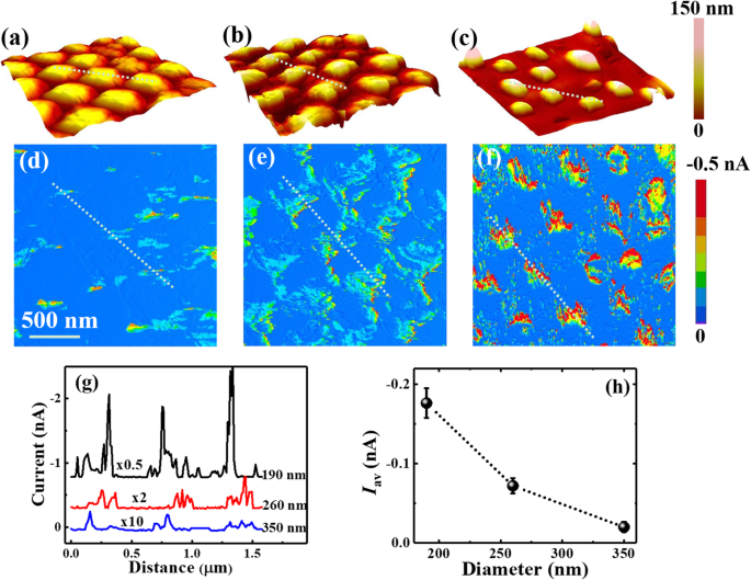
相同长度350 nm但不同a直径的Si NW的形貌图像 350 nm,b 260 nm,c 190 nm。在- 1.5 V的样本偏置下获得的相应电流图像在d中给出 , e 和 f , 分别。 d 中沿标记线的当前配置文件 –f 在 g 中绘制 , 和 h 表示平均电流 (I av) 在纳米线上作为 NW 直径的函数。在a的地形图中添加了相应的线条 –c 和 g 中的剖面曲线 为引导而垂直移动
在- 1.5 V的样品偏压下测量的不同长度和相同直径190 nm的Si NW的典型电流图像如图5所示。图5a至d显示了长度为350的Si NW的电流图像,分别为 600、800 和 960 nm。可以看出,在这些电流图像中,导电面积随着长度的增加而明显减小,而绝对电流的减小并不那么明显,特别是对于长度为350 nm和600 nm的NW。可能由于局部不规则表面粗糙度的存在,在图5b中的某些点观察到更大的电流。然而,图 5b 的平均电流远小于图 5a。使用与上述相同的分析,沿标记线的电流分布如图 5e 所示,统计直方图显示在附加文件 1:图 S1(b) 中。随着 NW 长度的增加,它们都清楚地表现出显着的电流下降。纳米线的平均电流作为 NW 长度的函数绘制在图 5f 中,它们在数十到数百 pA 的数量级上,这远小于图 5a 至 e 中所示的 nA 数量级.这是因为当大多数区域不导电时,纳米线仅在少数导电点处表现出较大的电流。从图 5f,当长度从 300 增加到 960 nm 时,平均电流表现出三倍以上的下降,表明纳米线的电导随着长度的增加而下降。纳米线电阻对长度的依赖性先前已经通过对半导体纳米线的四点电阻测量进行了研究,这表明在欧姆接触下,纳米线的电阻随着电阻率的斜率线性增加而增加 [56, 57]。在我们的例子中,从附加文件 1:图 S2 中给出的 I ~ 1/L 图中,依赖性是显着的非线性;因此,不能从曲线斜率正确地获得电阻率。在 CAFM 测量中值得注意的是,总测量电阻包括 Cr/Pt 涂层尖端和 Si NW (R tip/NW),Si NW (R NW) 和 Si 晶片的电阻 (R 大部分)。由于CAFM测得的电阻主要来自尖端下方的局部表面积,并且随着电流路径上面积的增加而迅速减小,R 与 R 相比,bulk 小得多 西北和 R 小费/西北。另一方面,由于尖端和纳米线之间的金属-半导体接触面积非常小,接触电阻 R tip/NW 远大于纳米线电阻 R 西北。电流依赖于 1/L 的非线性仅表明存在大的接触电阻。因此,在CAFM进行的测量中,应着重考虑金属-半导体接触电阻,其中肖特基势垒起着重要作用。
<图片>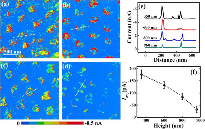
Si NWs在- 1.5 V的样品偏压下的当前图像,具有相同的直径190 nm但a的不同长度 350 nm,b 600 nm,c 800 nm 和 d 分别为 960 nm。沿着 a 中标记线的当前配置文件 –d 在 e 中绘制 , 和 f 呈现纳米线的平均电流 (I av) 作为 NW 长度的函数。 e 中的剖面曲线 为引导而垂直移动
为了验证上述推论,在单个 Si NW 上记录了电流 - 电压 (I-V) 曲线,以研究金属尖端/Si 纳米线接触处的肖特基势垒。具有相同长度 350 nm 但不同直径的 Si NW 上的典型 I-V 曲线如图 6a 所示,而具有相同直径 190 nm 但不同长度的 Si NW 上的典型 I-V 曲线分别显示在图 6b 中。所有 I-V 曲线在负采样电压区域都表现出更大的电流,这与金属尖端和 n 型半导体之间的肖特基接触的典型 I-V 曲线一致。由于 I-V 曲线表现出良好的金属-半导体特性,这表明氧层对电导的影响并不严重,因此在以下讨论中假设为最小。同时,结果表明更小和更短的纳米线比更大和更长的纳米线表现出更大的电导,这与从当前图像获得的结果非常一致。对于定量分析,采用了众所周知的金属-半导体接触热离子发射模型 [58, 59]。在该模型中,在存在串联电阻的情况下,肖特基接触到 n 型半导体的 I-V 特性可以近似为 [59]:
<图片>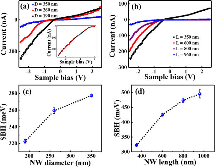
具有相同长度 350 nm 但不同直径的 Si NW 上的典型 I-V 曲线 (a ) 和相同的直径 190 nm 但不同的长度 (b )。 a 中的插图 显示了直径为 190 nm 和长度为 350 nm 的 Si NW 的典型拟合结果。 c 和 d 分别表示拟合结果得到的肖特基势垒高度与 NW 直径和长度的函数关系
$$ I={I}_S\left[\exp \left(\frac{q\left(VI{R}_S\right)}{\mathrm{n} kT}\right)-1\right], $ $ (1)其中 n 是理想因子,R S 是串联电阻。 我 S为饱和电流,可表示为:
$$ {I}_S=\mathrm{AA}\ast {T}^2\exp \left(-\frac{\varphi_B}{kT}\right), $$ (2)其中 A 是接触面积,A* 是理查森常数,φ B 是金属尖端和 Si 纳米线之间的肖特基势垒高度 (SBH)。因此,SBH 可以通过以下公式获得:
$$ {\varphi}_B=kT\ln \left(\frac{\mathrm{AA}\ast {T}^2}{I_{\mathrm{S}}}\right), $$ (3)图 6a 和 b 中的 I-V 曲线可以通过等式很好地拟合。 (1),前部区域的典型拟合线如图 6a 的插图所示。为了从饱和电流获得 SBH 值,假设有效理查森常数 A* 近似等于体硅的常数,即 112 A cm − 2 K − 2 对于 n 型硅 [59]。假设接触面积为 2 × 10 − 11 厘米 2 通过将 Cr/Pt 涂层的尖端半径设为 25 nm。对于具有相同长度 350 nm 和不同直径分别为 190、260 和 350 nm 的 Si NW,获得的 SBH 值分别为约 322、359 和 377 meV。对于具有相同直径 190 nm 和不同长度 350、600、800 和 960 nm 的 Si NW,相应的 SBH 值为 322、425、473 和 495 meV。为了进行比较,在相同类型的硅晶片上测量了典型的 I-V 曲线,如附加文件 1:图 S3(a) 所示。它清楚地表明,Si 晶片的电导比生产的 NW 小得多。只能在高偏置电压 (− 4 ~ − 10 V) 下测量可检测电流。将 I-V 曲线与上述热电子发射模型(附加文件 1:图 S3(b))拟合后,获得了体硅的 SBH 值为 0.60 eV。显然,不同直径和长度的 Si NW 的所有测量 SBH 值都小于块状 Si。 Similar Schottky barrier lowering in nanowires has been reported by different groups on different types of nanowires, which was attributed to the carrier recombination in depletion region [46, 60], barrier inhomogeneity and Joule heating effect [48], or image potential lowering [47]. In our case, the barrier lowering can be also attributed to the large density of surface states induced image potential lowering and carrier charging in depletion region.
The dependence of SBH values on nanowires’ diameter and length is plotted in Fig. 6 c and d respectively, and it can be found that the SBH increases obviously with the increasing of both nanowires’ diameter and length. In addition, the same measurements were done on Si NWs with different diameters of 260 and 350 nm for all lengths, and the I–V curves are shown in Additional file 1:Figure S4 a and b, respectively. The obtained diameter-dependent SBH values from curve fitting for all lengths are listed in Table 1 and plotted in Additional file 1:Figure S5. The results show that the SBH values increase with increased diameter for all lengths, and also increase with increased length for all diameters. Therefore, the results obtained from the I–V curves analyses suggest that the Schottky barrier lowering is more significant for the nanowires with smaller diameters and shorter lengths. On the other hand, the ideal factor n and series resistances R s of Si NWs with different diameters and lengths can also be obtained from the fitting results, as listed in Table 1. The results show that n is much larger than 1 for all nanowires (2.8 ~ 9.4), indicating that the contact between the tip and nanowire is not ideal metal-semiconductor contact, probably due to the existence of oxide layer. On the other hand, the R s increases with increased diameter as well as increased length. For example, R S increases from 6.1 to 21.6 MΩ as the diameter increases from 190 to 350 nm for the same length of 350 nm and increases from 6.1 to 32.3 MΩ for the length from 350 to 960 nm with the same diameter of 190 nm. The increase of R s with increased length is reasonable, while that increase with increased diameter is out of expectation. There is no good explanation for it at present, which may because that the series resistance is not simply the resistance of nanowire and the effective tip-nanowire contact area is not exactly equal to the nanowire’s sectional area. Nevertheless, the series resistances of Si NWs did be much smaller than the contact resistances, therefore the conductance of Si NWs should be dominated by the SBH determined contact resistance.
The origin of the size-dependent SBH is not very clear yet. The mechanism explanation for similar diameter dependence of SBH has been supposed in several literatures [45,46,47,48, 60]. For example, Leonard et al. interpreted this effect with the point of electron-hole recombination in depletion region [60]. As the recombination time decreased as the nanowire diameter was reduced, current density increased with decreasing nanowire diameter.尹等人。 explained the diameter-dependent SBH using the presence of interface states [47]. Mao et al. attributed its origin to barrier inhomogeneity and Joule heating effect [48]. In our case, the Si NWs are made by the MACE method, so there inevitably exist an amount of defects on the surface and a reformed thin oxygen layer, resulting in a large density of surface states. Actually, from the enlarged SEM images and AFM observation, the top surface of Si NWs is very rough, further increasing the density of surface states. We think the presence of surface (or interface) states should be the main cause of the diameter dependence of SBH. According to previous literatures [47, 61, 62], the SBH lowering was interpreted by charged interface states. By adopting the cylindrical coaxial capacitor model used in reference [47], interface state–induced carrier transfer will form two opposite charged layers (metal and semiconductor contact surface) which generates an electric field opposite to the built-in electric field and lowers the barrier potential. As the surface state density increases with decreased nanowire diameter, smaller SBH is obtained on nanowires with a smaller diameter. Why the values of SBH related to the nanowire length is not clear yet. As the MACE time increased, the surface disorder or roughness increases correspondingly. Different changes in the surface microstructures may introduce different changes of SBH values, which need further investigations to work it out. Anyway, whatever the origin of size dependence of conductive properties, the size-dependent SBH lowering could result in higher conductance, which should be beneficial for practical applications.
EFM Measurements on Single Si NWs
To further verify the size-dependent SBH results of Si NWs obtained by CAFM, the EFM measurements were performed on the same samples and the EFM phase shift was measured as a function of applied DC bias. In previous literatures [63, 64], the relation between phase shift and electrostatic force has already been established, where the tip-sample system is roughly treated as a plane capacitor. When a bias is applied between the tip and the sample, the capacitive electrostatic force gradient would cause a phase shift. At a lifted height where the Van de Waals force can be ignored, the electrostatic force acted on the tip can be expressed as [63]:
$$ F=\frac{1}{2}\frac{\partial C}{\partial z}{\left({V}_{EFM}-{V}_{CPD}\right)}^2, $$ (4)其中 C , V EFM, and V CPD are the capacitance, applied DC voltage and contact potential difference (CPD) between the sample and tip, respectively. V CPD can be written as (φ sample − φ tip)/e when the bias voltage V EFM was applied to the sample in our experiments. The phase shift detected by EFM is proportional to the gradient of the electrostatic force, which can be written as:
$$ \varDelta \varPhi =-\frac{Q}{k}\frac{\partial F}{\partial z}=-\frac{Q}{k}\left[\frac{1}{2}\frac{\partial^2C}{\partial {z}^2}{\left({V}_{EFM}-{V}_{CPD}\right)}^2\right], $$ (5)其中 Q is the quality factor, k is the spring constant of the probe and z is the distance between tip and top of Si NW.
从方程。 (5), it can be seen that the EFM phase shift should be equal to zero at V EFM = V 持续专业发展。 Therefore, V CPD can be achieved from the EFM measurements. The ΔΦ ~V EFM curves measured at a lift height of 100 nm on the individual Si NWs with different diameters and lengths are shown in Fig. 7 a and b as the scattered dots, respectively.通过使用方程。 (5), the ΔΦ ~V EFM curves can be fitted well, shown as the solid lines in Fig. 7 a and b. From the fitting parameters, the values of V CPD can be obtained, as presented in Fig. 7 c and d as a function of diameter and length respectively. The results show that the CPD values increase with increased diameter and increased length. Similar CPD results have been reported in a previous work performed by Kelvin probe force microscopy on ZnO NWs, in which the absolute value of CPD between ZnO nanowire and Pt/Ir tip also increased with increased diameter [65]. As diagrammed in Additional file 1:Figure S6, the value of SBH roughly equals to qV CPD plus E n (=E C − E F)。作为 E n is a constant for all Si NWs made from the same material, the size dependence of V CPD well represents the size dependence of SBH. Therefore, from the EFM results, it can be suggested that, the SBH values increase with the increasing of NWs’ diameter and length, well consistent with the results achieved by CAFM measurements. Similarly, the EFM measurements are performed on all series of Si NWs, and the diameter-dependent V CPD values at different lengths are shown in Additional file 1:Figure S7(a) and (b) respectively, which exhibit same diameter dependence as that obtained by CAFM.

∆Φ ~ V curves measured by EFM on individual Si NWs with a different diameters of 190, 260, and 350 nm (length = 350 nm) and b different lengths of 350, 600, 800, and 960 nm (diameter = 190 nm). c 和 d present the V CPD values obtained by curve fitting as a function of NWs’ diameter and length. The curves in a 和 b are vertically shifted for guidance
结论
In summary, by a simple, low-cost method without involving any intricated procedures, Si NWs arrays with controllable diameters and lengths are prepared. Both the diameter and length of SiNWs can be well controlled by adjusting the etching time. The conductive properties include the current map and I–V curves are directly measured on individual Si NWs without complex nanofabrication procedure by the means of CAFM. Size-dependent conductance of Si NWs can be obtained from both the current images and I–V curves. Our results demonstrate that the Si NWs with a smaller diameter and shorter length exhibit better conductance. It can be attributed to the size dependence of SBH, which increased from 322 to 377 meV with the diameter increasing from 190 to 350 nm for the same length of 350 nm. Correspondingly, the SBH values increased from 322 to 495 meV as the length varies from 350 to 960 nm for the same diameter of 190 nm. The same size-dependent SBH can also be obtained from the EFM measurements. Such SBH lowering is interpreted by charged interface states. Therefore, our study not only reveals the size-dependent properties of Si NWs but also suggests that CAFM can act as an effective means to explore the size (or other parameters) dependence of conductive properties on individual nanostructures.
数据和材料的可用性
The datasets used for supporting the conclusion are included in the article and the supporting file.
缩写
- CAFM:
-
导电原子力显微镜
- CPD:
-
接触电位差
- EFM:
-
Electrostatic force microscopy
- MACE:
-
金属辅助化学蚀刻
- NSL:
-
Nanosphere lithography
- 附注:
-
Polystyrene spheres
- RIE:
-
反应离子刻蚀
- SBH:
-
肖特基势垒高度
- SEM:
-
扫描电镜
- 硅纳米线:
-
Si nanowires
- SPM:
-
Scanning probe microscopy
纳米材料