

垂直 GaN 基 PN 二极管近期进展回顾
摘要
作为具有代表性的宽带隙半导体材料,氮化镓 (GaN) 因其优越的材料特性(例如高电子迁移率、高电子饱和速度和临界电场)而越来越受到关注。垂直 GaN 器件已被研究,被认为是电力电子应用最有前途的候选者之一,其特点是具有高电压、大电流和高击穿电压的能力。在这些器件中,垂直 GaN 基 PN 结二极管 (PND) 已得到大量研究,并在高外延质量和器件结构设计的基础上显示出巨大的性能进步。然而,其器件外延质量需要进一步提高。在器件电性能方面,器件边缘的电场拥挤效应是一个紧迫的问题,它导致过早击穿并限制了GaN材料的释放优势,但目前通过边缘终止得到缓解。这篇综述强调了材料外延生长和边缘终端技术的进步,随后探索了当前 GaN 的发展和材料和器件相对于硅碳 (SiC) 的潜在优势,GaN 肖特基势垒二极管 (SBD) 和 PND 之间的差异如下关于机制和特征,以及垂直设备相对于横向设备的优势。然后,综述提供了一个展望并揭示了用于电力系统的垂直 GaN PND 的设计趋势,包括早期的垂直 GaN PND。
介绍
由于工业和经济的快速增长,全球能源消耗的增长速度比过去几十年要快得多。因此,需要先进的节能技术来缓解能源消耗增加的问题。
硅基器件是目前功率器件中的主要类型[1]。在这些功率器件中,绝缘栅双极晶体管(IGBT)结构发挥了重要作用,并且自发明以来呈现出越来越多的替代功率双极结晶体管(BJT)和金属氧化物半导体场效应晶体管(MOSFET)的趋势。 1982 年的 IGBT [2]。目前,IGBT 是用于转换和传输的电力电子领域的基本元件 [3]。然而,硅基功率器件迄今已达到其基本材料极限,并在电能应用中得到广泛应用。
鉴于其出色的性能,GaN 是一种宽带隙半导体材料(包括 SiC、GaN、Ga2O3 和金刚石),能够制造相对于 Si 基器件具有低电容和低电阻的功率器件。因此,具有低能耗、高功率密度和高转换效率的GaN基器件有望用于电力电子系统。
如表 1 所示,GaN 的 Baliga 品质因数 (BFOM) 比 SiC(已商业化)高得多,这一特性归因于其更高的电子饱和速度和更高的临界电场。然而,SiC具有更好的导热性。此外,GaN具有更高的载流子迁移率μ 和更高的热导率,并实现了 p - 和 n 型掺杂与 Ga2O3 相比。同时,对于最终的宽带隙半导体金刚石,要达到实用化阶段,还必须取得长足的进步。迄今为止,基于GaN的器件,例如三端器件(异质结构场效应晶体管(HFET)和MOSFET)和二端器件(SBD和PND)已成为重点研究课题,并且在它们的研究方面取得了很大进展。在电源整流和电源转换方面的应用。
GaN 与 SiC
从其固有的材料特性来看,GaN 比 SiC 具有略微优越的优势,包括更宽的能带隙、更高的临界电场、更高的电子饱和速度以及 3-4 倍的功率器件 BFOM [6]。因此,考虑到其突出的特性,基于 GaN 的器件的性能应该优于基于 SiC 的器件。在实际应用中,垂直GaN基器件由于其优异的材料特性,对于高功率密度和高工作频率(图1)至关重要。
<图片>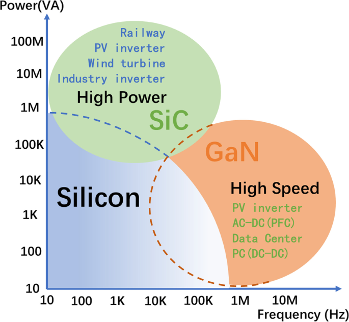
GaN和SiC功率开关晶体管的潜在应用[7]
作为最成熟的宽禁带半导体,SiC 器件在过去十年取得了显着进步,并在高电压、低比导通电阻和快速开关速度方面表现出良好的性能 [8]。鉴于自 1980 年以来的深厚研究基础和可用的低缺陷 (<10 4 cm −2 )、SiC SBD 和结型场效应晶体管 (JFET) 是自 2001 年以来第一个商业化的基于 SiC 的器件。性能 [9]。
与 SiC 相比,GaN 器件的发展非常缓慢。它们不令人满意的材料质量阻碍了它们某些理论上优越的特性的实现。由于缺乏 GaN 衬底,现阶段对 GaN 器件的大多数研究主要基于横向结构(例如,AlGaN/GaN 异质结构)。具有 2000 cm 2 的更高电子迁移率 /V s(AlGaN/GaN 中的二维电子气 (2DEG)),1000 cm 2 /V s (bulk GaN) 和更高的饱和速度 2.5 × 10 7 cm/s 相对于 SiC 对应物,AlGaN/GaN 器件更适用于高频应用,并且相对于 SiC 器件具有低功率瓦特 [10]。在高频领域,AlGaN/GaN SBD 获得了优异的电传输性能,更适合瓦特级的微波和毫米波应用 [11, 12]。 AlGaN/GaN SBD 是 GaN SBD 的代表性器件。 2DEG 的高迁移率意味着 AlGaN/GaN SBD 在高频应用中表现出相对于垂直 SBD 的巨大性能优势,并且还保持低导通电压。最近,AlGaN/GaN SBD 成为 5.8 GHz 整流器电路的基础,其输入功率为 6.4 W,开启电压为 0.38 V,击穿电压 (BV ) 3000 V [13, 14]。最大截止频率在 0 V 时接近 1 THz,阳极到阴极距离为 70 nm [15]。
对于基于 GaN 的功率器件,GaN 衬底(块体 GaN)是外延生长的理想选择,可以利用同质外延技术消除失配。体 GaN 的低位错密度对于外延衬底至关重要,因为高位错密度会影响性能特性,例如 BV 、反向漏电流、生产量和可靠性[16]。近年来,GaN衬底的进步推动了垂直GaN基器件的发展。但鉴于垂直三极管技术相对不成熟,垂直氮化镓二极管成为现阶段的热门研究课题。与AlGaN/GaN SBD相比,垂直GaN SBD在频率领域具有相似的优势,例如高开关速度、低反向恢复时间和低传导损耗;然而,后者电流密度大,泄漏路径比前者少[17, 18]。
GaN衬底出现了一些问题。首先,目前可用的 GaN 衬底的位错密度为 10 4 –10 6 cm −2 ,但这些位错密度仍远高于 Si 和 SiC 衬底 [19]。其次,关于4-6英寸晶圆尺寸和合理成本(10欧元/厘米 2 ) 的 SiC,2-3 英寸的尺寸和相对较高的成本 (100 欧元/cm 2 ) 的 GaN 衬底阻碍了 GaN 的大规模商业化和生产力 [20]。除了增加供应商外,异质外延在异质衬底(Si、蓝宝石或SiC)上是降低GaN衬底成本的一种替代方式,但必须解决相对较高的失配和缺陷的挑战。
除了大块材料中的上述问题外,GaN 二极管面临的挑战是实现高质量的 p - 类型的材料。关于形成p的相对先进的技术 通过Al离子注入的-型SiC,未成熟p -型离子注入技术和p的低受体激活 型 GaN 是重要的障碍,它限制了基于 GaN 的器件的结构和制造的发展。因此,提出了不同种类的边缘终端结构来提高GaN二极管的性能,并构成本综述的关键部分。
FS 基板上的垂直 GaN 基器件
直到 10 年前,大多数 GaN 二极管,包括 SBD 和 PND,都是在形成横向或准垂直器件结构的异质衬底上制造的,因为无法获得块状 GaN 衬底。横向或准垂直二极管显示出出色的电气特性,但它们仍然存在器件结构的固有缺陷 [21]。首先,错配和缺陷是不可避免的。然后,对于异质衬底上的 GaN 器件,GaN 漂移层和异质衬底之间的缓冲是必不可少的。因此,缓冲层的应力松弛会导致晶片弯曲,从而降低 GaN 外延层的厚度 [22]。此外,大的热边界电阻(带衬底的GaN)对高功率密度下工作的GaN器件的性能有严重影响[23]。
随着外延技术的发展,用于垂直GaN器件的低位错密度的自支撑GaN(FS-GaN)衬底取得了长足的进步。 FS-GaN衬底上的同质外延GaN材料质量有明显改善,显示出电源应用的潜力。垂直 GaN 器件可以减轻横向 GaN 对应物的缺点。首先,可以在没有任何缓冲的情况下生长更厚的 GaN 外延层,以及更高的 BV (超过横向GaN器件的)可以由漂移层的厚度获得和确定。同时,最大电场位于器件内部且远离器件表面(消除了通常发生在横向器件中的电子俘获效应)。鉴于 FS-GaN 衬底的高质量,自 2011 年以来一直在研究垂直 GaN 器件 [24]。从那时起,具有高 BV 的垂直 GaN PND 和低导通电阻已经被制造出来并取得了显着的性能。
PND 与 SBD
对于实际应用,二极管是功率转换和逆变的重要组件 [25]。凭借GaN独特的材料特性,GaN基二极管(SBD和PND)表现出显着的性能,有望满足电源应用的要求。如图 2 所示,PND 在结构各异、耐压 600~5000V 的 GaN 器件中应用范围最大,应用场景更广。
<图片>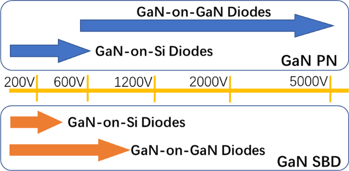
近年来报道的主要垂直GaN功率器件的器件类型、报道和电压等级概述[26]
与没有少数载流子存储问题和较低 SBD 势垒高度的 PND 相比,GaN SBD 具有较低的正向开启电压 (V on) 和快速反向恢复,这些特性表明 SBD 的优点体现在低导通/开关损耗、高频操作,但 BV 价值高于PND;此外,请注意高开启电压会导致高传导损耗并降低电路和系统的效率[27, 28]。
在高功率领域,准垂直或垂直 SBD 与 AlGaN/GaN SBD 相比具有出色的优势 [29]。此外,通过使用低功函数金属调整势垒高度,可以实现低开启电压 (<0.5 V)。然而,较低的势垒高度容易导致较高的反向漏电流并降低BV .因此,提出了各种边缘终止结构以提高性能。通过各种边缘终止技术 [27, 28, 30, 31] 的帮助,KA/cm 2 下的高电流密度 BV 评分 s 超过 1 kV 得到确认。同时,垂直 SBD 还表现出强大的高频能力,例如 177-183 GHz 和 0 V 时的最大 902 GHz 截止频率,这是太赫兹无线通信系统中的电源所期望的特性 [12, 32]。
关于 n -型 GaN,p 通过使用 Mg 作为受体引入了通过金属有机化学气相沉积 (MOCVD) 和分子束外延 (MBE) 生长的 型 GaN [33]。与 GaN SBD 相比,GaN PND 具有许多优点,例如比导通电阻 (R 在A ) 以及足够的器件稳定性和抑制浪涌电流的能力。尽管具有高导通电压 (> 3 V) 和相对较低的开关速度,但由于更高的势垒高度和高 BV 导致的超低漏电流 获得。请注意,较高的 BV 从 0.6 到 5 kV 是基于 GaN 的 PND 的最出色的性能。因此,基于 GaN 的 PND 作为下一代高功率应用的重要构建模块具有巨大的潜力,这些应用需要高效率和低能量损失 [34]。与垂直 GaN SBD 类似,还制造了 GaN PND 的边缘终端,以减轻阳极周围的电场拥挤,本文稍后将详细描述这一特征。
在功率器件中,PN结也可以看作是一种新型的结结构。利用高BV 同时具有PND的低反向漏电流、高开关性能和低开启电压的SBD,包括结势垒肖特基(JBS)和合并PN肖特基(MPS)在内的新型器件结构产生了SBD和PND的组合p的形成 肖特基接触区中的 型网格区。 JBS 或 MPS 器件具有 SBD 正向传导和 PND 反向阻断的特性,有望分别比传统 PND 和 SBD 具有更好的开关性能和更高的反向电压[35]。
除了高功率应用之外,GaN PND 还被用于光电器件,例如发光二极管 (LED)、光电探测器和火焰传感,因为 GaN 基 PN 结光电二极管中的暗电流只有几 pA [36] , 37]。
本评论的目的
基于GaN优异的材料特性,GaN基器件作为最热门的半导体材料之一,得到了广泛的研究并在电力电子应用中得到了应用。在基于 GaN 的器件中,垂直 GaN 基 PND 已被大量探索并显示出出色的 BFOM。边缘端子技术对于缓解阳极焊盘周围的电场拥挤也是必不可少的。
在这篇综述中,以材料外延生长和边缘终端技术的进步为主要重点,接着说明了当前的 GaN 发展、GaN SBD 和 PND 在机制和特性方面的差异,以及垂直器件相对于横向器件的优势.这篇综述提供了一个展望并揭示了用于电源系统的垂直 GaN PND 的设计趋势,包括早期的垂直 GaN PND。对应于垂直 GaN PND 中不同层的外延生长的发展在第 3 节中介绍。 2. 边缘终端技术探索。 3.在宗派。在图 4 中,展示了硅衬底上的垂直 GaN PND 作为替代方法。最后给出了垂直GaN PNDs未来发展的结论和展望。
材料外延生长
垂直 PND 的 GaN 衬底
作为主流的外延工艺,垂直器件外延层目前主要通过MOCVD在氢化物气相外延(HVPE)制造的导电GaN衬底上生长。在这种结构中,衬底的质量直接影响后面的外延结构。器件中的许多故障机制源于衬底外延质量 [38]。必须获得高质量的导电GaN衬底以进一步提高正向和反向I –V 性能,尤其是反向漏电流和BV 能力。
HVPE 生长的基板因其相对较低的成本和可重复性而被认为是最方便的大规模生产方法。然而,早期的生长技术不成熟意味着HVPE生长的GaN衬底具有较高的背景载流子浓度(> 10 19 厘米 −3 ) 和不满意的晶体质量。因此,不采用 HVPE 来生长器件结构 [39]。随着外延生长技术的快速发展,HVPE 制备高质量块状 GaN 材料逐渐成为可能[40, 41]。除了衬底之外,器件中的部分外延层现在可以通过 HVPE 生长,并且通过将 HVPE 和 MOCVD 外延工艺与无碳技术相结合,可以产生更高的电流均匀性并消除 GaN 表面上的宏观台阶。完全通过 MOCVD [42]。
目前,最小位错密度小于10 4 的商用GaN衬底 cm −2 可用。处理了低缺陷密度 GaN 衬底上的 GaN 垂直 PND。然而,晶片弯曲仍然是一个问题。作为一种有前景的解决方案,氨热法可以获得具有更好外延质量的GaN衬底。采用高压釜和超临界氨,穿线位错可显着降低至10 4 –10 5 cm −2 [43]。使用氨热法,0.001Ωcm 2 的低电阻 在具有高掺杂 n 的 GaN 衬底中 -type (1 × 10 19 –1 × 10 20 厘米 −3 ) 以及 BV 3 kV [44]。然而,氨热法的缺点是生长速度低,约为 80-90 微米/天,这对实际生产不利。提高生长速度和保持较高的材料质量也是后续研究的盈利方向。
除了商用 GaN 衬底外,还研究了一些衬底的独特性能,包括非 Ga 面 (c -平面)基板。通常,Ga 极(即 c -平面)衬底用于 GaN 垂直器件。然后,以下外延层显示出剧烈的极化效应。然而,在 Ga 极性对应物的相反方向上,沿 N 的同质外延层 -polar 方向显示出独特的器件特性,因为它具有更高的分解温度和极性相关特性 [45, 46]。随着 N -极性单晶 FS-GaN 衬底,实现了 2.2 MV/cm 的电场,没有任何边缘终止,以及 BV 2.4 kV,采用 N2O 表面等离子体处理和场板 (FP) [46, 47]。作为另一种特殊的 GaN 衬底,m -plane 也因其非极性特性而引起广泛关注,其中 Ga:N 在 m 中为 1:1 -平面仅相对于 c 中的 Ga -polar 并且只有 N 在 N -极性底物。使用这种非极性 GaN 衬底,PND 的特性被报告为具有 2.0 MV/cm 的临界电场和高开/关比,没有 FP 或边缘终止 [48]。
N-GaN 外延技术
在高质量导电 GaN 衬底出现之前,GaN PND 主要制造在外来衬底上,包括 Si、SiC 和蓝宝石。因此,器件的结构总是局限于横向结构。提出了一种基于横向结构的方法来提高外延质量。鉴于横向器件窗口区域上的穿透位错 (TD) 较低,横向生长跨越掩模的 GaN 外延层可以实现低得多的 TD 密度。因此,进行横向外延过度生长以在用于横向 PND 的蓝宝石衬底上生长 GaN 外延层。反向漏电流被抑制了三个数量级[49]。
随着外延技术的发展,低位错密度为3 × 10 –6 的高质量单晶GaN衬底 cm −2 变得可用,并且在 GaN 衬底上制造 GaN PND。结合通过 MOCVD 生长的上外延层,器件表现出低漏电流和高 BV 600 V 至 4 kV,对应于 6 至 40 μm 的漂移厚度 [16, 50]。对于蓝宝石衬底上的器件,反向漏电流和BV 显着改善[51]。
对于原生 GaN 衬底,PND 外延结构中通常不会出现特殊的缓冲层,就像在异质衬底上那样。研究了PND中的缓冲层对GaN衬底的影响作为参考。缓冲层的存在意味着漂移层具有较低的缺陷密度。同时,更高的BV 可以用更薄的漂移层但更厚的缓冲层来获得。器件的反向漏电流也得到改善。这些器件参数与缓冲层的厚度有很强的相关性,对器件的正向特性有轻微影响[52]。
如本部分所述,上外延层通过 MOCVD、金属有机气相外延 (MOVPE) 和 MBE 沉积。 PNDs的外延结构包括一个高度掺杂的n + -GaN层和n的漂移层 - -衬底和p之间的GaN -GaN(图 3)。高掺杂 n + -GaN层在一些报道中作为导电GaN衬底上的过渡层。
<图片>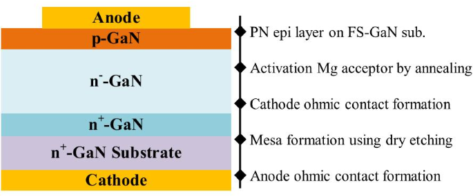
GaN垂直PND结构示意图
一般来说,BV 决定了设备的应用场景。例如,较高的 BV SiC 器件相对于 GaN 器件的差异允许 SiC 器件用于电动汽车和子弹头列车等高功率和高电压应用(图 1)。类似地,相对于肖特基二极管和 HEMT,PN 二极管通常应用于更高的电压。在 PND 中,BV 主要由漂移层(轻掺杂n - -GaN 层),耗尽区变宽(如方程 1 所示,施加电压 V 其中 V 当器件处于反向偏置时,正向/反向偏置为正/负。而且,随着反向偏压的进一步增加,击穿发生。
$${W_{\text{D}}} =\sqrt {\frac{{2{\varepsilon_{\text{s}}}\left( {{V_{{\text{bi}}}} - V } \right)}}{q}\frac{{{N_{\text{A}}} + {N_{\text{D}}}}}{{{N_{\text{A}}}{N_ {\text{D}}}}}}}$$ (1)其中 S , q , V 双, N D 和 N A分别为结面积、电子电荷、内建电位、施主浓度和受主浓度[53]。
根据耗尽宽度,器件可分为非穿通[W D> W Dm (W Dm:最大耗尽层宽度)]和穿通(W D <W 米)。鉴于外延结构和边缘问题,大多数 GaN 垂直器件属于穿通型,即它们的耗尽区扩展到整个 n - -GaN层并达到n + -击穿前的GaN衬底。
此外,如方程中所述。 (2)、BV 可以通过增加厚度和减少 n 来增强 -型漂移层掺杂浓度。
$${\text{BV}} ={E_{\text{C}}}t - \frac{{q{N_{\text{D}}}{t^2}}}{{2{\varepsilon_0 }{\varepsilon_{\text{r}}}}}$$ (2)其中 E C、q , t , N D 和 ε r 是临界电场,电子电荷,n - -GaN层厚度,n的净载流子浓度 - -GaN 层和半导体介电常数,分别为 [54]。幸运的是,经验表明,厚度较厚、掺杂较低的漂移层仅对正向传导的导通电阻略有增加。
与增强BV相比 通过增加漂移层厚度,降低 n n 中的 -type 掺杂浓度 - -GaN层目前是困难的,因为包括Si、O等的背景浓度高。为了进一步降低 n 中的掺杂浓度 - -GaN 层,研究了无意的掺杂浓度。许多研究小组推出了标称 i-GaN 大约 10 15 –10 16 cm − 3 联系p -GaN形成p –i –n 提高二极管BV的结构[55]。
当然,这些措施的前提是漂移层的高外延质量,因为TD会增加断态泄漏并降低BV 属性 [56]。
为了进一步提高 GaN 垂直 PND 中漂移层的外延质量,研究了 MBE 在 GaN 衬底上的生长。漏电流小于 3 nA/cm 2 通过非常低的位错密度获得 3.1 MV/cm 的电场。近乎理想的击穿性能表明 MBE 是一种在 GaN 垂直 PND 中生长外延层的有效方法 [56]。然而,与氨热生长类似,外延速率是另一个缺点。
P-GaN 外延
P-GaN 是 GaN 垂直 PND 的重要组成部分,自 1969 年 HVPE 出现 GaN 以来,于 1989 年被报道 [57, 58]。它首先被用来获得蓝色 LED。然后,p -GaN逐渐应用于常关器件和PND等电子器件领域。在垂直 GaN PND 中,p -GaN 构成光(大约 10 19 厘米 −3 ) 和重 (≥ 10 20 厘米 −3 )掺杂浓度,对应于与漂移层形成PN结层,促进欧姆接触作为阳极。
通常,p 的外延生长 -GaN 是通过 MOCVD 在大约 1000°C 的温度下制造的,并采用 Mg 2+ 作为接受者。然后,成长的p -GaN 层必须在 N2 环境中 700-800°C 或 O2 环境中 400°C 的高温下激活,从而促进相对较高的空穴浓度 [59,60,61]。然而,Mg-H 键的 150-200 meV 高电离能意味着 p -GaN 激活率仅为 1-3%。低活化率也与温度有关。在 NH3 或氢气环境中,Mg 掺杂剂可以在≥ 600°C 的高温下重新钝化 [62]。为了提高空穴浓度,单独提高掺杂浓度是不可行的,因为 p 中的掺杂浓度更高 -GaN 可能会导致层的结晶质量恶化,并通过自补偿效应降低空穴密度 [63]。目前,空穴密度的峰值通常可以在大约3 × 10 19 的受体浓度下达到 厘米 −3 [64]。虽然对于 p 有一些问题 -GaN,相关调查报道不多。这可能归因于两个原因。一是材料和外延设备固有特性的局限性。另一个是现在的 p -GaN 也可以获得比较器件的性能。
然而,生长条件的优化和新的外延工艺仍在研究中。例如,在 2017 年,未激活的再生p 由 MBE 提出的 -GaN 比 MOCVD 具有优势。在低氢生长环境下,BV 通过制造的垂直 GaN PND [65] 实现了 1.1 kV 和 2.5 的理想因子。另一个有趣的p -GaN 制造方法是采用超高压退火 (UHPA) 工艺的 Mg 离子注入。结果表明,70% 的高激活率和 24.1 cm 2 的空穴迁移率 V −1 s −1 通过在 1573-1753 K 的温度和 1 GPa 的 N2 压力下进行植入后退火来实现。该结果与MOCVD外延生长的结果相当[66]。
总之,对于衬底,现在可以使用商业化的低缺陷 GaN 衬底。同时,外延技术仍在发展中,这种情况对器件性能有很大影响。与 MOCVD 相比,MBE 可以实现出色的外延质量,从而在没有任何边缘终端的情况下实现出色的器件性能。然而,其缓慢的增长速度和高成本使得 MBE 不适合大规模生产。 MOCVD外延生长仍然是实际生产中的主要生产方法。因此,提高通过 MOCVD 生长的外延层的质量是一个紧迫的问题,这需要相当长的时间。因此,现阶段提出了先进的器件结构设计或措施以实现良好的性能。
边缘终止技术
对于垂直 GaN PND,BV 是一个重要参数。 Almost all investigations on vertical GaN PNDs are centered on improving the withstanding voltage at reverse (i.e., BV )。 However, due to the electric field crowding at the edge of PN junction, the depletion layer edge, or the electrode edge, premature breakdown often occurs. Therefore, to reduce the electric field crowding of the device, advanced device structure designs (i.e., edge termination techniques) are developed. Varied edge termination techniques have now been adopted to relax the electric field crowding at the edge of GaN PNDs for a higher BV . These techniques include mainly the field plate (FP), ion implantation and plasma treatment, and mesa etching in varied angle or steps and guard rings (GRs) [49, 67,68,69]. These features are discussed in this section.
Metal Field Plates
The FP has been widely utilized in GaN-based devices for transferring the peak electric field far from the edge of the gate, anode, or junction. This method has an identical feature to relax the intensity of the electric field at the PN edge under reverse bias. Moreover, the low leakage current and high breakdown voltage under reverse voltage can be achieved by using FP termination, which has a relatively simple fabricating process as well.
The merits of the FP structure include a simple fabrication process and compatibility with the device process. Simultaneously, the dielectric layer of FP is also the passivation layer of the device. As the earliest and most widely used edge termination for vertical GaN PNDs, the non-extended FP termination was initially used, as shown in Fig. 4a. For fabricating the FP structure, mesa structures were processed by inductively coupled plasma (ICP) dry etching. Then, to suppress the parasitic leakage currents from plasma damage, a passivation dielectric film was deposited all over the anode electrode and the entire mesa structure [70].

PNDs’ structures with a FP and extended passivation dielectric layer and b extended FP metal and passivation dielectric layer [70, 71]
To furtherly relax the electric field crowding at the periphery of the PN junction edge, the extended metal of the FP was utilized to cover the entire mesa to reduce the reverse leakage current and raise the BV [71]. This optimized FP structure is now widely employed in vertical GaN PNDs fabrications. As shown in Fig. 4b, the BV was raised over 3 kV with an extended FP structure. Meanwhile, the reverse leakage current was also suppressed to a quite low level at revere voltage of 3 kV.
As an essential component of the FP structure, the passivation layer has a considerable impact on the device characteristics. Thus, an appropriated passivation layer is essential. A passivation layer owned high-k permittivity is proposed by simulation, and uniform reverse current flow can be also obtained [50]. According to this theory, vertical GaN PNDs with FP termination using Ga2O3 (the dielectric permittivity of 10) as passivation film were reported. The BV had a large improvement from 200 to 550 V, thereby revealing that a high-k permittivity film such as Ga2O3 is promising as a passivation film of FP termination in vertical GaN PNDs for raising device characteristics [72]. However, some demerits arise for FP termination. The main issue is the defect during the dielectric layer deposition and interface between the dielectric and GaN, which result in carrier trapping. These would lead to the instability of device performance during long-term use. Therefore, the optimized deposition process of the dielectric layer must be investigated.
Mesa Termination
Mesa etching is an indispensable step to isolate adjacent devices in the fabrication of planar GaN-based devices. Given the simple process, this structure is popular for vertical GaN PND processes. Aside from a uniform electric field at the edge of PN junction, a high BV with nondestructive and avalanche characteristics can be achieved in PNDs. For instance, a simple but deep mesa structure can obtain great performance. As shown in Fig. 5a, with more than 10 µm depth of mesa structure in vertical PNDs, nondestructive BV and avalanche characteristics were confirmed [73].

一 PNDs with deeply etched mesa structure; b PNDs with two-step mesa [73, 74]
The novel mesa structures are investigated as shown in Fig. 5b. A multi-mesa (two-mesa) structure was adopted in vertical PNDs. With respect to the common single mesa structure, the two-mesa structure can shift the peak electric field from the edge of the PN junction to underneath the thinned p -GaN in the upper mesa because of the total depletion of holes in the thinned p -GaN layer. A high BV of 4.7–4.8 kV with nondestructive feature was successfully achieved by the two-mesa structure. Avalanche capability was obtained without lowering the forward I –V characteristics [74]. On the other hand, the two-mesa structure has the identical function for quasi-vertical PINDs [75]. The BV was enhanced from 665 to 835 V with the low leakage current simultaneously.
Besides the common perpendicular mesa structure, a mesa structure with negative bevel was recently proposed to mitigate the electric field crowding at edge of the PN junction. With the negative bevel mesa, the electric field at the edge has a decreasing trend when the bevel angle θ is lowered from 90˚. The peak electric field would be transferred into device inner. In [76], experimental investigation showed that beveled mesa structure (Fig. 6a) could induce a higher BV over 3 kV and a low leakage current with respect to BV of 3 kV in PNDs with steep mesa when using the same FP structure. Further investigation was performed by simulation using technology computer-aided design (TCAD). In vertical GaN PNDs with beveled mesa (Fig. 6b), the maximum electric field was determined by the acceptor concentration N A in p -GaN, donor concentration N D in n - -GaN drift layer, and θ of the beveled mesa. By theoretical analysis and simulation, the smaller θ could lead to higher E pp (parallel-plane breakdown field). At the same time, a lightly doped p -GaN is beneficial for achieving high BV for a fixed θ of the beveled mesa. Taking θ = 10° as an example, the experimental results support these findings. A parallel-plane breakdown field of 2.86 MV/cm was achieved, and this outcome is consistent with the simulation [77].

Schematic cross of PND structure with a bevel mesa and FP structure, b PND epitaxial structure is simulated by treating N A, N D and θ as variable [76, 77]
Similar with FP termination, the dry etching and/or insulator (or passivation film) is required in process of edge termination. Thus, the damage from dry etching must be considered and can cause a high reverse leakage current, even the premature breakdown. At the same time, it is a high demand to etched equipment for etched precision, and the etched depth is difficult to control. Meanwhile, the existence of damage generates a more complicated interface state between the insulator and the etched semiconductor, a situation that would affect device reliability. Consequently, reducing or alleviating damage is an inevitable issue. Now, some recipes (e.g., tetramethylammonium hydroxide (TMAH) and post-annealing that have the features of removing the damage by wet etching and repairing dry etching damage, respectively) have been adopted to treat etched surface to improve performance.
Ion Treatment
Ion implantation was employed to alleviate the electric field concentration near the edge. As a relatively simple termination structure, an implantation-based technique was investigated in GaN devices, which includes the compensating species (e.g., O, H, and Zn) or inert species (e.g., Ar, N, He, and Kr) to create deep-level traps in the termination regions [78,79,80,81,82]. Recently, for moderating the occurring of premature breakdown in vertical GaN PNDs, the ion implanted termination (e.g., N, F, Mg, and H) is also utilized. However, the mechanisms of these ion implanted terminations are different.
With respect to vertical GaN SBDs [83], N implantation in vertical GaN PNDs reveals a different mechanism, which entails creating the donor-like defects (N vacancy and N interstitial) to compensate for the p -type dopants. After processing by N implantation as shown in Fig. 7a and b, the conductivity of p -GaN can be reduced or eliminated (insulating) by N implantation [53]. To further improve the BV , a non-fully compensated layer was proposed, that is, a fully compensated layer coupled with a partially compensated counterpart in p -GaN. Thus, a higher BV was expected, and the mechanism was analyzed by simulation [84]. The experimental results show that N implantation with partially compensated p + -GaN could induce a BV of 1.68 kV without compromising the forward characteristics [85].

一 Cross-sectional plot of the PNDs with N implantation termination, and b N implantation termination with fully and partially compensated [53, 84]
The hydrogen-plasma (H-plasma) edge termination can also reduce p -GaN conductivity, but with another mechanism. H-plasma treatment is an effective passivation method to transform the conductive p -GaN into a highly resistive one because of the strong bond of Mg-H in p -GaN. In contrast to N implantation, the H-plasma treatment is more appropriate for use in vertical GaN PNDs because of the low damage, low temperature, and simple operation involved. As shown in Fig. 8a, the PNDs exhibited an electric field of 3.0 MV/cm with just the H-plasma treatment. Simultaneously, the devices showed comparable forward I –V characteristics and a lower reverse leakage current [86].

一 Schematic view of PND structure by Mg ion treatment; b PNDs with H2 plasma treatment [86, 88]
At the same time, fluorine (F) ion also has the capability of modulating the peak electric field due to the negative fixed charges when the device is under a reverse bias. Nevertheless, if the F implanted edge termination is carried out in vertical GaN PINDs, strict design and structural optimization are needed [87].
In addition to the N, H, and F ion implantation as edge terminations, Mg ion implantation is also an alternative method to convert the surface/interface state, which originates from the damage of ICP dry etching. A novel Mg ion implantation coupled with moat mesa was recently adopted to compensate for the donor-like damage for GaN vertical PNDs (Fig. 8b). Then, a BV of 1.5 kV was achieved with a specific on-state R on of 0.7 mΩ cm 2 [88].
Ion implantation termination is an effective method for a high BV in vertical GaN PNDs. The ion implantation process is also relatively simple. However, crystal damage occurs during high-energy ion implantation. Moreover, post-annealing at high temperature is required in some of the ion implantation terminations for alleviating the crystal damage. The rectangle-shaped ion implantation profile is pursued, so the implantation depth must be controlled exactly. Finally, although the ion implantation process is simple, the equipment needed is costly due to usage of high energy ion.
Guard Rings
The use of floating guard rings (GR) as edge termination to improve BV is an effective method for vertical GaN PNDs, for which the reverse voltage has a voltage drop over the GR to relax the electric field crowding. At the same time, the GR fabrication process does not require a specialized step, which is synchronous with anode metal deposition. For a higher BV , a GR in the FP structure was fabricated in the PNDs (Fig. 9a), in which polyimide was set between the GR and anode portion as resistive device for a further voltage drop. Due to the resistance portion, an incremental 0.2–0.4 kV of BV to a maximum of 5.0 kV was obtained. Compared with normal PNDs without a GR structure, the device with a resistive GR exhibited a similar forward I –V characteristics with R on of 1.25 mΩ cm 2 , but a lower reverse leakage current with BFOM of 20 GW/cm 2 [69].

一 Vertical GaN PNDs structure with floating GR termination; b PNDs structure with H-implanted GRs [69, 90]
Besides the floating GR, the H-plasma-based GR structure was also applied to form the edge termination. In addition to low damage, the low diffusivity of H-plasma could result in relatively ideal profile in GaN [89]. Owing to passivation effect of the H-plasma on p -GaN, the conductive p -GaN becomes highly resistive, and the GR structure was subsequently formed by the highly resistive p -GaN ring (Fig. 9b). The narrow GR width of 1–2 µm and decreasing spacing were used to improve the BV. GR structures with varied rings were measured. The PNDs with varied rings have similar forward characteristics with around 0.65 mΩ cm 2 and an ideality factor of 1.65 compared with those without GR. More GRs could further relax the electric field at the device edge. Thus, the devices exhibited a higher BV by increasing the number of rings after measurement. Consequently, the PNDs showed a BV of 1.7 kV with the highest electric field of 3.43 MV/cm 10 GRs [90].
The disadvantage of GR is its low area utilization rate, and the GR structure generally requires a large area, which is even bigger than anode. Then, the amount of GR raises the design difficulty such as the width and spacing of the GR. At present, two and more kinds of edge termination are adopted in single vertical GaN PNDs for a higher BV . These edge terminations typically include the FP, bevel mesa, and guard rings due to the relatively simple fabrications. On the other hand, these edge terminations are not meant to introduce the foreign element into the GaN crystal with respect to ion treatment, a feature that is beneficial for device performance. However, the quality of epitaxial layers still occupies a considerable proportion.
Vertical GaN PNDs on Si Substrate
To date, although vertical GaN-on-GaN devices exhibit excellent performance, the high cost and small diameter of GaN substrates still impede their large-scale market applications. Consider to the merit of a large scale and low cost of Si substrate, GaN-on-Si devices have attracted considerable many attentions at this stage.
For the quasi-vertical PND on Si substrate, high-quality buffer is essential. In [91], as shown in Fig. 10a, optimizing the AlN nucleation layer and the succeeding growth process, a GaN drift layer with a low threading dislocation density of 2.95 × 10 8 cm −2 and high electron mobility of 720 cm 2 /Vs was obtained. With the FP structure, the device has a BV of 820 V with R on of 0.33 mΩ cm 2 .

一 Quasi-vertical PINDs with FP; b fully vertical PNDs by using the thin AlN and SLS superlattice structure on conductive Si substrate; c PNDs with trenched ohmic contact on back; d PNDs fabricated by layer transfer technology [91,92,93,94]
In addition to the challenge of materials mismatch, the conductive buffer layer and Si substrate are fundamental for fully vertical PNDs on Si substrate. In Fig. 10b, a n + -type Si substrate was first utilized as the cathode of vertical PNDs. Subsequently, the Si-doped thin AlN layer and GaN/AlN strained superlattice layer were employed to facilitate device performance [92]. Vertical PNDs on Si substrate are proposed with FP, and a BV of 288 V is confirmed with a drift layer of 1.5 µm. Moreover, a higher BV of 720 V in PNDs on Si with 5.7 µm drift layer is reported in Fig. 10c [93]. Unlike the conductive Si substrate method, the cathode ohmic on back approach was made by a trench, which reaches the n + -GaN layer through the selective removal of regular Si substrate and buffer layer.
Besides the conductive Si substrate and trenched ohmic contact on back, substrate removal technology is an alternative method to produce vertical GaN PNDs on Si substrates. In Fig. 10d, a layer transfer technology is used to process vertical PINDs on Si substrate. After Si substrate removal, transfer, n -electrode, and sidewall passivation, the devices exhibit a low R on of 3.3 mΩ cm 2 and BV of 350 V [94]. The high BFOM value of 37.0 MV/cm 2 in PINDs demonstrates that substrate removal technology is an effective way for GaN-based PIND fabrication on Si substrates. Relative to other technologies, however, the more complicated fabrication process and higher production cost are issues that must be addressed during the substrate removal part.
As an alternative technical route, PNDs on Si substrates are fabricated with quasi-vertical or vertical device structures. To mitigate the substantial material mismatch between the Si substrate and GaN epitaxial stacks, a more effective epitaxial technology must be investigated. For a higher BV , thicker drift layer is also essential for a higher BV . This fact presents another key issue to investigate because the drift layer thickness on Si substrate is approximately 5 µm.
Future Challenges and Conclusion
Vertical PNDs are essential to simultaneously obtain high current (> 100 A) with high voltages (> 600 V), which can meet the requirements of several applications including electric vehicles and recycled energy processing. Despite the great progress achieved, applications of vertical GaN PNDs remain several barriers such as cost and technical limitations.
For FS-GaN substrate, high epitaxial quality with low threading dislocation has been achieved by a common MOCVD. The small size and high cost of the FS-GaN substrate confine the applications of the vertical GaN PNDs within a narrow range, and the small size also raises the price of GaN. The commercial GaN substrate is only 2-inch and is much smaller than 4–6 inch SiC and 8–12 inch Si substrates. The primary challenge for vertical GaN PNDs is achieving high epitaxial quality, especially the high quality of the p -GaN layer with a high hole concentration. Recently, novel PNDs are proposed through replacing p -GaN with NiOx synthesized by thermal oxidation or sputtering; great performance is also demonstrated as replacement of p -GaN in vertical PND and guard ring in GaN SBD [95,96,97,98].
Vertical GaN PNDs, as one of the most promising power devices, are reviewed and summarized in this study. The recent progresses on vertical GaN PNDs, including comparison of different materials (SiC vs. GaN) and different device structures (SBD versus PND), material epitaxy growth and edge termination techniques (FP, MESA, ion implanted and GR edge terminations), are discussed. R 的值 on versus BV by varied technologies are plotted in Fig. 11. Aside from the epitaxial technologies, edge termination technologies play a key role for vertical GaN PNDs to achieve high device performance at this stage. Despite its great progress in terms of device performance, the advantages of vertical GaN PNDs remain under-exploited. The characteristics of vertical GaN PNDs could be promoted by optimizing the device structure and epitaxial quality in succeeding studies. Then, commercialized vertical GaN PNDs will soon be available in the future with mature edge termination and epitaxial techniques.

Benchmarking of the R on versus BV of quasi- or full-vertical GaN PNDs
数据和材料的可用性
The datasets used or analyzed during the current study are available from the corresponding author on reasonable request.
缩写
- GaN:
-
gallium nitride
- 碳化硅:
-
silicon carbon
- PND:
-
PN junction diode
- PIND:
-
P-i-N junction diode
- SBD:
-
肖特基势垒二极管
- IGBT:
-
insulated gate bipolar transistors
- BJT:
-
bipolar junction transistor
- MOSFET:
-
metal oxide semiconductor field effect transistor
- BFOM:
-
巴利加的功绩
- HFET:
-
heterostructure field-effect transistor
- JFET:
-
junction field-effect transistor
- 2DEG:
-
two-dimensional electron gas
- BV:
-
breakdown voltage
- FS:
-
free-standing
- MOCVD:
-
metalorganic chemical vapor deposition
- MBE:
-
molecular beam epitaxy
- JBS:
-
junction barrier Schottky
- MPS:
-
merged PN Schottky
- LED:
-
light-emitting diode
- HVPE:
-
hydride vapor phase epitaxy
- FP:
-
field plate
- TD:
-
threading dislocation
- MOVPE:
-
metalorganic vapor phase epitaxy
- HEMT:
-
high electron mobility transistor
- UHPA:
-
ultra-high-pressure annealing
- GR:
-
guard ring
- ICP:
-
inductively coupled plasma
- TCAD:
-
technology computer-aided design
- TMAH:
-
tetramethylammonium hydroxide
纳米材料