

最全面的印刷电路板组装指南
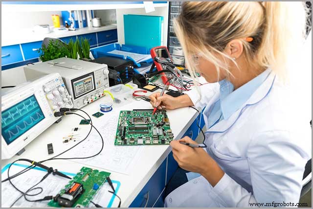
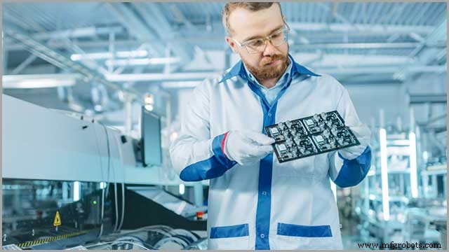
什么是印刷电路板组件?
也称为 PCBA,印刷电路板组装可能是一个非常复杂的概念,难以理解。但是为什么,你可能会问。原因是PCBA与印刷电路制造不同,也称为PCB。印刷电路板组装和PCB制造是两个不同的学科,具有不同的要求和标准。
正确的 PCB 服务提供商。值得庆幸的是,有各种PCB制造都是关于电路板的制造。另一方面,印刷电路板组装涉及在已制造的板上制造或放置组件或零件。
PCB组装前的准备工作
印刷电路板是电子产品中的一个关键概念。可悲的是,很多人不了解印刷电路板的重要性。更糟糕的是,很多人在PCB组装之前并不了解成分和准备工作。以下是您在SMT之前需要了解的内容)。这将使拾取和放置机器轻松地在PCB(PCB组件)上轻松拾取和放置组件。
2.1 PCB设计基础
基板 – PCB 基板是固定 PCB 组件和走线的固体材料。在 PCB 组装之前,您需要确保使用正确的基板材料。选择正确的基板是获得最佳 PCB 的第一步。简而言之,正确的基板材料主要影响您的 PCB 性能。
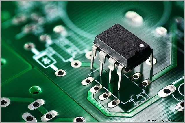
铜——铜是制作走线最常用的元素之一。但为什么铜是整个印刷电路板行业的时尚选择?铜最显着的好处是它具有高导电性。铜可以正常传输信号而不会在途中损失电力。
阻焊层——阻焊层是位于铜箔顶部的一层。该层使印刷电路板呈现绿色。阻焊层覆盖在铜层上以绝缘铜迹线并保护 PCB 的铜迹线免受氧化。阻焊层还可以防止在紧密间隔的焊盘之间形成焊桥。
2.2 PCB组装需要电子零件和耗材
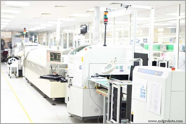
印刷电路板的构造不同于制造电路板。印刷电路板的生产涉及多个过程,例如设计和创建 PCB 原型。印刷电路板组件需要一些东西。以下是 SMT 所需的电子零件和消耗品)。这将使拾取和放置机器轻松拾取和放置 PCB 上的组件(PCB 组装:
印刷电路板
电子元件
焊接烟道
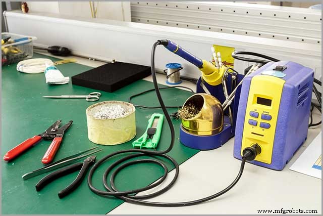
焊接设备
(波峰焊机、焊台、SMT设备、检验和测试设备)。
2.3 PCB的三种主要类型
印刷电路板主要根据频率、使用的基板和比率进行分类。一些最受欢迎的包括以下内容:
• 刚性PCB – 刚性PCB 是由坚固材料制成且不能弯曲的印刷电路板类型。刚性 PCB 结构紧凑,在损坏时非常容易修复。如果您在市场上购买易于维护的 PCB,您最好选择刚性 PCB。
• 柔性PCB – 柔性PCB 由柔性基材组成。这些类型的 PCB 有双面、单面和多层形式。这有助于使装置组装内的复杂性最小化。 WellPCB 在国内和国际市场提供直流电机控制器。我们的柔性 PCB 非常适合密度和温度为主要关注点的工作条件。
• Metalcore PCB:(FR4 板)– FR4 PCB 最近在许多电子设备中得到使用。 FR表示该材料是阻燃的,而4表示用于生产这些类型PCB的四种元素。
2.4PCB组装行业的三大安装技术
• 表面贴装技术——这是一种将印刷电路板的电气元件直接安装在 PCB 表面上的方法。以这种方式安装的电气元件是表面贴装器件(SMD)。
• 通孔技术——这是一种用于电子元件的安装方案,涉及在零件上使用引线,这些引线插入印制电路板上的钻孔中,并手动或自动焊接到委员会对面的焊盘上。
• 混合技术——混合技术也是另一种易于安装的技术,包括使用不同的材料来优化电气性能和提高系统可靠性。
2.5 DFM 检查
什么是 DFM 检查?
也简称为 DFM,制造设计涉及设计零件、产品或组件的过程,以便于制造,从而以更低的成本制造最终产品。 DFM 检查是检查印刷电路板功能的过程。 DFM 检查涉及对材料清单、不推荐用于制造的部件以及需要立即更换的组件的审查。
为什么我们需要进行 DFM 检查?
DFM 检查有很多好处。 DFM 检查使设计人员能够了解产品的再现性和可重复性。它还指导制造过程中的公差以及产品的要求是否合理。 DFI 期间涉及的一些问题包括检查与公差有关的问题将如何影响测量系统并检测与不合格有关的问题。
重要性
如前所述,制造设计是设计产品以使其易于制造的过程。 DFM 是制造新产品之前最关键的制造工具工艺开发和工具设计步骤之一。
在计划设计新产品时,DFM 是必不可少的。说到PCB的制造,DFM是必要的,因为它可以保证产品的生产。使用 DFM,产品不会很快回到绘图板上。其次,DFM 至关重要,因为它会影响产品的感觉、外观、功能和精度。最后,DFM 是必要的,因为它会显着影响您的时间线。
如何进行PCB组装的详细步骤
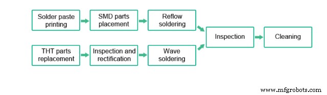
印刷电路板组装本身并不是一个复杂的过程。但是,如果操作不当或匆忙,您最终可能会重复整个过程。没有什么比不得不重复 SMT 更糟糕和更昂贵的了)。这将使拾取和放置机器轻松拾取和放置 PCB 上的组件(PCB 组件。为了安全起见,您可能必须遵循 PCB 快速原型制作的真实步骤。3D PCB 打印不仅制造PCB,但它也负责印刷电路板组装(PCBA,如下所示:
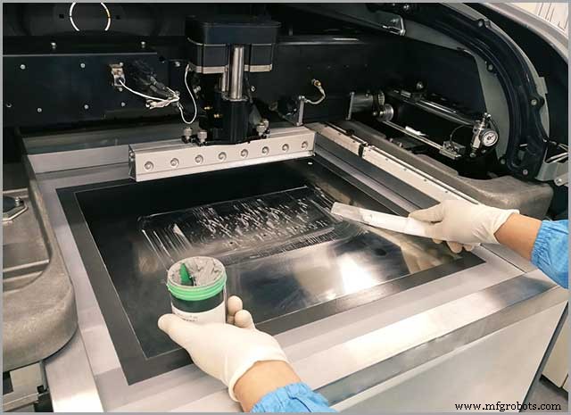
第一步:打印焊膏——当涉及到 PCB 快速原型制作时。 3D PCB印刷不仅制作PCB,还进行印刷电路板组装(PCBA工艺,您需要先将一些焊膏直接涂在板上。该工艺与衣服和服装的丝网印刷相同,从而您在 PCB 上放置一个不锈钢模板。现在它将成为创建新零件的焊膏印刷的基础。
焊料的成分为 3% 的银、95% 的锡和 0.5% 的铜。在 PCB 快速原型设计中。 3D PCB 打印不仅可以制造 PCB,还可以进行印刷电路板组装(PCBA 生产线,机械夹具将焊锡模板和 PCB 完美固定到位。之后,涂抹器会将一些焊膏直接涂抹到该区域意在理想的部分。
第二步:拾取和放置
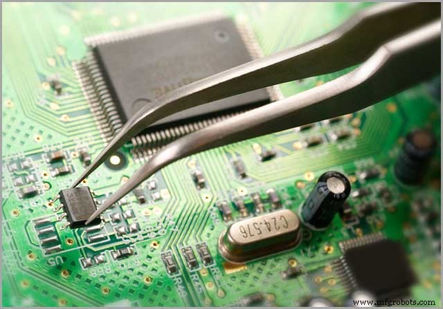
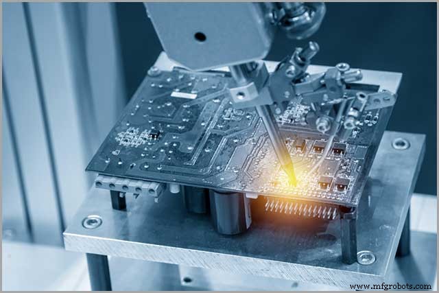
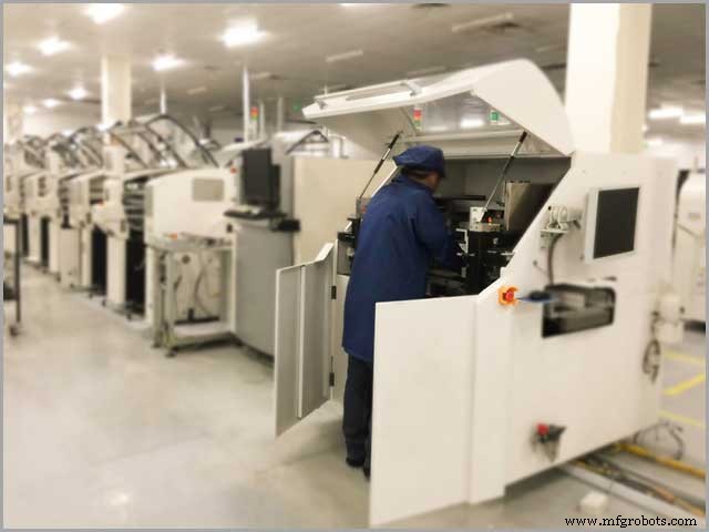
应用焊膏后,PCB 快速成型。 3D PCB 打印不仅可以制造 PCB,还可以进行印刷电路板组装(PCBA 工艺转移到拾取和放置机器。最初,拾取和放置是一种手动方法,您必须使用一对镊子进行组装PCB 的所有元素都是手工完成的。但是,随着技术的进步,现在有机器人可以自动拾取和放置 PCB 的各个部分。机器人还可以适当地定位 PCB 并将表面贴装到 PCB 表面。
第三步:回流焊
PCB 元件和焊膏就位后,它们必须正确粘附。出于这个原因,面团必须凝固才能通过回流将零件连接到板上。大多数PCBA在回流过程中需要特别考虑,更多的是双面印刷电路板组装。
第四步:检验与质量控制
当这些元件被焊接到位时,电路板需要进行测试以确定其功能。在回流过程中,移动可能会导致缺少连接或连接不良。 Wne可以手动或自动完成检验和质量控制。尽管智能和自动化制造,您仍然需要在 SMT 方面进行手动检查)。这将使拾取和放置机器可以轻松地在 PCB 上轻松拾取和放置组件(定期进行 PCB 组装。
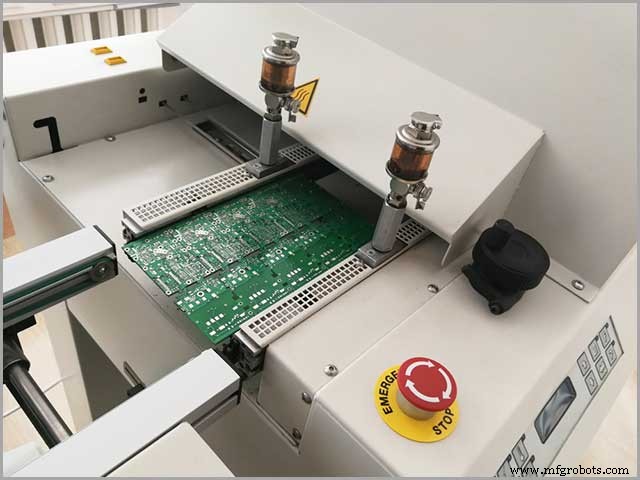
不幸的是,手动组装往往不准确。自动光学检测更适合大批量。在这里,PCB 制造商使用自动化机器在短时间内处理大量 PCB。
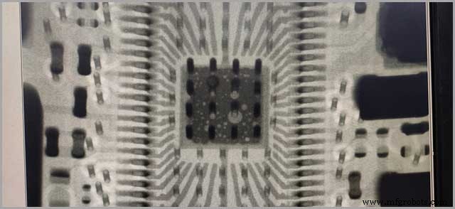
最后,进行 X 射线检查。这种类型的检查方法并不常见,尽管它在复杂和分层的 PCB 中大量使用。使用 X 射线,观察者可以看穿层,然后可视化较低的层以查看隐藏的问题。
第五步:通孔组装
根据正在建造的电路板,它可以承载通常不会出现在表面贴装设备上的各种元件。它们可能包括电镀通孔细节或 PHT。除了焊膏外,PHT 组件可能需要专门的焊接方法,例如手动焊接或波峰焊。手工焊接不是一个复杂的过程。在这里,个人将元素插入指定的 PTH,然后再将它们传输到下一个站点。手动焊接可能是一个非常漫长的过程,许多公司都试图避免使用它。
波峰焊是另一种 PTH 插入方法。大多数人可能将其称为手动焊接的自动化版本,但它完全是一个不同的过程。
第六步:最终检查和功能测试——在完成制造 PCB 所需的生产薄膜工作之后。对于 PCBA,您需要进行最后一次检查以评估 PCB 功能。这项检查使印刷电路板完成了它的步伐,复制了它可能经历的和不太可能发生的情况。测试是必不可少的,因为它决定了 PCB 的成败。如果失败,PCB可以报废或回收。
13 种有效的印刷电路板组装测试方法
如果您正在考虑 PCBA,则需要注意 PCB 故障的高成本。您的愿望清单上的最后一件事是看到您的 PCB 在没有任何警告的情况下掉落。下面介绍13种有效的PCBA测试方法:
4.1 我们为什么要进行 PCBA 测试
PCBA 测试在 PCB 的开发周期中是必不可少的。通过进行测试,WellPCB。我们将为您提供一站式服务和优质产品。您可以将您需要制作的文件发送给我们并立即获得报价!我们还在等什么?我们有十年的 PCB 制造公司可以节省用于返工或回收的资金。通过测试,可以避免不必要的成本。
裸板测试
裸板测试涉及测试裸/空印刷电路板上电子连接的连续性和隔离性。此测试是在连接 IC 等重要部件之前在空白板上进行的。
装配级测试
装配级测试对于检查 PCB 的功能至关重要。这些类型的测试可以手动完成,也可以使用自动化测试设备完成。尽管结果非常好,但机械测试设备往往有点贵。
在线测试
也称为 PCB 的自动化测试,您可以在 PCB 的制造过程完成后进行在线检查。通过在线测试,PCB 使用飞针或适配器 E-Test 设备进行彻底检查。
不带夹具的 FICT 在线测试
无夹具在线测试 (FICT) 的另一个名称是飞针测试。这是一项无需定制夹具即可工作的测试,从而最大限度地降低了检查的总体成本。 FICT 使用简单的安装方式,在测试引脚移动并测试 PCB 上的相关点时固定电路板。
功能电路测试
该测试是印刷电路板制造厂的最后一道关门。功能电路测试在成品 PCB 上提供了不通过或通过的选择。
功能电路测试检查整个产品。这是一项旨在确定一切是否以正确方式工作的分析。
边界扫描测试
我们考虑对 PCB 线路进行边界扫描测试检查和测试 PCB 的首选方法,尤其是在难以到达 PCB 的整个节点时。这个测试的好处是它可以快速评估整个电路板,而无需接触或到达电路板的所有节点。
JTAG 测试
也称为联合测试行动组测试,是 PCB 制造的另一个关键测试。除了在完成 PCB 制造后测试 PCB 之外,还需要验证设计。 JTAG 测试具有成本效益,并增强了成品 PCB 的整体质量。
X射线荧光透射
该测试是一项测试,其目的是查看 PCB 的内部结构,包括层和通孔。该测试对于验证 PCB 的真实性也是必不可少的。通过这样的测试,制造商可以在 PCB 的早期制造过程中发现并定位缺陷。值得注意的是,此类测试需要由训练有素的专家进行。
X射线层压系统
这种类型的测试与通过生成焦平面起作用的 X 射线荧光传输密切相关。焦平面是通过扫描过程创建的,其中 X 射线探测器同步旋转。这种类型的测试可以识别诸如缺少焊点、未对准和润湿不足等错误。
离子污染测试
接近 25% 的 PCB 故障是由于离子污染而发生的。也称为溶剂萃取电阻率 (ROSE) 测试,离子污染测试可检测工艺焊接后残留的离子组织。
阻焊层的耐化学性测试
此类测试的主要目的是确定阻焊层的耐化学性。这种类型的分析并不像这样复杂。但是,如果做错了,结果可能与预期的不一样。
阻焊层硬度测试
这种类型的测试旨在检查 PCB 阻焊层的硬度。顾名思义,这种类型的分析检查 PCB 的硬度以确定它是否可以按预期运行。
PCB组装、THT组装、SMT组装、混合技术的区别
5.1 通孔技术 (THT) 组装工艺
通孔技术是将带有引线和尾部的元件插入需要在 PCB 上钻孔的孔中的过程。这些板被称为穿板组件。然后可以将这些引线焊接到电路板底部的焊盘或焊盘上,主要是通过波峰焊工艺。以下是THT的组装过程:
第一步:元件放置
元件贴装是一种电子制造过程,涉及在印刷电路板上安装电子元件,目的是在功能元件和 PCB 中的互连电路之间建立电气互连。
第 2 步:检查并更正
检查并纠正是THT的第二步。检查和纠正涉及检查和纠正印刷电路板上的任何错误,检查旨在发现错误并在 PCB 准备上市之前修复它们。
第三步:波峰焊
波峰焊是一种大规模的焊接工艺,涉及将电子元件焊接到 PCB 上以形成电子组件。该名称源于使用熔融焊料将金属部件连接到印刷电路板上的波浪。
5.2表面贴装技术(SMT)组装工艺
该技术是一种用于电子电路组装的方法。在这里,组件使用一种特殊设备直接安装在 PCB 顶部。大多数情况下,SMT 组件往往很小,这就是为什么需要单独的机器的原因。以下是 WellPCB,我们的专业人员和专家拥有合适的技能组合,可以满足您对 PCB 的需求。我们提供PCB制造、PCB组装(SMT组装工艺:
第 1 步:焊膏印刷——这是一个将焊膏直接涂在印刷电路板上的过程。您可以通过使用模板孔写入焊膏来实现这一点。
第 2 步:元件安装——印刷电路板由几个元件组成:电容器、二极管、保险丝和电阻器。元件贴装是安装构成 PCB 的所有部件的过程。
第 3 步:回流焊接——这是一个使用焊膏临时将数百甚至数千个 PCB 组件连接到板上的过程。零件连接后,整个电路板受到控制的热量。
第 4 步:波峰焊程序——这包括一个广泛的焊接过程,将电子元件焊接在印刷电路板上以形成电子组件。同样,该名称来自使用熔融焊料将金属部件连接到印刷电路板上。
5.3 混合技术
混合集成电路是由单个器件(例如晶体管、电阻器和电容器)连接到基板或印刷电路板上的小型化电子电路。混合技术组装包括以下内容:
单面混合组装:在这种类型中,通孔和 SMD 被安装,但仅在 PCB 的一侧。
单面 WellPCB,我们拥有专业人士和专家,他们拥有合适的技能组合,可以满足您的 PCB 需求。我们提供 PCB 制造、PCB 组装(SMT 和单面 THT)等服务:这里采用 SMT 技术将 SMD 组件安装在电路板的一侧。
双面混合组装: – 当涉及双面多样化结构时,SMD 安装在 PCB 的两侧。
5.4 如何选择合适的PCB组装技术
选择 SMT 时需要考虑很多因素)。这将使拾取和放置机器很容易轻松地在 PCB 上拾取和放置组件(PCB 组装技术。如果你碰巧弄错了,那么很有可能你最终会得到一个薄弱的印刷电路无法按预期运行的电路板。如果您选择外包服务,则必须确保与合适的合作伙伴合作。
为确保您的安全,您可能希望与一家经验丰富且经营已久的公司合作。此外,您需要遵循适当的时间表,不要忘记评估潜在合作伙伴的质量。此外,还要检查客户支持、制造成本等问题,以及其他危险信号,例如长时间无响应时间和缺乏参考资料。
PCB组装工艺-焊接
在波峰焊方面,熔化的焊料通过具有喷射流的电磁凸块或机械凸块转化为所需的焊料波峰。
6.1 基本焊接
焊接是使用焊料将一个或多个电子元件放置在印刷电路板上的过程。 PCB焊接与PCB焊接相同。 PCB焊接可分为熔焊、压焊和钎焊。 Infusion welding, heat gets applied in the form of an electric arc. In pressure welding, components get joined by the application of temperature and pressure. Lastly, brazing welding involves using a brass filler rod coated with flux to join parts of a PCB.
6.2 Solder
Solder is a very low-melting alloy mainly used to create permanent bonds between metal workpieces. The solder gets melted to adhere and connect parts after cooling.
6.3 Welding equipment
Welding equipment used by engineers assist in creating a joint on a given workpiece. Soldering equipment includes stick welders, soldering irons, MIG welders, TIG welders, filler metals, electrodes, and torches.
PCB Assembly
A printed circuit board consisting of components mounted on it is an assembled printed circuit board. The manufacturing process goes by the name PCBA or printed circuit board assembly in short.
7.1 Cost structure
• Factors affecting assembly cost – several factors can affect the price of SMT). This will make it easy for a pick and place machine to easily pick and place the components on the PCB (PCB assembly. They include thickness, the number of layers, impedance control, the weight of copper, and silkscreen color, to mention but a few.
• Labor cost – of course, labor prices will have an impact on the overall cost of the PCB. The amount of money paid to the workforce will determine the value of the PCB.
• Turnaround time – how fast you may want your PCBs delivered to you will also impact their prices. The reason is that the manufacturing firm may prioritize your orders first, a matter that will come with increased costs.
• Quantity – how many PCBs do you want? If you want a large number, then you have to be prepared for huge costs.
• Technology – the technology used in the manufacture of PCBs will impact your PCBs’ costs. If you prefer the use of the latest technology, then you’ll pay a little extra.
• Parts packaging – poor packaging is disastrous, especially when shipping your board. With the right PCB parts contact the freight forwarder yourself. However, most Chinese PCB suppliers will provide packaging, there’s no doubt that you’ll have to pay more.
• Material selection – the type of material that you may want on your boards, especially fire-resistant materials, may cost you more.就这么简单。 Some of the best stuff out there will cost you more.
• Quantity ordered – if you order more, then you’ll have to pay more. Supply will have an impact on the cost.
7.2 How to reduce the cost of PCB assembly
There are several ways on how you can follow if you want to reduce the costs of PCB assembly. First, you need to ensure that you deliver a complete Bills of Material to your manufacturer. Secondly, ensure that you take advantage of your manufacturers’ sourcing services. Thirdly, don’t skimp on matters to do with inspection. Fourth and last, ensure that you optimize your bare board schematics.
Prepare Printed Circuit Board Assembly Documents.
Precise assembly drawing
Before you manufacture a PCB, it’s essential to have a transparent assembly drawing that will accompany the design process. As a PCB designer, you need to know everything necessary for the drawing, such as the drilling size and special processing requirement.
Questions in the bill of materials
A measure of content is a comprehensive list of raw materials, assemblies, components, and other essential materials necessary for WellPCB.我们将为您提供一站式服务和优质产品。您可以将您需要制作的文件发送给我们并立即获得报价!我们还在等什么?我们有十年的PCB制造。 The wrong BOM may see a manufacturer producing the faulty product.
Gerber File
This is a file format that PCB designers use to get their design data. They contain information about every PCB layer that assemblers use during PCBA. Gerber files translate all the details of the PCB to the physical components of the PCB.
Supplier list
When coming up with the bills of materials and electronics equipment schematics, PCB designers will want to improve their approved vendor list. It’s essential to improve the supply base to ensure that you are partnering with the right suppliers.
Make sure to understand PCB documentation standard
To ensure that your PCBs are of the right quality throughout, it’s vital to ensure that you have a good understanding of PCB documentation standards. One way of achieving this is by adhering to IPC rules for the assembly of electronic equipment. With IPC standards, rest assured of coming up with high-performing PCBs.
Files you usually forget
As a PCB assembler, you’ll have plenty of data to use. Unfortunately, as a human being, there are some files that you may forget. To ensure that you avoid such, you have to come up with a particular folder containing essential data. For ease of access, make sure that you save such files using an available name, and probably on the desktop of your PC.
Features of high-quality files
There are a couple of attributes that accompany high-quality files such as the bills of material, the layout format, and the schematic. Others include the assembly drawings, complete netlists, and the Gerber file.
Common Problems of the Printed Circuit Board Assembly
PCBs make electronic devices that we use daily to function as intended. Therefore, when some parts malfunction on a PCB, there are high chances that the electronic device that relies on the PCB won’t work correctly. The following are some of the most common problems when it comes to PCBA.
1。 Problems that should be paid attention to between traditional PCB assembly and modern PCB assembly
Lately, things have changed, especially when it comes to the printed circuit board assembly. With technology, assemblers now employ several techniques and tools to ensure that PCB assembly is fast and precise. To find the best boards, you may have to partner with manufacturers that adhere to the latest PCB design issues such as SMT technology, wave soldering, through-hole soldering, and DFM, to mention but a few.
2。 LED problems during PCB assembly
This issue is another problem that engineers face during PCB assembly. LED points to manifest through short circuits, LED lights going off, and cases to do with open courses. You’ll get the smell of something burning or the LED light going off without warning.
3。 Too small/too large copper edges
When the copper edges of a printed circuit board are either too small or too large, it may affect its overall functionality. The minimum recommended size for outer layers must be 0.010 inches. On the other hand, the preferred format for inner layers should be 0.020 inches.
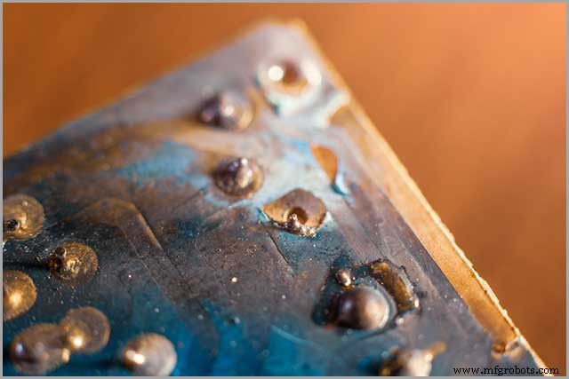
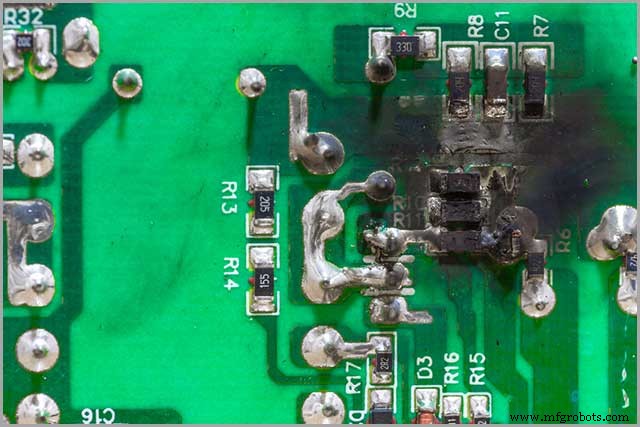
4。 Solder joint defects
As a PCB manufacturer, solder joint abnormalities is something that you’d want to avoid at all times. Weld common errors may occur due to overheated joints, cold joints, welding balling, or excessive solder use. Also, insufficient wetting, solder skips, and solder splashes could bring about weld joint defects.
5。 PCB assembly of small parts
The assembly of small PCB parts is a problem that many designers strive to solve. The main challenge arises, especially when a manufacturer lacks special SMT equipment. Manual placement of such small parts may produce boards that won’t function as intended.
6。 Problems with dispensing method
PCB dispensing is a process of transferring adhesive onto the printed circuit board solder mask. Dispensing ensures that all the components stay in the right place until the PCB gets wave soldered. Choosing the wrong dispensing method is another PCBA problem. Robotic distributing is one of the best-dispensing ways that you can use.
7。 Assembly of regular and irregular patches
A PCB consists of regular and uneven pieces. Some parts have to fit together while others have to stand on their own. Unfortunately, when it comes to the assembly of PCBs, many producers fail in assembling irregular pieces. More often, such needs specialized machines and expertise, and many firms lack such.
8。 Material adhesion problems during PCB assembly
Adhesion is the process of matching different types of materials to one another. High-quality adhesives are necessary during PCB assembly. The reason is that the materials are of high quality and comes with the promise of proper PCB functionality.
9。 PCB assembly process solves the heat dissipation problem
When it comes to PCBA, heat management is essential. A printed circuit board whose design cannot dissipate heat effectively will see a production of equipment that won’t operate properly. Boards that can’t dissipate heat are bound to fail in the end.
10. Design for Manufacturing (DFM)
Also known as DFM, in short, design for manufacturing is an engineering practice that PCB designers use to come up with products that are easy to use. DFM examines the design of a product based on its functionality, tolerances, and materials. Before purchasing PCBs, you need to ensure that the producers had DFM considerations at the back of their minds.
PCB Assembly Service
A printed circuit board populated with electronic parts is a printed circuit board assembly. In its free use, printed circuit board assembly (PCBA) commonly stands for “printed circuit assembly” that consist of components.
• PCB assembly characteristics
PCB assembly involves the entire process of connecting electronic components with the wirings of a PCB. Here, there’s the use of specialized equipment and tools required to achieve this.
• Parts procurement
A PCB is made of several components such as diodes, anodes, solder mask, and wires, to mention but a few. Parts procurement is necessary for PCBA. Parts procurement includes the identification of a need, the negotiation of a contract, vetting, and the selection of the best vendor.
• Service
This involves the selection of the best PCBA services around. There are plenty of PCBA service providers around. However, not all of them are good at their work. Service selection involves picking the best in the field.
• Overview of assembly capabilities
To ensure that your electronic components function correctly, you may have to source or use PCBs manufactured by firms with impressive assembly capabilities. Is the firm of your choice able to do conformal coating and potting? What about knowledge in PTH technology? Ensure that you work with a firm equipped in automated solder paste application, automatic optical inspection, and SMT reflow or wave soldering.
• Assembly equipment
The type of assembly equipment matters a lot. Standard or substandard assembly equipment may see you producing PCBs that aren’t fit for the market. As a manufacturer, you need to ensure that you use state-of-the-art equipment that produces high-quality PCBs.
• Quality Assurance
As a printed circuit board assembler, you need to ensure that you maintain the desired level of quality for your products. You can achieve this by paying particular attention to every stage of the manufacturing process.
总结
Your printed circuit boards will function properly in your electrical components if you get to understand all the above aspects. Your printed contact us. We have a professional PCB production factory here, if you are interested, you can visit it. I hope this article is helpful to you.
工业技术