

石墨烯/TMDs 异质结构的制备和光谱特性研究
摘要
由二维材料组成的范德华 (vdWs) 异质结构受到广泛关注,这是由于其具有吸引力的电学和光电特性。本文首先采用化学气相沉积(CVD)方法制备了高质量的大尺寸石墨烯薄膜;然后,将石墨烯薄膜转移到 SiO2/Si 衬底上;接下来,通过常压化学气相沉积法制备了石墨烯/WS2和石墨烯/MoS2异质结构,这可以通过在石墨烯/SiO2/Si衬底上直接生长WS2和MoS2材料来实现。最后,通过AFM、SEM、EDX、拉曼和PL光谱对石墨烯/TMDs异质结构进行测试表征,以获得和掌握形态和发光规律。测试结果表明,石墨烯/TMDs vdWs异质结构具有非常优异的薄膜质量和光谱特性。石墨烯/TMDs异质结界面处存在内置电场,可以有效分离光生电子-空穴对。单层WS2和MoS2材料具有很强的宽带吸收能力,WS2的光生电子可以转移到下面的p 型石墨烯,当石墨烯/WS2 异质结构材料暴露在光线下时,剩余的空穴可以诱导光门效应,这与普通的半导体光电导体形成鲜明对比。石墨烯/TMDs异质结构光谱特性的研究可为新型光电器件的应用铺平道路。
介绍
随着芯片集成度的提高,传统的硅基金属氧化物半导体(CMOS)晶体管的尺寸越来越小,器件的制备工艺也变得更加复杂,因此研究人员开始关注超薄异质结构基光电子学 [1, 2]。二维 (2D) 异质结构可以通过层之间的弱范德华 (vdWs) 力和层的强共价键结合。这些层可以通过破坏弱范德华键来分离,然后很容易转移到其他基材上 [3]。通过堆叠不同的二维材料可以形成新的原子级二维 vdWs 异质结构,二维异质结构的协同效应变得非常重要。同时,异质结构中相邻晶体之间存在电荷重排和结构变化,可以通过调整各元素材料的相对取向来调节。不同的异质结构不仅可以保持单一材料的性能,而且可以在协同效应下产生新的物理特性[4,5,6]。 vdWs异质结构是探索新的物理现象和规律的物质保证,可以为具有优异光电性能的纳米电子器件提供更多的可能性。
由于二维晶体材料对光有很强的相互作用,它们作为光敏材料引起了广泛的关注[7]。石墨烯是具有优异电学、光学和机械性能的原子级二维材料,在光电子领域有着广泛的应用[8,9,10]。然而,零带隙的缺陷限制了石墨烯的应用和发展。二维过渡金属二硫属化物(TMDs)材料的结构类似于石墨烯,其带隙宽度随层数和厚度而变化[11, 12]。将优势互补的TMDs和石墨烯材料叠加在一起,可以促进石墨烯和TMDs材料在光电检测领域的应用[13,14,15]。石墨烯的高迁移率可以保证器件的快速响应,TMDs材料电子态密度的范霍夫奇点保证了光与材料之间的强相互作用,可以有效增强光的吸收和电子-空穴对的产生[16, 17]。二维异质结构因其电荷隧穿或电荷积累的输运特性、灵活的能带工程和独特的层间激子特性而被广泛应用于新型电子和光电器件中。因此,石墨烯和TMDs材料之间的层间协同相互作用可以有效地控制异质结构的能带结构、磁性能和激子性能。石墨烯/TMDs 异质结构具有高光敏性和光响应性能,这是由于强量子限制效应 [18, 19]。目前,关于大面积、大尺寸、高质量石墨烯/TMDs异质结构可控制备方法的研究较少。而且异质结构的制备过程复杂,在重复性和可控性方面仍然是一个很大的挑战[20, 21]。此外,石墨烯/TMDs异质结构的光谱特性难以理解和掌握,极大地阻碍了石墨烯/TMDs异质结构在未来光电器件中的应用[22]。
在本文中,石墨烯/WS2 和石墨烯/MoS2 异质结构由三种不同介电常数、带隙宽度和吸收系数的半导体材料组成。二维材料直接生长在SiO2/Si衬底的单晶石墨烯薄膜上形成石墨烯/TMDs异质结构,可以保证异质结构的界面清洁和原子能级跃迁。石墨烯、MoS2和WS2的结构可以通过AFM、SEM、EDX、拉曼和光致发光光谱分析,掌握石墨烯/TMDs异质结构的光谱特性,可用于制备高速电子迁移晶体管( HEMT) 和光电探测器 [23,24,25]。
方法
石墨烯的制备和运动
大面积、高质量的石墨烯薄膜是通过CVD系统制备的,该系统由管式炉、气体混合系统和真空机组成。首先,将尺寸为 10 cm × 10 cm 的铜箔放入 1 mol/L 盐酸溶液中进行 3 分钟超声波清洗。然后依次用水和乙醇洗涤。随后,通过吹氩气将其干燥。最后,将其插入石英管的中间,我们安装了系统并校正了气压 [26](图 1)。
<图片>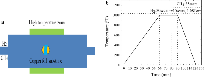
一 石墨烯生长和b的CVD系统图 石墨烯生长过程中的温度曲线
众所周知,多晶铜箔会影响石墨烯的质量,因此在进行石墨烯生长实验前需要对铜箔基板进行退火处理。阶段1退火工艺的具体条件如下:退火温度、时间和氢气(H2)气体的流速分别为1000℃、20分钟和30sccm。此时,铜箔表面会形成大面积的单晶畴,氢气可以还原氧化铜,从而获得高纯度的铜基板。进入第2阶段生长温度保持不变,H2气流量调整为10sccm,同时引入35sccm甲烷(CH4)气体,生长时间和生长压力分别保持10分钟和1.08 Torr,在我们的 CVD 实验中石墨烯的生长速率约为 16 μm/s,这将确保制备相对均匀的单层石墨烯薄膜 [27, 28]。最后将管式炉按一定速率淬火至室温,避免损伤基体表面。
下面描述了单层石墨烯材料到 SiO2/Si 衬底的转移特定过程 [29]。首先,将质量分数为 4% 的 PMMA 溶液均匀旋涂在尺寸为 1 cm × 1 cm 的单层石墨烯材料表面,转速和时间分别为 3000 R/min 和 1 min。接下来,铜箔基板用质量分数为 3% 的 (NH4)2(SO4)2 溶液蚀刻,处理时间为 3-4 小时。然后,将载玻片上的 PMMA/石墨烯在去离子水中反复冲洗 2-3 次,通过 SiO2/Si 衬底将 PMMA/石墨烯去除到 50°C 恒温台,这样可以去除单层石墨烯之间的水蒸气材料和SiO2/Si衬底,单层石墨烯材料可以更好地附着在SiO2/Si衬底上。在这一步中,SiO2/Si 衬底的尺寸为 1 × 1 cm 2 用丙酮、乙醇和水超声清洗 15 分钟,SiO2/Si 衬底表面非常干净和均匀,有利于石墨烯/TMDs 异质结构的生长。最后,将 PMMA/石墨烯/SiO2/Si 放入丙酮溶液中 3-4 h 溶解 PMMA,并用酒精和去离子水反复清洗,以确保单层石墨烯薄膜可以转移到 SiO2/Si 衬底上。
石墨烯/TMDs 异质结构的制备
在CVD双温区管式炉中,石墨烯/SiO2/Si衬底用于生长MoS2和WS2材料。 MoO3、WO3 和硫粉分别用作生长钼源、钨源和硫源。高纯 Ar 气也分别用于制备石墨烯/MoS2 和石墨烯/WS2 异质结构。首先,将装有 100 毫克硫粉的石英舟放在管式炉的上游。然后,将 2 mg MoO3 粉末(或 WO3 粉末)装入另一个石英舟中,将石墨烯/SiO2/Si 衬底倒置在 MoO3 粉末(或 WO3 粉末)上。然后,将装有石墨烯/SiO2/Si 衬底和MoO3 粉末(或WO3 粉末)的石英舟插入管式炉的高温区。将加热带缠绕在石英管上对硫粉进行加热,这样可以确保硫粉得到很好的控制和均匀蒸发,如图 2a 所示。接着以流速为50sccm的高纯Ar气为载气,硫粉蒸发温度控制在150℃,MoS2和WS2的生长温度和生长时间分别为750℃、920℃。分别为 °C 和 10 分钟。同时,将第一段温度保持在100°C 10分钟,可以去除管式炉的水蒸气。具体的温度变化图如图 2b 所示。随后,硫磺粉开始升华成硫蒸气,硫蒸气到达管式炉高温区,可用氩气驱动。可与MoO3和WO3粉末充分反应,产物沉积在石墨烯/SiO2/Si衬底上。因此,石墨烯/TMDs 异质结构的生长速度与 TMDs 材料的生长速度一致 [30]。 MoS2和WS2材料生长后,管式炉自然冷却至室温,基材颜色变为淡黄色。
<图片>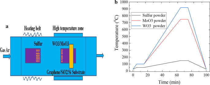
一 石墨烯/TMDs异质结构和b的制备示意图 生长温度与时间的关系曲线
石墨烯/TMDs 异质结构的测试表征
在本文中,石墨烯/TMDs异质结构的测试和表征方法主要包括光学显微镜(OM)、拉曼和光致发光(PL)光谱、场发射扫描电子显微镜(FESEM)、能量色散X射线光谱( EDX) 和原子力显微镜 (AFM)。首先,可以通过光学显微镜、SEM 和 AFM 观察石墨烯/TMDs 异质结构的表面形貌。异质结构的层数可以根据异质结构样品的对比度不同来判断。然后,测试和表征了石墨烯/TMDs异质结构的光谱特性。基于表征结果,分析和推测了 TMDs 材料在石墨烯表面的生长形态、生长模式和生长机制 [31]。其次,拉曼光谱在表征二维材料方面具有快速、高效和低破坏性的优势。它可以直接观察到电子声子在样品表面的相互作用,在二维材料中有着非常广泛的应用。通过分析拉曼光谱特征峰位、特征峰位波数差等石墨烯/TMDs异质结构特征,可以有效判断二维材料的层数和晶体质量。最后,PL 光谱也是表征和分析二维材料的重要方法。当块体材料减薄为单层材料时,TMDs材料的带隙宽度从间接带隙半导体变为直接带隙半导体。同时荧光效果显着增强,PL光谱中有明显的特征峰。然而,如果石墨烯/TMDs异质结构的晶体质量不高,即使样品具有很少的层或单层,PL光谱的特征峰强度也会很小。因此,样品的层厚和晶体质量也可以通过PL光谱来判断。此外,石墨烯/TMDs异质结构薄膜的分布、元素类型和浓度百分比可以通过FESEM和EDX获得。同时,AFM测试也用于掌握异质结构薄膜样品的表面清洁度、粗糙度和材料厚度。
PL和拉曼光谱均由HORIBA Jobin Yvon(法国公司)生产的LabRAM HR Evolution高分辨率拉曼光谱仪收集[32, 33]。拉曼和 PL 光谱的范围为 300 cm -1 –3000 cm -1 和 550–800 nm,分别。拉曼光谱和 PL 光谱分别为 10% 功率和 5% 功率。以下为具体测试条件,光谱分辨率 ≤ 0.65 cm −1 ;空间分辨率:水平 ≤ 1μm,垂直 ≤ 2μm; 532 nm 激光器,50 倍物镜(光束光斑直径为 1.25 μm,100% 激光功率相当于 7500 μw/cm 2 );扫描时间15s,累计次数为2次。
结果与讨论
石墨烯/WS2 异质结构的光学显微照片和表征
拉曼光谱仪的高分辨率显微镜可以区分异质结构的形态。图 3a 显示了 SiO2/Si 衬底不同位置下石墨烯/WS2 异质结构的光学显微镜图像。由于转移到SiO2/Si衬底上的石墨烯薄膜颜色差别不大,因此石墨烯薄膜比较均匀完整。除了少量颗粒外,石墨烯/SiO2/Si 衬底的表面是干净的,这表明存在质量更好的石墨烯薄膜。同时,在WS2的生长实验中,当气体浓度足够时,WS2的成核密度最大。并且在石墨烯/SiO2/Si 衬底上生长的 WS2 是三角形结构的晶粒,晶粒表面均匀,边长约为 120 μm。 WS2的形状规则完整,厚度均匀,远大于机械剥离样品的尺寸[34]。在图 3b 中,由于 WS2 样品的荧光强度分布高度均匀,三角形单层 WS2 膜具有更高的质量和更低的缺陷。从图 3c、d 可以看出,WS2 薄膜样品的形貌为三角形,WS2 薄膜的厚度为 0.83 nm,表明制备的是单层 WS2 薄膜。此外,还使用SEM分析了WS2样品膜的形貌,形貌为厚度均匀的规则三角形,如图3e所示。在图3f中,EDX光谱中显示了dock元素、硫元素和碳元素,表明石墨烯/WS2异质结构材料成功转移制备。
<图片>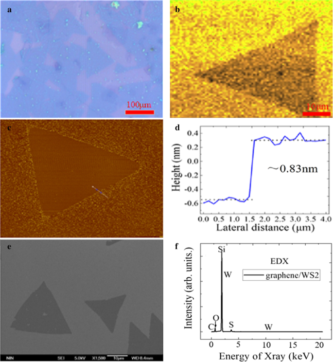
一 光学显微照片,b 映射图像,c AFM 图像,d 身高轮廓图像,e FE-SEM 图像和 f SiO2/Si衬底上石墨烯/WS2异质结构的EDX光谱
材料的分子振动和旋转信息可以通过拉曼光谱获得,是用于识别材料结构的指纹振动光谱。 WS2样品的层数和晶体质量可以通过拉曼光谱的特征峰位置和波数差来有效判断。图 4a 显示了 WS2 样品在不同位置的拉曼光谱,E 1 2g 和 A1g 特征峰位于 350.4 cm -1 和 416.1 厘米 −1 , 分别。当块体 WS2 变为单层材料时,E 1 2g和A1g特征峰分别出现蓝移和红移。因此,可以通过两个特征峰的波数差来判断层数,波数差为65.7 cm -1 ,所以三角形 WS2 晶粒是单层材料。在图 4b 中,最强的发光峰位于 626 nm,相应的带隙为 1.98 eV,与单层 WS2 的带隙宽度一致。众所周知,二维材料的PL强度与晶体质量和层数有关。二维材料的缺陷和层数较少,发光强度较高,表明晶体质量较好[35]。可变功率表征可以在 nW 级别执行,以防止激光照射损坏样品。通过观察图 4c 可以发现 E 1 的峰值位置 随着激发功率的增加,2g平面振型基本保持不变,平面间A1g振型向短波数方向移动。这是因为A1g振动模式与电子浓度有很大的关系,电子浓度的增加会导致带隙的重新形成。如图 4d 所示,WS2 的 PL 光谱强度随着激光功率的增加而增加,并且存在荧光猝灭现象,这是由于带隙的重新形成和异质结构的层间相互作用。同时还可以发现,材料的局部温度几乎没有随着激光功率的增加而变化。这是因为WS2是原子层级纳米材料。
<图片>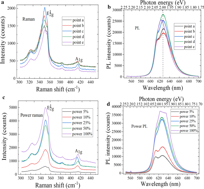
WS2 的光谱表征。 一 不同位置的拉曼光谱,b 不同位置的PL光谱,c 功率拉曼光谱和d 功率PL光谱
石墨烯材料的层数表征和质量信息可以通过拉曼光谱获得。在图 5a 中,石墨烯在不同位置的拉曼衍射光谱具有三个主要特征峰,D 峰、G 峰和 2D 峰,分别位于 1330 cm -1 , 1583 厘米 −1 和 2674 厘米 −1 . D峰与石墨烯晶格结构的无序有关,当石墨烯材料的晶格缺陷较多时,D峰的位置发生蓝移,可以反映晶体的缺陷和杂质含量。二维峰为双声子二阶共振拉曼峰,可以表示石墨烯材料的碳原子排列。此外,G峰是由第一布里渊区中心的E2g模式引起的,峰高随石墨烯层数的增加几乎呈线性增加,G峰强度在一定程度上与石墨烯的掺杂有关。 2D峰与G峰的相对比值可以粗略地确定石墨烯的层数,随着缺陷密度的增加,D峰与G峰的比值会降低。当MoS2(或WS2)材料生长完成时,石墨烯的拉曼光谱中出现弱D峰,表明石墨烯畴仍保持高质量。暴露的石墨烯区域的二维峰强度减弱,这是受高温生长过程的影响。石墨烯二维峰的半峰全宽(FWHM)随着层数的增加而逐渐增大,二维峰的峰位置发生蓝移,这可能与石墨烯材料的能带关系有关。电子能带结构随着层数的增加而分裂,并且会发生各种声子共振散射过程。激子峰会通过吸收更多的能量而被激发,这将导致二维峰位置的蓝移。 C点和E点的G峰的峰强度明显高于2D峰的峰强度。 我 二维/我 G比随着厚度的增加而降低,本实验中转移的石墨烯不是很均匀,在允许范围内。图 5b 显示了单层石墨烯的功率拉曼光谱。石墨烯的 G 和 2D 峰强度随着激光功率和温度的增加而逐渐增加,峰位和 FWHM 基本没有变化。 G 峰和 2D 峰分别位于 1581 cm -1 和 2672 厘米 −1 ,并且两个特征峰的强度相差很大。由于石墨烯与底层 SiO2 之间的相互作用变化,I 的特征峰比 二维/我 G 减少。同时,拉曼光谱没有出现D缺陷峰,表明所选择的石墨烯区域质量高,碳原子高度有序。
<图片>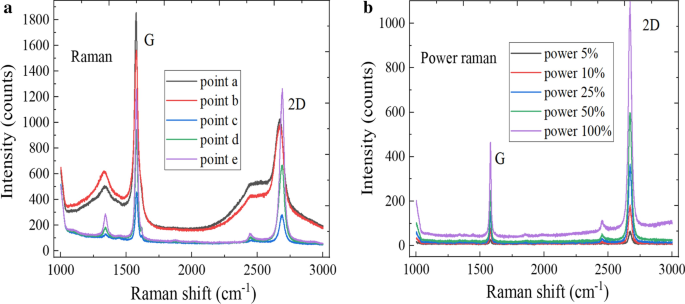
石墨烯的光谱表征。 一 不同位置的拉曼光谱和b 功率拉曼光谱
拉曼光谱用于表征和分析石墨烯/WS2异质结构材料,有两个300 cm -1 光谱 ≤ ω ≤ 500 cm −1 和 1400 厘米 −1 ≤ ω ≤ 3000 cm −1 ,由洛伦兹函数拟合。有 E 1 WS2 在 300 cm −1 范围内的 2g 和 A1g 模式特征峰 ≤ ω ≤ 500 cm −1 . E 1 2g声子模是硫原子和钨原子的面内位移,而A1g声子模是硫原子的面外位移,上述声子模的位置和间隔随层数而变化。石墨烯的 G 和 2D 峰出现在 1400 cm -1 的光谱区域 ≤ ω ≤ 3000 cm −1 ,根据强度比和特征峰的峰位可以得到石墨烯的层数和晶体质量信息。
两个不同的 Davydov 分裂峰的频率差异可以反映 vdWs 异质结构的相互作用幅度。因此,多层二维材料的层内振动声子模式频率也取决于层间耦合和层数。图 6a 显示了石墨烯/WS2 异质结构在 532 nm 激光下不同点的拉曼光谱测试表征。可以发现,E 1 的强度 2g特征峰强度高于A1g特征峰强度,E 1 2g 和 A1g 特征峰位于 349.3 cm -1 和 417.1 厘米 −1 , 分别。石墨烯/WS2 异质结构的拉曼光谱 2D 和 G 峰分别位于 1591.5 cm -1 和 2680.9 厘米 −1 ,且2D和G峰的峰位与纯石墨烯相比升高,这可能与WS2纳米片的有效层间耦合和CVD生长过程中高温加热产生的应变效应有关。石墨烯/WS2异质结构材料的拉曼光谱只是单独分离的WS2和石墨烯光谱的总和,可以证实vdWs异质结界面的形成。 PL 光谱强度与晶体质量和层数有关。拉曼光谱侧重于异质结构形成对振动模式的影响,TMDs异质结构材料的电子能带结构主要可以通过PL光谱获得。图 6b 显示了石墨烯/WS2 异质结构在不同点的 PL 光谱。最强的发光峰位于 624 nm,相应的带隙为 1.99 eV,与单层 WS2 的带隙宽度一致。不同位置的石墨烯/WS2异质结构材料具有不同的PL光谱强度和形状,晶体质量不是很好。因此,异质结构的制备工艺有待进一步改进。石墨烯/WS2异质结构的PL光谱强度比WS2弱。这是因为石墨烯/WS2异质结构的层间耦合改变了异质结构区域的激子荧光,这将导致电子-空穴对的分离和荧光的降低。同时,石墨烯/WS2异质结构形成时峰位发生偏移,电荷的转移会引起费米面的偏移,使自由激子转变为带电激子。图 6c 显示了石墨烯/WS2 异质结构的功率拉曼光谱。面内声子模 E 1 2g 特征峰和面外声子模式 A1g 特征峰分别位于 356 cm -1 和 418 cm −1 ,其中上述特征峰值随着激光功率的增加而增加。单晶内特征峰的峰位和形状均一,石墨烯/SiO2/Si衬底上WS2的电子特性均一。根据A1g和E 1 的频率差可以确定WS2片材的厚度 2g特征峰,平均距离为62 ± 0.2 cm −1 ,这与单层 WS2 的厚度一致。与本征石墨烯的峰位置相比,石墨烯/WS2 异质结构的 G 峰和 2D 峰位置来自 1578.7 cm -1 和 2685.8 厘米 −1 更改为 1582.2 cm −1 和 2689.5 厘米 −1 , 分别。此外,随着激光功率的增加,G峰的强度强于二维峰的强度,I 二维/我 G 比,这是由石墨烯和 SiO2/Si 衬底之间的相互作用变化引起的 [36, 37]。观察图6d可以发现石墨烯/WS2异质结构的PL强度随着激光功率的增加而增加, PL 光谱的 FWHM 也增加,PL 光谱的形状发生变化。原因是异质结构周围的测试温度升高,石墨烯/WS2异质结界面处也存在强层间耦合。
<图片>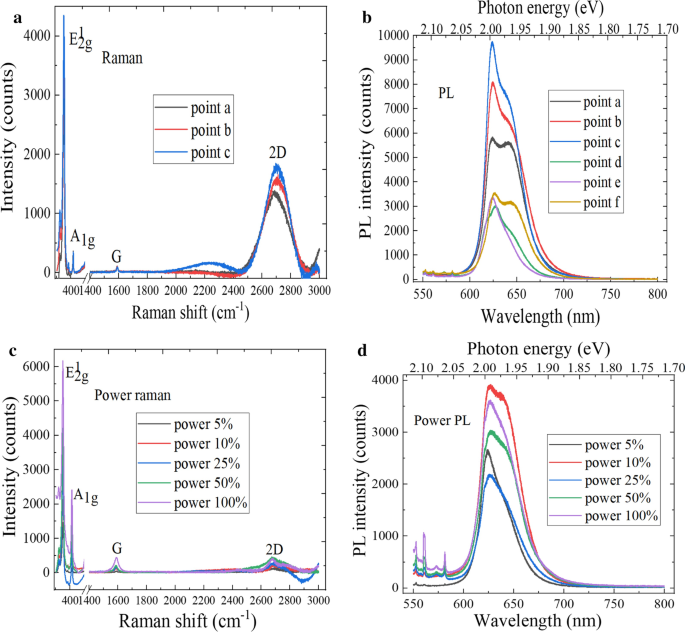
石墨烯/WS2 异质结构的光谱表征。 一 不同位置的拉曼光谱; b 不同位置的PL光谱; c 功率拉曼光谱;和 d 功率PL光谱
石墨烯/WS2 异质结构的拉曼光谱与暴露的石墨烯区域的拉曼光谱显着不同,如图 7a 所示。首先,当波数增加时光谱背景上升,背景来自WS2的PL光谱,这证实了石墨烯/WS2异质结构的存在。其次,WS2材料可以抑制石墨烯的二维特征峰强度。最后,与裸石墨烯材料的光谱相比,石墨烯/WS2 异质结构的 G 峰和 2D 峰都向上移动。由于石墨烯和WS2之间的层间耦合,二维峰也会上移,机械应变也会对石墨烯的拉曼位移产生影响。增强因子(EF)是石墨烯/WS2异质结构的最大峰值强度除以石墨烯的最大峰值强度的比值。 G峰的最大峰强度从460增加到830,2D峰的最大峰强度从340增加到1460,对应的EF分别为1.8和4.3。当形成石墨烯/TMDs 异质结构时,D 峰信号显着增强。因此,I D/我 单层石墨烯的 G 比弱于石墨烯/WS2 异质结构的 G 比。这是因为WS2在石墨烯上的挤出对石墨烯的结构有影响,会导致少量缺陷的出现。 In Fig. 7b, the PL intensity of graphene/WS2 hetero-structure is higher than that of bare graphene, which may be related to the effective interlayer coupling and the strain effect. Meanwhile, the maximum intensity of PL spectra is increased from 270 to 1410, and the corresponding EF is 5.23. The intensity enhancement of characteristic peak can be attributed to the coupling of graphene/WS2 hetero-structure.

一 Raman spectra and b PL spectra characteristics comparison of graphene before and after WS2 growth
Raman spectroscopy can be used to evaluate the crystal quality and film thickness of 2D materials. The Raman spectra comparison of WS2 and graphene/WS2 hetero-structure is shown in Fig. 8a. Compared to the Raman spectra of WS2, the A1g mode characteristic peak position of graphene/WS2 hetero-structure was blue-shifted, and the intensity of E 1 2g mode and A1g mode characteristic peaks was higher than those of WS2, and the graphene/WS2 hetero-structure film has the excellent crystallinity. The reason is that the coupling between layers can be enhanced when the two materials are stacked to form the hetero-structure, which would generate the interlayer interaction forces. The maximum E 1 2g and Alg characteristic peak intensity increases from 3400 and 1100 to 6500 and 2950, respectively. And the enhancement factors (EF) are 1.9 and 2.7, respectively. In addition, monolayer WS2 and multilayer WS2 are the direct band gap semiconductor and indirect semiconductor materials, respectively. Therefore, the PL spectroscopy can be used to identify the layer number of WS2 sample. In Fig. 8b, the above two materials show that the strongest PL emission was around 626 nm, and that the band gap was approximately at 1.98 eV, which is consistent with band gap of the mechanically peeled monolayer WS2. The PL intensity of graphene/WS2 hetero-structure was stronger than that of monolayer WS2. The reasons are the following:First, the work function between graphene and WS2 does not match. Second, the internal field was formed. Third, the photoelectrons from WS2 can transfer to graphene. Forth, the WS2 material retains holes. The maximum intensity of strongest peak increases from 7450 to 19,320, and the EF of PL spectra are 2.6. The increase in peak intensity is due to the coupling between graphene and WS2 materials.

一 Raman spectra and b PL spectra characteristics comparison between WS2 and graphene/WS2 hetero-structure
Optical Micrograph and Characterization of Graphene/MoS2 Hetero-structure
The optical microscope pictures of graphene/MoS2 hetero-structure on SiO2/Si substrate are shown in Fig. 9a. We found that the color of the graphene transferred to SiO2/Si substrate was not much different from the original one. The surface was relatively clean except for a few particles in some areas. These results indicate that the graphene film is uniformly and completely formed. The MoS2 thin film covers graphene/SiO2/Si substrate, which can be connected into the continuous graphene thin film across the grain boundaries. The prepared graphene/MoS2 hetero-structure was continuous and intact, and the sample surface was relatively clean, which has the good surface uniformity. The local fluorescence intensity distribution is not uniform when there are many defects. Figure 9b shows the in-plane fluorescence intensity distribution of triangular monolayer MoS2 film. The crystal lattice of sample has the fewer defects. In Fig. 9c, d, the surface condition of the material is observed by AFM, and the height difference between the edge of the material and the graphene/SiO2/Si substrate is measured to judge the material thickness, the thickness of monolayer MoS2 material is about 0.81 nm. It can be found by the SEM test result that the morphology of MoS2 film sample is the triangular flake, as shown in Fig. 9e. It can be found by observing Fig. 9f that the molybdenum, sulfur and carbon elements are uniformly distributed in the EDX spectrum, which indicates that the graphene/MoS2 hetero-structure has been successfully prepared.

一 Optical micrograph, b mapping image, c AFM image, d height profile image, e FE-SEM image and f EDX spectrum of graphene/MoS2 hetero-structure on SiO2/Si substrate
The interlayer interaction weakens with decrease in the film thickness. The A1g mode characteristic peak is red-shifted, whereas the characteristic peak of E 1 2g mode is blue-shifted. As a result, the frequency distance between A1g and E 1 2g vibration modes becomes smaller, which can be used to identify the thickness of 2D materials. Figure 10a shows the Raman spectra of MoS2 at different positions. The characteristic peaks of E 1 2g mode and A1g mode were at 381.2 cm −1 and 400.5 cm −1 , 分别。 And the peak spacing was 19.3 cm −1 , which indicates the presence of monolayer MoS2. Due to the Van der Waals force between the layers, the frequencies of two vibration modes moving in the same or opposite directions between adjacent atoms in the layers are slightly different. The PL spectra are used to obtain the light emission characteristics of MoS2 film, as shown in Fig. 10b. As we all know, the luminous intensity of monolayer MoS2 was much greater than that of multilayer, and the electronic band structure changed from indirect band gap to direct band gap when the layer number of MoS2 material changed from multilayer to single layer. Therefore, there was only the strong emission peak of monolayer MoS2. In addition, the strongest PL peak was at 678.5 nm, and the corresponding direct band gap was 1.83 eV, which is close to the band gap value of mechanically peeling MoS2 film. It can be found by observing Fig. 10c that the characteristic peak intensity of Raman spectra is increased with increase in the laser power and that the peak positions of E 1 2g and A1g mode characteristic peak were blue-shifted. This is because the Raman peak line would have a certain frequency shift with increase in the temperature and laser power. Figure 10d shows the power PL spectra of MoS2, the luminous intensity increasing accordingly with increase in the laser power, and the strongest PL peak position was blue-shifted.

Spectral characteristics characterization of MoS2. 一 Raman spectra at different positions, b PL spectra at different positions, c power Raman spectra and d power PL spectra
A high-frequency layer vibrating phonon mode of monolayer 2D material would split into the N corresponding high-frequency modes in an N-layer 2D material, which would lead to the Davydov splitting. Figure 11a shows the Raman spectra of graphene/MoS2 hetero-structure, and there were the G, 2D peaks of graphene and the E 1 2g and A1g peaks of MoS2, which indicates the formation of layered graphene/MoS2 hetero-structure material. The E 1 2g and A1g Raman characteristic peaks of MoS2 were located at 375.5 cm −1 and 394.4 cm −1 , 分别。 And the peak spacing was 18.9 cm −1 . Compared with intrinsic graphene, the G peak and 2D peak positions of graphene/MoS2 hetero-structure shift to large wavenumbers, and G peak and 2D peak move from 1581 and 2672 cm −1 to 1587 and 2674 cm −1 , 分别。 In addition, the intensity of G peak is stronger than that of 2D peak. The rise of the 2D and G peaks position is related to the effective interlayer coupling and the strain effect. Compared with the Raman spectra of MoS2 material, the spectra of graphene/MoS2 hetero-structure material are significantly shifted due to the enhancement of interlayer atomic interaction, and the peak intensity can also be significantly enhanced. It can be found from Fig. 11b that the graphene/MoS2 hetero-structure has two absorption peaks at 621 nm and 683 nm and that the corresponding band gaps were 1.99 eV and 1.82 eV according to the conversion relationship between wavelength and electron volt. The luminous intensity of graphene/MoS2 hetero-structure was lower than that of intrinsic MoS2. The reasons of these phenomena are that the graphene material has the weakening effect on the fluorescence of MoS2 material and that the electronic energy band and electronic distribution can be changed due to the interlayer coupling, which can greatly change the PL and Raman spectra.

Spectral characteristics of graphene/MoS2 hetero-structure. 一 Raman spectra at different positions, b PL spectra at different positions, c power Raman spectra and d power PL spectra
Figure 11c shows the power Raman spectra of graphene/MoS2 hetero-structure, the Raman peaks intensity of G, 2D, E 1 2g, and A1g increasing with increase in the laser power. The peak position difference between E 1 2g and A1g is gradually enhanced with increase in the layer number of MoS2 material. The characteristic peak positions of E 1 2g and A1g were 377.2 cm −1 and 396.7 cm −1 , 分别。 And the peak position difference was 19.5 cm −1 , which can be judged that MoS2 material is the monolayer. Meanwhile, the G and 2D peaks of graphene were red-shifted and blue-shifted, respectively. This is because graphene material is doped with MoS2. It can be found by observing Fig. 11d that there were two PL peaks of graphene/MoS2 hetero-structure. These PL peak corresponding to the compound transition of A and B excitons, wherein the light emission corresponding to the direct band gap exciton recombination was 1.84 eV, whereas the peak corresponding to the indirect band gap exciton recombination was at 2.0 eV. The luminous intensity of strongest peak is increased with increase in the laser power, and the peak position of the strongest PL spectra is red-shifted. This is due to the p -type conductivity of the graphene and the change of band structure when graphene and MoS2 materials were stacked. In addition, the arrangement of energy bands at the interface allows the electrons from electron-rich MoS2 to transfer to p -type graphene material.
结论
Graphene/TMDs-based hetero-structures, where WS2 and MoS2 were used as TMDs material, were successfully synthesized directly on graphene films by using APCVD. The morphology, spectral characteristics and luminescence law of hetero-structures can be obtained by AFM, SEM, EDX, Raman and PL spectroscopy, and the hetero-structures show the excellent photosensitivity. Compared with intrinsic graphene material, the G and 2D peak positions of graphene/TMDs hetero-structures are the blue-shifted, the intensity of G peak is stronger than that of 2D peak with increase in the laser power and decrease in the I 二维/我 G ratio. Due to the presence of internal electric field, the photo-generated electron–hole pairs can be effectively separated at the interface of graphene/TMDs hetero-structures, which could greatly improve the light response. This research could effectively guide the preparation process improvement in large-area, high-quality hetero-structures, and it could also pave the way for the application of graphene/TMDs hetero-structures in the optoelectronic devices field.
数据和材料的可用性
The experiment data supporting the conclusion of this manuscript have been given in this manuscript.
缩写
- 2D TMDs:
-
Two-dimensional transition-metal dichalcogenides
- vdWs:
-
范德华
- HEMT:
-
High-speed electron mobility transistors
- PMMA:
-
聚甲基丙烯酸甲酯
- MoS2:
-
二硫化钼
- APCVD:
-
Atmospheric pressure chemical vapor deposition
- WO3:
-
Molybdenum trioxide
- OM:
-
Optical microscopy
- PL:
-
光致发光
- MoO3:
-
Molybdenum trioxide
纳米材料