

碳纳米管组装和应用集成
摘要
碳纳米管 (CNT) 因其独特的性能组合而引起了极大的兴趣,包括高机械强度、大纵横比、高表面积、独特的光学特性、高导热性和导电性,使其适用于广泛的应用领域。从电子(晶体管、能源生产和存储)到生物技术(成像、传感器、执行器和药物输送)和其他应用(显示器、光子学、复合材料和多功能涂层/薄膜)的领域。碳纳米管的可控生长、组装和集成对于当前和未来纳米管应用的实际实现至关重要。本综述侧重于迄今为止在各种应用的 CNT 组装和集成领域取得的进展。首先介绍了基于电弧放电、激光烧蚀和化学气相沉积 (CVD) 的 CNT 合成,包括尖端生长和基底生长模型的详细信息。然后详细探讨了使用催化剂调节、克隆、种子和基于模板的生长等方法在 CNT 结构控制(手性、直径和连接)方面的进展,然后是使用选择性表面化学、凝胶色谱法的生长后 CNT 纯化技术和密度梯度离心。考虑了基于催化剂图案化、森林生长和复合材料的多种 CNT 的各种组装和集成技术,以及使用光刻、转移印刷和不同的基于溶液的技术(例如喷墨印刷、介电泳 (DEP) 和旋转)将它们对准/放置到不同基板上涂层。最后,考虑了碳纳米管在能量存储、晶体管、组织工程、药物输送、电子密钥和传感器等领域当前和新兴应用中的一些挑战。
介绍
碳纳米管 (CNT) 是由石墨片(又名石墨烯)制成的长而中空的圆柱形小管结构,直径范围从 1 nm 以下到 10 s of nm [1]。基于这些石墨烯层卷成圆柱体的方式,CNT 表现出不同的电子特性。纳米管可以是单壁结构,称为单壁碳纳米管 (SWCNT),也可以有许多壁,称为多壁碳纳米管 (MWCNT)。 SWCNTs 可以进一步在电学上分为半导体和金属 SWCNTs(s-SWCNTs 和 m-SWCNTs),而 MWCNTs 主要表现出金属行为。碳纳米管的新颖和有用的特性,例如低成本、轻质、高纵横比和表面积、独特的光学特性、高导热性和导电性以及高机械强度,使它们适用于广泛的电子领域并引起人们的兴趣。 、生物医学和其他工业应用。例如,碳纳米管有望用于“超越 CMOS”的电子产品,作为未来集成电路中的有源器件和互连 [2]。
碳纳米管是富勒烯家族的一部分,富勒烯家族是一组碳同素异形体,其原子以笼状结构的形状连接,例如空心球、椭圆体或圆柱管 [3]。富勒烯由连接六边形和五边形环的石墨烯片组成,这使它们具有弯曲的结构。石墨烯是碳的同素异形体,由单层碳原子组成,排列在二维六边形晶格中。它是一种半金属,价带和导带之间有重叠,即它具有零带隙 [1]。巴克敏斯特富勒烯 (buckyball/C60) 是最常见的球形富勒烯之一,是一种具有 60 个碳原子的纳米级分子,每个原子与其他三个相邻原子键合形成六边形和五边形,末端弯曲成球体。 C70 分子是另一种球状富勒烯,化学性质稳定。此外,还发现了其他较小的亚稳态物种,例如 C28、C36 和 C50。人们相信富勒烯在自然界中已经存在很长时间了;已经发现隐藏在烟灰中的微量富勒烯以 C60、C70、C76、C82 和 C84 的形式存在 [3, 4]。纳米管由 sp 2 组成 -杂化碳键,比sp 3 更强 -在金刚石中发现的杂化碳键,从而使纳米管具有非凡的强度和刚度。此外,已知它们具有非常高的电导率 [5, 6]、高电荷载流子迁移率 [7]、高化学稳定性 [8, 9]、大比表面积 [10]、高纵横比 [11]、优异的机械性能 [12, 13] 和出色的导热性 [14],一些 SWCNT 表现出超导性 [15, 16]。这些特性使碳纳米管成为纳米科学和电子学研究的重要课题[17]。
单个 SWCNT 的比表面积 (SSA) 理论上已获得为 1315 m 2 g −1 ;但由于管子的捆扎、结块和纯度,测得的表面积要低得多 [10]。例如,SSA 值在 150 到 790 m 2 之间的 SWCNT 试样 g −1 已获得[10]。对于 MWCNT,壁的数量是决定 SSA 的主要参数。一些测量的 SSA 值包括 680–850 m 2 g −1 对于两壁碳纳米管和 500 m 2 g −1 对于三壁碳纳米管 [10]。此外,碳纳米管具有显着的机械性能。单个 MWCNT 的弹性模量约为 1 TPa,而 MWCNT 的拉伸强度范围为 11 至 63 GPa [12, 13]。另一方面,对于单个 SWCNT,已获得约 22 GPa 的拉伸强度值 [12]。直接测量单个 SWCNT 的杨氏模量,估计在 0.79 到 3.6 TPa 之间 [12, 13, 18] 而对于单个 MWCNT,获得的值在 0.27 到 2.4 TPa 之间 [12, 19]。薄 MWCNT 的抗压强度估计在 100 到 150 GPa 之间 [20]。碳纳米管还具有良好的热性能。单个 SWCNT 的热导率值介于 3500 和 6600 W m -1 K −1 在室温下,超过了金刚石的热导率 [14, 21],而单个 MWCNTs 的热导率范围为 600 至 6000 W m -1 K −1 [21]。碳纳米管还具有有趣的尺寸特性。它们的纵横比(长度与直径)值可能非常高。典型的碳纳米管直径值在 0.4 到 40 nm 之间变化(即大约 100 倍),但长度可以变化 10,000 倍,达到 55.5 cm,因此纵横比可以非常高 [11]。
碳纳米管还具有独特的电子特性。碳纳米管独特的电子特性与其独特的低维能带结构和量子限制载流子有着内在的联系。 SWCNT 可以是金属的或半导体的,这取决于石墨烯晶格相对于管轴的直径和取向,称为管的手性 [1, 22]。基向量a 1 和 a 2 确定石墨烯晶格。手性载体 (C ),对应于最终成为 CNT 周长的石墨烯片的一侧由下式给出:C =na 1 + ma 2、其中n 和 m 是整数。石墨烯片可以以不同的方式卷起以生成三种不同类别的 SWCNT,如图 1a-c 所示。此外,每个 CNT 的电子特性源于管的几何形状,由其手性矢量决定。如果 m =0 , C 位于 a 1 或 a 2 并且纳米管将被称为锯齿形碳纳米管,而如果 n =m , C 正好位于 a 之间的方向 1 和 a 2 管被称为扶手椅纳米管。最后,当n ≠ m时形成手性纳米管 .图 1b 显示了如何根据手性指数和相应的手性角定义不同类型的 CNT。所谓的区域折叠方案 [23] 内的分析表明,扶手椅管总是金属的,而三分之二的锯齿形管是半导体的。更一般地说,预计所有 SWNT 中有三分之二是半导体,其余为金属或具有小带隙(准金属)。
<图片>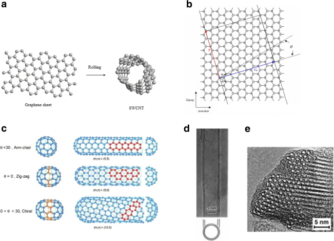
一 通过滚动单层石墨形成 SWCNT。 b 从理想的石墨片形成 CNT 的图示。手性向量的两端C h 叠加以创建具有一维晶格矢量 T 的纳米管 和手征角ϴ . 一 1 和 a 2 是二维石墨的原始晶格向量(白点表示晶格品脱)。还标明了之字形和扶手椅包装方向。 c 基于其手性的不同类型的碳纳米管。改编自 [22]。 d 直径为 5.5 nm 的双壁 CNT 的电子显微图像。改编自 [78]。 e 一束 ~ 100 个 SWCNT 的电子显微镜图像,这些单壁碳纳米管堆积在三角形晶格中。改编自 [17]
CNT 具有极高的电荷载流子迁移率,因此,它们有可能被考虑用于各种电子设备应用 [24]。已经取得了很大进展,表明 SWCNT 是先进的准一维 (1D) 材料,具有高载流子迁移率。碳纳米管中载流子迁移率的估计值范围为 20 cm 2 V −1 s −1 [7] 到非常大的值 (~ 10 4 或更高)在半导体管中和在金属管中弹道 [25]。电流密度介于 10 7 一个厘米 −2 和 10 8 一个厘米 −2 SWCNT 是可以实现的,SWCNT 能够通过大约 20 μA 的电流 [26]。弹道 SWCNT 的电阻在 6.5 到 15 kΩ 之间。多壁碳纳米管通常是金属的 [1],并且具有非常高的载流能力,范围从 10 6 到 10 9 一个厘米 −2 [26, 27]。已证明半导体碳纳米管的带隙与其直径成反比(图 2a),由 E 给出 间隙 =2γ 0 一 C-C /d , 其中 y o 表示 C-C 紧密结合重叠能(2.45 eV),a C-C 是最近邻 C-C 距离 (0.142 nm) 和 d 是管子的直径 [28, 29]。例如,半径为 0.2 nm 的半导体碳纳米管的带隙约为 2.2 eV,而半径为 1.4 nm 的管的带隙约为 0.4 eV [30]。
<图片>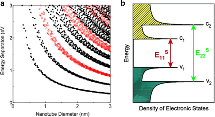
一 Kataura 图将碳纳米管中的带隙能量与其直径相关联。这里,红色圆圈表示半导体碳纳米管,黑色圆圈表示金属碳纳米管。改编自 [32]。 b 示意图显示了半导体 CNT 的态密度和 VHS 峰(由尖锐的最大值表示)。箭头表示光吸收和发射的机制。改编自 [36]
由于波函数边界条件随 (n , m ) 管的指数或手性。因此,通过用光子探测 CNT 样品,吸收、光致发光和拉曼光谱等光学特性可用于广泛地对 CNT 进行快速和非破坏性研究 [31,32,33]。当暴露在光线下时,CNT 还表现出独特的光点燃特性 [34, 35],从而导致声波的产生和 CNT 的氧化。光谱的结果可以用 Kataura 图来记录,其中每个点代表光学跃迁能量 E ii (i =1, 2, 3, ...) 对于特定的 (n, m ) SWCNT 绘制为管直径的函数,如图 2a 所示。一维晶体的状态密度 (DOS) 不是能量的连续函数,而是具有尖峰状 DOS,它以不连续的尖峰上升和下降。这些尖锐的尖峰或范霍夫奇点 (VHS) 使 CNT 具有独特的光学特性 [32]。由于尖峰的存在,CNT 中的光吸收不同于大多数体材料中的吸收。当单壁碳纳米管吸收光时,价带 VHS 中的电子被提升到导带中相应的能级。在纳米管中,光吸收与 v 的急剧电子跃迁有关 2 到 c 2 (能量 E 22 ) 或 v 1 到 c 1 (E 11)水平(图2b)[36]。这些跃迁被探测,然后用于识别纳米管类型[32]。
除了碳纳米管的光吸收特性外,通常研究的另一个光学特性是其光致发光。光致发光用于测量碳纳米管样品中半导体纳米管种类的数量。半导体 SWCNT 在被光子激发时会发出近红外光,这种特性称为光致发光 [37]。当半导体单壁碳纳米管中的电子吸收激发光时,会产生 E 22 跃迁(半导体单壁碳纳米管中从价带到导带的电子跃迁),产生了电子-空穴对。电子和空穴都迅速弛豫,从 c 2 到 c 1 来自 v 2 到 v 1 个状态,分别。最后,它们通过 c 重新组合 1 - v 1 跃迁导致光发射 [32]。在金属管中不能产生激子发光——虽然它们可以产生电子-空穴对,但这些空穴会立即被金属中可用的许多电子中的其他电子填充,因此不会产生激子。
拉曼光谱是另一种用于 CNT 表征的光学技术,它能够检测半导体和金属管 [38],并且通过拉曼显微镜也可以提供良好的空间分辨率。在拉曼光谱中,光子用于激发 CNT 样品并被样品中的声子散射。对激发光子和释放光子之间频率变化的分析主要是通过直径相关的径向呼吸模式来判断样品中的碳纳米管类型 [23]。单壁碳纳米管中的拉曼散射也可以是共振的,这意味着只有具有等于激发激光能量的带隙之一的管才会被选择性探测,并具有增强的吸收截面。
上述CNT特性的选定数值数据列于表1中:
由于其独特和理想的特性,迄今为止,碳纳米管已经发现了许多应用并被纳入了几种商业产品中。
半导体 CNT 已用于场效应晶体管 (FET) [7, 45,46,47,48](图 3 显示了原理图和 I -V CNT 场效应晶体管 (CNTFET) 的特性对不同的栅极电压表现出切换);金属碳纳米管用作互连 [49, 50];单壁和多壁纳米管也已用于各种太赫兹应用(如下所述)和肖特基二极管 [51]。碳纳米管目前正用于锂离子电池中以实现高效的能量存储 [52, 53];氢燃料电池 [54] 和 CNT 涂层已广泛用于检测氨、氢和甲烷等气体 [55]。超取向碳纳米管薄膜已用于液晶显示器(LCD)[56];碳纳米管在透明导电薄膜中也有应用[57]。
<图片>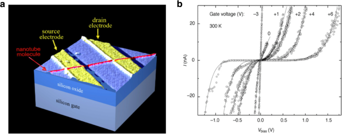
一 初始 CNTFET 演示的示意图。晶体管可以通过向硅衬底(背栅)施加栅极电压来导通,该电压将载流子引入桥接源极和漏极的纳米管通道。改编自 [45]。 b 我 -V CNTFET 的特性显示了在不同栅极电压下欧姆和非线性行为之间的切换。改编自 [48]
已发现 CNT 材料复合材料具有增强的特性。例如,与纯环氧树脂基体相比,碳纳米管增强环氧树脂复合材料的拉伸强度增加了 24.8% [58]。此外,通过将少量磁性排列的碳纳米管引入碳纤维增强聚合物复合材料,弯曲模量和承载能力分别增加了 46% 和 33% [59]。此外,填充有碳纳米管和膨胀型阻燃剂的热塑性聚氨酯 (TPU) 基复合材料显示出具有良好的阻燃性、快速自熄性、良好的电磁干扰屏蔽性能和增加的导电性 [60]。此外,将 CNT 粉末与聚合物混合将增加承载应用的刚度、强度和韧性 [61, 62]。 MWCNTs——磁荧光碳量子点,一种碳纳米管复合材料,已被用作癌症治疗中靶向药物转运的载体[63];含有分散的碳纳米管的纳米流体显示出增强的传热特性 [64];和氮掺杂的碳纳米管(N-CNTs)可用作食品分析中的吸附剂,用于痕量果汁中的双酚[65]。
研究人员已开始使用 SWCNT 作为新型高频器件的构建模块 [66]。在存在外部磁场和电场的情况下,某些纳米管会产生强太赫兹 (THz) 光学跃迁,从而使其可用作太赫兹器件中的可调谐光学活性材料。已经开发了在太赫兹应用中使用碳纳米管的几个建议。它们包括利用纳米管的高效高场电子发射的纳米速调管、基于大直径半导体纳米管中负微分电导率的设备以及在太赫兹范围内工作的单壁和多壁碳纳米管天线 [66,67,68] .由于其独特的电子特性,碳纳米管被用作太赫兹 (THz) 辐射源。创建紧凑、可靠的太赫兹辐射源对于当代应用物理学非常重要,因为目前没有小型化和低成本的太赫兹源 [66,67,68]。太赫兹辐射介于电磁波谱中的微波和红外辐射之间。在这个频率范围内,电子传输和光学现象相互融合,经典波成为量子力学光子。太赫兹范围的这种独特位置意味着它们只能通过弥合材料电子和光学特性之间差距的新方法进行研究,例如使用碳基纳米材料。研究人员也在研究碳纳米管在光伏[69]和红外(IR)检测[70]等领域的应用。
使用碳纳米管作为纳米级合成反应器的可能性是另一个正在探索的领域[71]。使用碳纳米管作为电催化氧还原反应 (ORR) 和析氧反应 (OER) 的催化剂载体越来越受欢迎 [72,73,74,75,76]。特别是,各种研究表明,氮掺杂的碳纳米材料可用于高效的 ORR 和 OER 反应,与铂等金属相比,这些 CNT 电极表现出更高的稳定性和电催化活性 [76, 77]。
通常,需要对大量 CNT 的放置、类型、取向和/或结构进行精确控制,以便针对给定应用(例如上述应用)优化它们的性能。在这篇综述中,将回顾和讨论基于各种方法的碳纳米管组装和集成的进展。特别是,我们首先关注直接在生长过程中和通过生长后方法控制单个 CNT 的技术。然后,我们研究了为并行集成大量纳米管以及由此产生的结构和集合而开发的方法。最后,尽管过去二十年在 CNT 制造和组装方面取得了巨大进步,但我们强调了使用 CNT 的当前和新兴应用仍然存在的重大挑战。本文的概要示意图如图4所示。
<图片>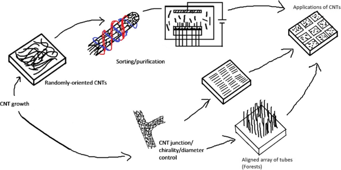
论文的示意图。在这篇综述中,讨论了控制从单个管(即手性、结和直径)到各种纯化、组装、排列技术和大量纳米管集成以用于广泛应用的 CNT 组装和集成的进展
控制单个 CNT
CNT 增长—概览
制造碳纳米管最广为人知的技术是电弧放电、激光烧蚀和化学气相沉积。通过利用电流(在电弧放电中)、高强度激光(在激光烧蚀中)和热量(在 CVD 中)的方法释放导致形成 CNT 的碳原子。以下部分将简要讨论这些技术。
电弧放电
碳纳米管是使用电弧放电法从石墨电极的碳烟灰生产的 [78]。电弧放电法采用高温(超过 1700 °C)合成碳纳米管。该方法由两个石墨电极、一个阳极和阴极(直径分别为 6 毫米和 9 毫米)组成,它们在大型金属反应器中相距约 1 毫米,如图 5 [79] 所示。在金属反应器内保持惰性气体处于恒定高压的同时,施加 ~ 100 A 的直流电和 ~ 18 V 的电位差 [80]。当两个电极靠近时,会发生放电,从而形成等离子体。在较大的电极上形成含有纳米管的碳质沉积物。碳黑形式的多壁碳纳米管,内径为 1 纳米至 3 纳米;观察到~ 2 nm 至 25 nm 外径沉积在负极中 [1, 78]。通过用钴 (Co)、铁 (Fe) 或镍 (Ni) 等金属催化剂掺杂阳极,并使用纯石墨电极作为阴极,SWCNT 可以生长到大约 2 nm 至 7 nm 的直径 [81 ,82,83]。该技术可用于生长大量 SW/MWCNT。然而,该技术的主要缺点是产量有限,因为使用金属催化剂会引入不需要的需要纯化的反应后产物。
<图片>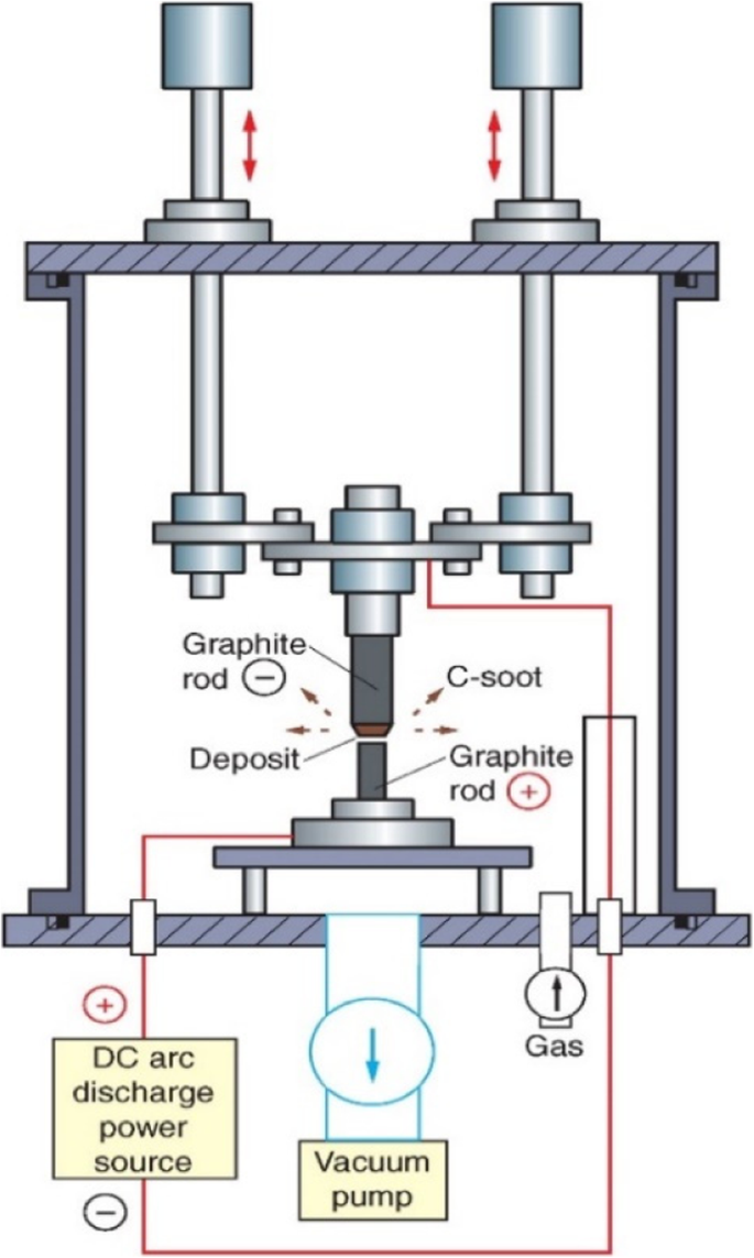
用于合成碳纳米管的电弧放电系统示意图。在这种技术中,当大电弧电流在保持高压和高温的金属反应器内流动时,在其中一个石墨电极上产生纳米管。改编自 [79]
激光烧蚀
这种技术类似于电弧放电技术;然而,它采用连续激光束或脉冲激光,如图 6 [84] 所示,而不是电弧放电。激光束在惰性气体(如 He、Ar、N2 等)的存在下,在约 1200 °C 的石英管式炉中蒸发大石墨靶。然后,蒸发的碳冷凝,碳纳米管在反应器较冷的表面自组装 [85,86,87,88]。如果两个电极均由纯石墨制成,则生成的 MWCNT 内径约为 1 nm 至 2 nm,外径约为 10 nm [89]。当石墨靶掺杂 Co、Fe 或 Ni 时,观察到所得沉积物富含 SWCNT“绳”或束(图 1e)。所生产的碳纳米管的产量和质量取决于生长环境,例如激光特性、催化剂组成、生长温度、气体和压力的选择。由于需要高功率激光束,这种方法可能很昂贵。这种技术的一个优点是由于杂质较少,生长后纯化不像电弧放电法那样密集。
<图片>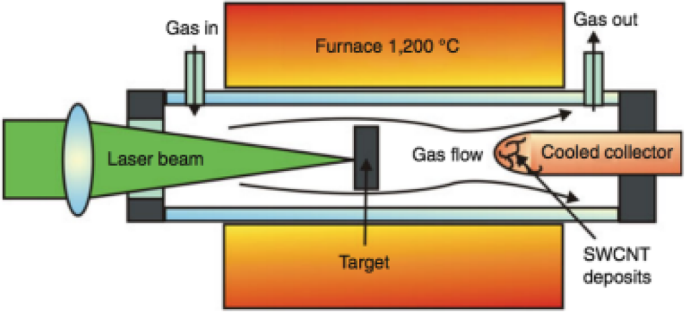
用于合成碳纳米管的激光烧蚀系统示意图。在这项技术中,碳纳米管是在石英管式炉中在激光束的帮助下生产的,该激光束使石墨靶蒸发,导致碳纳米管在反应器表面自组装。根据电极的类型(纯石墨或掺杂 Co、Fe 或 Ni 的石墨),形成的 CNT 可以是单壁或多壁的。改编自 [84]
化学气相沉积
由于在烃蒸气的热分解中使用金属催化剂,因此化学气相沉积 (CVD) 通常被称为催化化学气相沉积 (c-CVD)。催化剂在碳纳米管的生长中起着非常重要的作用。理想的催化剂应单分散在基材表面。它还应该通过范德华力与基材适当地相互作用。当催化剂和基材之间存在弱相互作用时,可以提高 SWCNT 的生长效率。在高温下,金属催化剂非常不稳定,单壁碳纳米管的手性控制生长成为一项具有挑战性的任务。理想的催化剂应在较高温度下提供良好的稳定性,并导致具有更好直径分布的 CNT 可控生长。通过增加催化剂载体和催化剂纳米颗粒之间的相互作用,可以实现对高温下遇到的一些问题的控制。烃源可以是液体(苯和酒精)、蒸气(一氧化碳)或固体形式(樟脑)[79]。对于碳氢化合物的分解,通常使用纳米尺寸的过渡金属催化剂,如 Fe、Co、Ni、Mo [90,91,92]。此外,一些研究中也使用了铜、金、银和铂等金属催化剂[93]。在某些情况下,这些金属催化剂与催化剂载体如 SiO2、MgO 和 Al2O3 混合,以增加涉及碳原料和金属颗粒的催化反应的表面积 [94]。
所用碳氢化合物和催化剂类型的选择决定了各种生长机制,称为气-液-固 (VLS) 或气-固-固 (VSS) 机制。两者中,VLS机制被广泛使用。此处,催化剂颗粒处于液相,其中烃类吸附在金属颗粒上并被催化分解。接下来,碳通过溶解到颗粒中形成液体共晶,然后在过饱和时沉淀成管状形式 [95, 96]。另一方面,VSS的生长机制使用固体催化剂[97]。
合成方法开始于在金属催化剂存在下在 ~ 600–1200 °C 的温度下分解烃蒸气 [98, 99]。当烃蒸气与金属相互作用时,它分解成碳和氢。当氢气蒸发时,碳溶解到金属中。然后,基于催化剂 - 基材的相互作用,碳纳米管在金属催化剂上的生长要么是尖端生长机制,要么是碱生长机制 [100, 101],如图 7 所示。 尖端生长机制是由于弱催化剂-底物相互作用。在这里,碳氢化合物在金属顶部分解,而碳开始通过金属扩散。碳纳米管从金属底部开始生长,并继续生长更长的时间,直到根据金属的浓度梯度有足够的空间进行额外的碳氢化合物分解。在这个过程中,金属被推离基板更远,如图 7a 所示。在碱增长机制的情况下,存在强烈的催化剂 - 底物相互作用。类似于尖端生长机制,碳氢化合物在金属顶部分解,而碳开始通过金属扩散。然而,由于强烈的催化剂 - 基材相互作用,金属颗粒没有被推得更高,并且 CNT 在金属顶部生长,如图 7b 所示。图 8 显示了通过 CVD 生长的碳纳米管的例子 [102, 103]。
<图片>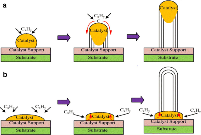
使用 CVD 的 CNT 的不同生长机制(改编自 [101])。基于催化剂-基材的相互作用,可以看到两种类型的 CNT 生长机制。 一 尖端生长模型:在催化剂-基材相互作用较弱的情况下,观察到尖端生长,其中碳氢化合物在金属顶面分解,导致碳向下扩散穿过金属,导致碳纳米管从金属底部生长。 b Base-growth模型:由于催化剂-基材相互作用强,观察到碳纳米管从远离基材的金属中生长出来而催化剂扎根于基体的基础生长
<图片>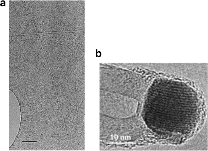
通过 CVD 生长的 CNT 的 TEM 图像 (a ) 使用 Fe2O3 催化剂生长的直径为 5 nm 的孤立 SWCNT。比例尺等于 50 nm。改编自 [102]。 b MWCNTs 在末端用催化剂颗粒生长。改编自 [103]
Size and properties of the catalyst play a significant role in the growth of SWCNTs and MWCNTs using CVD. Smaller particle size (a few nm) leads to the growth of SWCNTs, whereas MWCNTs are formed when the particle size is larger (tens of nm) [1]. The type of hydrocarbons influences the shape of the CNTs produced. For example, methane, acetylene which are linear hydrocarbons, lead to formation of straight hollow CNTs. Cyclic hydrocarbons like benzene and fullerene produce curved CNTs [104].
In addition, the choice of substrate used also plays an important role in the growth of CNTs due to the catalyst–substrate interactions, in turn influencing the yield, quality and aspect ratio of the CNTs produced. Some of the commonly used substrates for growth of CNTs are made of materials like silicon [104], graphite [18], alumina [105, 106] and zeolite [107]. Studies have shown that use of zeolite substrates can result in high yields with narrow diameter distribution and that substrates made of alumina produce high yields of aligned CNTs with high aspect ratio [79, 108].
Along with the catalyst and substrate choices, structural control of individual CNTs is also affected by the temperature and the gas flow rate during the synthesis procedure. Control of gas flow rate during synthesis depends on the type of hydrocarbons used (i.e. gaseous, solid or liquid. An increase in the SW/MWCNT’s diameter is observed with an increase in the synthesis temperature [109]. For example, in case of a Fe–Co–zeolite system with camphor, the ideal temperature for SWCNT growth was reported to be around 900 °C, whereas for MWCNTs, the ideal growth temperature was reported to be 650 °C [100].
Of the three CNT manufacturing techniques discussed in this section, CVD is a widely used technique to manufacture CNTs due to its various advantages such as better controllability over CNT growth, low cost and use of low temperature [79, 105].
Structural Control of Individual CNTs
Chirality Control
Growing CNTs with controllable chirality is an important step in order to utilize them for various applications. This is because the chirality of a CNT determines various properties like electronic band structure and thus, the type of CNTs grown (i.e. metallic vs. semiconducting). Chirality control can be done by direct-controlled growth or post-synthesis separation approaches or by combining these methods [110] and is considered as one of the most challenging aspects in CNT growth [111]. Various parameters such as growth temperature, catalyst and hydrocarbon type influence the chirality of the CNTs. Direct controlled growth methods aim at controlling the chirality by controlling the nucleation process, as it is reported that during the nucleation process, chirality of a SWCNT is fixed [112]. For example, plasma-enhanced CVD (PECVD) has been used for the preferential growth of semiconducting SWCNTs [113]. In addition, semiconducting CNTs were also grown using ST-quartz substrates and methanol precursors [114]. Various growth parameters like type of catalyst, growth temperature and pressure and the source of the hydrocarbons play a significant role in influencing the nucleation which in turn controls the chirality of the tubes grown. Some of the techniques like use of CNT growth templates as seeds (both metal-based and non-metal based), growth initiated by carbon molecular-based precursors and use of nanoparticle-based catalysts have gained a great interest in this field. Some of these are discussed below:
In the first technique we describe, a single (n , m )-type SWCNT nanotube sample is cut into smaller pieces (seeds), each of which was aimed to be used as a template for the growth of a longer nanotube using a VLS amplification process (Fig. 9a). The main goal of this method was to grow large quantities of n , m -controlled structures. Each seed was polymer-wrapped SWCNT, end-carboxylated and tethered with Fe salts at its ends. During the growth process, Fe salts acted as growth catalysts and use of VLS mechanism aimed at achieving narrow diameter distribution [115]. SWCNTs grown with this method had a diameter similar to the diameter of the growth seed (Fig. 9b–f). However, details about the modifications in chirality of the tubes grown could not be clearly established [116]. In addition, this method also involves the need for complex purification steps due to the presence of metallic particles in the SWCNTs grown, thus affecting the final product’s quality.

一 Growth mechanism of SWCNTs using Fe seeds as growth templates. Adapted from [116]. b , c Atomic force microscope (AFM) images and height analysis of SWCNTs before the amplification process. Adapted from [116] and d , f after amplification growth process. Adapted from [116]. White arrows represent the original SWCNT seed location, red arrow indicates the seed position and angle relative to the locator inscription and yellow arrows show the entire length of the amplified nanotube. Adapted from [116]
As an alternative to metal-catalyst-based growth, another technique involved the controlled growth of CNTs by using semiconductor nanoparticles like Si and Ge as the growth templates. In one of these experiments, CNTs were grown using semiconducting nanoparticles (of size 5 nm or smaller), by introducing thermally decomposed carbon atoms from ethanol at 850 °C. However, CNTs grown in this experiment were considered to be of very low quality and low yield as compared to experiments using Fe, Co or Ni as catalysts [117]. Another growth technique was via an open-end growth mechanism, commonly referred as ‘cloning’ (Fig. 10) [118]. Here, the chirality of the SWCNTs was controlled by using open-end SWCNTs as seeds/catalysts without using a separate metal catalyst. Using these seeds, duplicate CNTs were grown on a SiO2/Si substrate. The total yield reported in this method was ~ 9%, which could be improved to 40% by growing SWCNTs using this method on a quartz substrate [118]. Another technique based on vapor-phase epitaxy was used to grow the SWCNTs with predefined chirality. This method combined CVD and SWCNT separation techniques by using deoxyribonucleic acid (DNA)-separated single chirality SWCNT seeds as the growth templates. These seeds were of very high purity (~ 90%) and C2H5OH and CH4 were used as the carbon sources. This experiment showed significant elongation of the SWCNTs grown from a few 100 nm to tens of microns. The total yield produced in this method was very low [110] and some of the studies related to vapor phase epitaxy (VPE)-based growth techniques are ongoing with aims to improve the yield.

一 –c Schematic diagram showing the growth process of ultra-long SWCNTs using e-beam lithography cut nanotube segments as the template via ‘cloning’ mechanism. Adapted from [118]. d , e SEM and AFM images SWCNTs used for preparing open-end SWCNTs seeds. Adapted from [118]. f , g SEM and AFM images of short parent SWCNTs segments for the second growth Adapted from [118]. h , i SEM and AFM images of duplicate SWCNTs continued grown from the SWCNTs. Adapted from [118]
One way to selectively grow chiral SWCNTs is by using silica substrate and Co-Mo catalyst [119]. Nanotubes of (6,5) and (7,5) chirality were obtained in this technique. With proper interaction between the Co and Mo oxides, aggregation of Co nanoparticles at high temperatures could be avoided. In addition, by optimizing the gaseous feed composition, growth and temperature, selectivity of (6,5) nanotubes was improved by ~ 55% [120]. Another approach for the selective growth of (6,5) SWCNTs was demonstrated using Co-Si catalyst and provided narrow distribution chiral SWCNTs [121]. High quality (6,5) tubes have also been grown at 800 °C using atmospheric pressure alcohol CVD on silica-bimetallic CoPt catalysts with narrow chirality distribution by tailoring the catalyst composition [122]. (9,8) SWCNTs were grown with high selectivity using Co nanoparticles and nanoporous Si support (TUD-1) [123]. Recently, (12,6) SWCNTs were synthesized using tungsten-based bimetallic solid alloy catalyst, W6Co7, with purity of> 92% (Fig. 11) [124]. This high level of purity was attributed to the W6Co7 catalyst which has a very high melting point of 2400 °C and provides a potential avenue for the growth of high purity SWCNTs by using nanoparticle catalysts.

Growth of high purity, single chirality (12,6) SWCNTs using tungsten-based bimetallic solid alloy catalyst (W6Co7). These alloy nanoparticles catalyze the CNT growth on SiO2/Si substrates via ethanol CVD that help in chirality control during CNT growth. Adapted from [124]
Recently, selective growth of semiconducting SWCNT with diameters in the range of 0.8–1.2 nm was reported based on the deactivation process of the catalyst using a technique known as ‘catalyst conditioning process’ [125]. Here, the catalysts favoring the growth of metallic SWCNT are exposed to the catalyst conditioning parameters (oxidative, i.e. water) and reductive (i.e. H2) gases prior to the growth process which leads to the deactivation of these catalysts. An inverse relationship between yield and selectivity based on catalyst deactivation was reported in this work.
Evolving methodologies in the field of organic chemistry have enabled the synthesis of various carbon-based precursors that could be used in growing CNTs with controlled chirality. Some of the examples include flat CNT end-caps, three-dimensional CNT end-caps and carbon nanorings [111, 126, 127], which have all been tested and have proved to stimulate CNT growth under controlled environment. However, each of these approaches has some limitations [128].
In one method, in order to yield hemispherical caps, thermal oxidation was used to open fullerndione. However, there were challenges in the synthesis of single chirality CNTs due to the lack of control in the formed hemispherical cap structures [129]. Synthesis of CNTs using carbon nanorings, viewed as sidewall segments without the cap was also developed [126] but the researchers were unable to control the chirality of the as-grown CNT. An alternative technique was developed by other researchers using an organic chemistry approach to synthesize pure molecular seeds of C50H10 as an end-cap of a (5,5) chirality nanotube [130]. In this method, the researchers demonstrated chirality-controlled synthesis of SWCNTs through VPE elongation that was free of metals (Fig. 12a). Even though the grown nanotubes were well aligned and of high density, in Raman characterization, it was observed that the synthesized SWCNTs were not (5,5) chirality. It was also observed that the as-grown semiconducting nanotubes were of smaller diameters [130]. Around the same time, another method was demonstrated to synthesize single chirality SWCNTs with predetermined chirality by using an end-cap precursor and planar single-crystal metal surface [131]. In this method, the researcher’s custom synthesized a precursor (C96, H54) using organic chemistry approach to yield (6,6) nanotube seed through surface-catalyzed cyclodehydrogenation process (Fig. 12b). Although, Raman characterization using 532 nm laser identified that the synthesized SWCNTs had (6,6) chirality, some researchers argue that 532 nm is not in resonance with (6,6) nanotubes. In their study, they quoted that 532 nm was in resonance with (9,2) or (10,0) chirality nanotubes. Furthermore, few others observed that the splitting of G band is not consistent with initial studies in this area that demonstrated the G band of armchair metallic nanotubes as a single symmetric peak [132, 133]. The researchers have recommended further Raman characterization, STM studies to determine whether the as-grown SWCNTs are of (6,6) chirality. The use of organic chemistry techniques has the potential to be referenced in further development of chirality controlled SWCNT synthesis due to the possibility of large-scale synthesis with higher purity.

一 Structure molecular end-caps used for chirality controlled synthesis of (5,5) SWCNTs through VPE elongation that was free of metals. Adapted from [130]. b Schematic illustration of a two-step bottom-up synthesis of SWCNTs from molecular end-cap precursors. Singly capped ultrashort (6,6) seeds lead to epitaxial elongation of nanotubes using the carbon atoms originating from the surface-catalysed decomposition of a carbon feedstock gas. Adapted from [110]
Most of the fabrication methods used to grow SWCNTs produce polydisperse CNTs of metallic, semi-metallic and semiconducting properties. This variation is based on the way the graphene sheet is wrapped, denoted by the indices (n, m ) that define the chirality of the tube grown. Steps to control these variations are essential for various applications of SWCNTs as the presence of multiple conductivity types can hinder the device performance. Some of the earlier techniques involved the use of gas-phase etchants like methane plasma [134], water vapor [135], oxygen [136, 129, 137] and hydrogen [134], that would etch metallic particles during the synthesis due to their higher reactivity with the metallic nanotubes, thereby leaving the semiconducting nanotubes behind.
Using floating catalyst chemical vapor deposition (FCCVD) technique with oxygen as an etchant in selective removal of m-SWCNTs, ~ 90% yield containing s-SWCNTs with diameters 1.4–1.8 nm were obtained [137]. However, oxygen can combine with other carbon-based materials due to its strong oxidizing properties during the growth process. Controlling the concentration of oxygen during the growth process is a challenging task. As an alternative, water vapor can be used as an etchant in the CVD technique, as it has a much weaker oxidizing ability. A yield of ~ 97% was reported with this technique [138].
Recent studies have reported the importance of diameter dependence on the etching mechanisms. In one of the studies, m-SWCNTs were selectively etched using methane plasma, followed by annealing. At the end, s-SWCNTs are retained on the growth substrates which were stable at high temperatures [139]. By narrowing the diameter distribution to an optimal range of SWCNT diameter, most of the m-SWCNTs are etched within this range. In another technique, to control the diameter distribution, bimetallic solid alloy catalysts like Fe–W (Iron-tungsten) nanoclusters were used as catalyst precursors due to high-temperature stability of tungsten, which causes the nanoclusters to be stable during the CVD synthesis. Water vapor was used as an etchant during the growth process. A yield of ~ 95% was reported with this technique and the diameter of about 90% of the s-SWCNTs formed on the quartz substrate was reported to be in the range of 2–3.4 nm as shown in Fig. 13 [140]. A similar experiment using Fe nanoparticles as catalysts was performed where the overall yields showed broad distribution of the catalyst particle size due to mobility of Fe nanoparticles, which are usually in liquid state during high-temperature CVD growth [94].

一 Diameter and chirality distributions of the FeW-catalysed SWCNTs under a water vapor concentration of 522 ppm. About 90% of the as-prepared SWCNTs were reported to be in the diameter range of 2.0–3.2 nm adapted from [140]. b Schematic illustration of the diameter-dependent and electronic-type-dependent etching mechanisms during growth. High selectivity of s-SWNTs could be obtained by controlling the diameter via the Fe-W catalysts. Adapted from [140]
Another technique to grow s-SWCNTs with narrow diameter distribution is using carbon-coated cobalt nanoparticle catalyst (termed as acorn-like catalyst) as shown in Fig. 14. The Co nanoparticle acts as active catalytic phase for SWCNT growth. Carbon coating on the outer end prevents aggregation of Co nanoparticles, a major problem faced by most growth methods that lead to formation of larger particles during SWCNT growth at high temperatures [141]. In this technique, the yield of s-SWCNTs grown was ~ 95% with a very narrow diameter distribution centered at 1.7 nm [138].

Step-by-step description of growth of s-SWCNTs with narrow diameter distribution using carbon-coated Co nanoparticle catalysts. Solvent annealing, use of air plasma followed by thermal treatment produced a yield of ~ 95% s-SWCNTs with diameters of about 1.7 nm. 一 Poly-(styrene-block-4-vinylpyridine) film self-assembled into vertical nanocylinders. b Formation of phase-separated nanodomains from the vertical nanocylinders and adsorption of K3[Co(CN)6]3 catalysts onto them. c CoO nanoclusters partially surrounded by a polymer layer. d Co catalyst nanoparticles partially coated with carbon to produce acorn-like bicomponent catalysts. e Growth of SWCNTs with a narrow diameter distribution from the partially carbon-coated Co nanoparticles followed by in situ etching of m-SWCNTs. f s-SWCNTs with a narrow band-gap distribution. Adapted from [138]
Controlling CNT Geometry
Diameter
Growth of SWCNTs with controllable diameters is regarded as one of the critical parameters in influencing its electrical, surface functionalization and thermal properties [1]. Properties such as band gap and chirality can be controlled by variations in the diameter of the SWCNTs formed. SWCNTs diameter control may be via their growth using floating catalyst method or from a substrate growth method with catalysts deposited on top or using template growth approach. Of the first two techniques, growth via floating catalyst method offers better control over the diameters of the tubes grown due to limited aggregation as catalysts are not restricted on a single plane of the substrate. Studies have shown diameter control in the range of ~ 1.2 to 2.1 nm using this method [126]. In one of the studies, diameter control was achieved by adding CO2 (which acts as an etching agent to etch tubes with small diameters) with the carbon source into the aerosol CVD reactor. The corresponding transmission electron microscope (TEM) image and the absorption vs. wavelength plot of SWCNTs grown with different CO2 concentrations is shown in Fig. 15 below. Increasing the concentration of CO2 leads to the shift in SWCNT diameters from 1.2 to 1.9 nm [142] as shown in Fig. 15c. Size and properties of the catalyst also play a significant role in the controlling the growth of SWCNTs and MWCNTs. Smaller particle size (a few nm) leads to the growth of SWCNTs, whereas MWCNTs are formed when the particle size is larger (tens of nm) [143]. For example, with Fe catalyst of average diameters of 9 and 13 nm, MWCNTs of average diameter 7 and 12 nm were produced [105].

一 TEM image of SWCNTs grown by adding CO2 along with carbon source. (Inset) shows the TEM image of an individual SWCNT Adapted from [142]. b Plot showing the absorption vs wavelength of SWCNTs grown with different CO2 concentrations. Adapted from [142]. c The corresponding diameter distributions of SWCNT samples with different CO2 concentrations. Adapted from [142]
Substrate growth method aims at minimizing particle aggregation by increasing catalyst spacing. For example, centrifuging the nanoparticles before deposition via CVD using ferritin catalyst particles leads to a diameter control in the range of. 1.9 to 2.4 nm [144]. Alternatively, by sandwiching Fe between Al2O3 in a sandwiched catalyst model, SWCNTs with diameters between 0.8 to 1.4 nm were synthesized [145]. However, SWCNTs grown using these techniques were entangled due to large catalyst spacing.
Another way of controlling the diameters of SWCNTs is by using a template-based growth approach [126, 146,147,148]. Use of carbon nanorings (cycloparaphenylenes), representing the shortest sidewall segment of armchair CNTs (Fig. 16) as growth templates and ethanol as a hydrocarbon source, SWCNTs with diameters in the range of 1.2–2.2 nm were grown. Different types of nanorings (based on number of benzene rings in the structure) were used as growth templates. The diameters of SWCNTs grown were similar to the diameter of the carbon nanorings used, thereby providing an avenue for diameter control of SWCNTs using organic chemistry approaches.

一 Schematic of template-based CNT growth using carbon nanorings (cycloparaphenylene) that represent the shortest sidewall segment of armchair CNTs. Adapted from [126]. b Representation of various carbon nanorings grown using the template-based method and their corresponding diameters in nm. Adapted from [126]
Several methods report the growth of MWCNTs with controlled diameters [149,150,151,152,153,154]. In one of the methods, aligned CNTs with diameters in the range of 20–400 nm and lengths between 0.1 and 50 μm were produced using the plasma-enhanced hot filament CVD method by tuning the catalyst size (Fig. 17a). Another method reported the importance of supply of carbon reactant and the growth temperature in the formation of large diameter nanotubes [105]. Here, the use of an iron nanocluster with diameter of 9 nm, ethylene as the carbon reactant and growth temperature of 900 °C, large diameter nanotubes with two or three walls were produced. Alternatively, arrays of SWCNTs with diameters of ~ 1.5 nm were obtained using lithographically patterned metallic nanoclusters (Fig. 17b).

CVD based growth of CNTs produced using different diameter nanoparticle catalyst. 一 SEM images of CNTs produced with different diameters (250 nm and 20 nm in diameter) using nickel-coated glass substrates. Adapted from [149]. b AFM images of nanotubes grown using lithographically patterned catalyst and Co nanoparticles with a diameter of ∼ 1.7 nm. Adapted from [150]
Junctions
Modifications in the growth of CNTs leading to junction-like formations can create nanotube structures like the three-terminal Y-junction that could be used for novel electronic switching devices and transistors [155,156,157,158]. Y-junction nanotubes can be grown by CVD using anodic alumina templates with adjustable stem and branch templates [159, 160] as shown in Fig. 18a. Another method used Ti-doped Fe catalysts in the growth process to produce MWCNTs (~ 90%) branched in the form of a Y-shaped junction on quartz substrates (Fig. 18b) [161].

一 TEM image of a MWCNT Y-junction nanotube grown by CVD using branched nanochannel anodic alumina templates. The grown Y-junctions were reported to be 6 to 10 μm in length with tunable diameters. Adapted from [159]. b TEM image of MWCNT Y-junction nanotube grown using Ti-doped Fe catalysts. Catalyst present at the junction (shown as A) leads to the formation of the two branches. B shows a Y-junction grown from catalyst particles that attach on the walls of the nanotube. C represents a catalyst nanoparticle that does not lead to further branching. Adapted from [161]
In addition to the above techniques, SWCNT junctions formed via crossing of different CNTs connected via irradiating the junction with electron beam, using scanning electron microscopy (SEM) have also been reported [162, 163]. Here, under the influence of electron beam, hydrocarbons used in the growth process are transformed into amorphous carbon which is then utilized to attach the nanotubes and form mechanical junctions (Fig. 19a, b). In another similar work, various carbon nanotube junctions (Y-, T-shaped) were formed by electron beam welding which induced structural defects in the nanotubes, leading to the joining of tubes by cross-linking of dangling bonds (Fig. 19c, d) [162].

Growth of a MWCNT nanotube junction (a ) before and (b ) after soldering by deposition of amorphous carbon via electron beam irradiation. Adapted from [163]. c Y-shaped junction formed by electron beam irradiation. Adapted from [162]. d T-shaped nanotube junction formed after irradiating a preformed Y junction. Adapted from [162]
Alternatively, two-terminal SWCNT junctions can be grown in a controlled manner using temperature modulation during the CVD process (Fig. 20) [141]. In this method, by altering the growth temperature, systematic variations in the diameter and chirality of the SWCNTs lead to the formation of SWCNT intramolecular junctions. These junctions were grown at desired locations by increasing the temperature of the substrate locally using infrared light during CVD. It was also observed that increasing the temperature led to a decrease in the diameter of the growing junctions and vice versa, with no change in the catalyst particle present at the growing tip [141].

一 SEM image of a two-terminal SWCNT intramolecular junction formed by varying the temperature during CVD growth from 950 to 900 °C (temperatures are indicated by T1 and T2). Adapted from [141]. b The corresponding shift in the Raman spectra with variations in the temperature. Inset shows the schematic illustrations of SWNT diameter variations with temperature. Adapted from [141]
Post-Growth Purification/Sorting of Single Tubes
Understanding CNT sorting methodologies is important as many of the advanced applications, such as FETs and nanoscale sensors, require monodispersed samples with little structural variation [164]. Before CNT sorting can take place, the tubes must be dispersed in a liquid medium (water or organic solvents). Unfortunately, there are certain constraints which may prevent separation in an aqueous dispersion. For example, CNTs have very strong Van der Waals interactions which restrict sorting [87]. There are several well-developed techniques currently being used for the post-growth purification or sorting of tubes. Some of these are discussed below.
One of the techniques, commonly referred to as the density gradient ultracentrifugation (DGU), has been shown to produce a high yield of pure SWCNTs, without much need for chemical treatment of the sample [165, 166]. DGU, which depends entirely on the buoyant density of the CNT, is an isopycnic separation process. The process is achieved by wrapping the SWCNT sample with a surfactant (Fig. 21) [166]. After the grown SWCNTs are mixed with the surfactant, the aqueous dispersion of surfactant-encapsulated tubes is added to the centrifuge tubes, which contains a pre-existing density gradient medium. A strong centrifugal force is then applied, and it causes the surfactant-wrapped SWCNTs to be separated by the movement of SWCNTs to regions of the density gradient medium which match the tubes’ buoyant densities (isopycnic points). The aqueous dispersions of the SWCNTs are produced by using either linear chain surfactants or bile salts. The density gradient medium is usually made of a salt (lithium chloride, cesium chloride, sodium chloride) solution in water. Nonlinear gradients are preferred because they are very sensitive and allow trapping of particles over the entire length of the centrifugal cell. The gradient density and its variation are important to the sorting process wherein, the gradient needs to be set up such that the distance between the tubes and their isopycnic points is minimal. As the density gradient medium responds to the centrifugal force, it leads to steeper gradient over time and hence redistribution of the density profile takes place during centrifugation [167]. After the centrifugation process, the sorted SWCNTS are removed layer by layer using the fractionation process (using piston, upward and downward fractionation methods), which involves extracting quantities of mixtures to different aliquots which vary in composition with respect to the density gradient of the original mixture. Uniform surfactant coverage is important or adsorbed surfactant molecules will begin to aggregate and form clusters along the tube sidewalls, thereby impeding effecting separation of the tubes. To separate metallic and semiconducting tubes, a co-surfactants mixture is used for the ultracentrifugation process. After the semiconducting tubes have been separated, chirality enrichment of tubes is carried out to generate samples that are rich in a certain chirality of tubes, and the resulting semiconducting-SWCNTs-enriched fraction is passed through a dialysis membrane to remove the surfactants from the SWCNT sidewalls [168]. Finally, the tubes are characterized using various optical spectroscopy methods.

一 Illustration of DGU separation of tubes coated with surfactant based on their diameter and metallicity. The near infrared absorption spectra of SWCNTs is also shown. Adapted from [166]. b Clear separation of SWCNTs by electronic type and the corresponding absorbance spectra for semiconducting SWCNTs (in red) and metallic SWCNTs (in blue) is shown. Adapted from [166]
Another separation technique, referred to as the ion-exchange chromatography (IEX), is based on the ion-exchange processes occurring between a mobile phase and stationary ion-exchange groups (which are bonded to the support material). The IEX separation method is carried out on single-stranded-DNA-wrapped (ssDNA) SWCNTs, which have different electrostatic interactions with an ion exchange column [169, 170]. By selecting the desired sequence from the vast ssDNA library, purification of the specific (n, m) species was possible. With certain ssDNA sequences greatly improving separations between metallic and semiconducting CNTs as well as between semiconducting CNTs of different diameters and electronic band gaps [171]. The IEX process begins by wrapping ssDNA around individual SWCNTs, to form DNA/CNT hybrids. Some of the DNA/CNT hybrids in aqueous dispersions are electrostatically bound to the positively charged anion-exchange resin (stationary phase). As the mobile phase is passed over the hybrid-resin system, and its ionic strength increases, hybrids with the lowest effective charge density elute within the shortest IEX times. Because the hybrids are found in both the stationary and mobile phases, the separation is based on differences in this distribution. There is less electrostatic attraction between metallic hybrids and the IEX resin than between semiconducting hybrids and the IEX resin, thus in a mixture of metallic and semiconducting CNTs of the same diameter, the metallic hybrid will elute from the column first. This method of DNA-wrapped CNTs produced many single-chirality semiconducting CNTs. Figure 22a shows the optical absorption spectra of 12 purified semiconducting SWCNTs along with their structure. This method could also be used for purification of armchair metallic tubes [133, 169]. An alternative approach to sort metallic and semiconducting CNTs is using anion-exchange chromatography technique. Here, single-stranded DNA form stable complexes with CNTs and can effectively disperse them in water. Here, the chosen DNA sequence self-assembles into an ordered structure around an individual nanotube, helping in nanotube formation (Fig. 22b).

Purification of CNTs with defined helicity with the aid of specific DNA sequences using IEX. 一 Absorption spectra of twelve purified semiconducting CNT species along with their (n, m ) structural notations. Adapted from [169]. b Molecular dynamics model of (8,4) nanotube obtained by rolling a 2D DNA sheet with ATTTATTTATTT strands. Orange color indicates thymine, green color indicates adenine and yellow color shows the backbones. Adapted from [169]. c , d Chirality separation of SWCNTs using allyl-dextran-based multi-column chromatography. c Using SDS as a single surfactant, the dispersed SWCNTs were adsorbed on column medium and, upon saturation, the single-chirality tubes are enriched according to its binding affinity towards the column. Adapted from [176]. d Bulk separation of iterative column chromatography to produce single chirality enriched SWCNTs, showing their distinct colors according to their chirality. Adapted from [176]
Gel chromatography, particularly, agarose gel chromatography is a method of separating semiconducting CNTs from metallic CNTs in an mass-spectroscopy mixture using hydrogels [172, 173]. Agarose gel beads are used for mass-spectroscopy separation, owing to their simplicity, affordability, short process time of about 20 min and scalability. The mechanism for gel chromatography follows a few simple steps. First, the SWCNT mixture, containing both metallic and semiconducting CNTs, would be dispersed in an aqueous surfactant solution, such as sodium dodecyl sulfate (SDS). The wrapping and encapsulation of the SDS surfactant molecules around SWCNTs plays a crucial role in the separation mechanism. The interaction between SDS molecules and SWCNTs via ion-dipole forces depends on the pH condition and concentration of SDS molecules. Due to the electrostatic properties of SWCNTs [174], SDS molecules form different types of micellar structures around semiconducting and metallic SWCNTs [172, 175]. On semiconducting CNTs, randomly oriented, flat micellar structures are formed, while for the metallic CNTs, cylindrical micellar structures are formed. This is mainly due to difference in ion-dipole forces between metallic and semiconducting CNTs during their adsorption on agarose gel. These disparate encapsulation mechanisms form the basis of the separation process. After the SWCNT dispersions are formed, they are ultra-centrifuged to remove SWCNT bundles and other impurities, and the SWCNT-surfactant solution is pipetted to be used in the separation process. Next, a separating column is filled with agarose micro-beads suspended in ethanol, after which the column is washed and equilibrated using the surfactant aqueous solution. The agarose-SWCNTs mixture, which is to be separated, is then poured into the column, and the SDS solution is added. This causes a displacement of the SWCNT dispersion along the column. A portion of the SWCNTs (the semiconducting CNTs) are trapped at the top layer of the agarose beads, while the metallic CNTs move to the bottom of column. This movement is related to the encapsulation of the tubes. Because semiconducting SWCNTs are encapsulated by flat randomly oriented SDS micelles, and have less surfactant coverage, there will be an ineffective shielding between the semiconducting SWCNTs and the agarose gel, and thus, a stronger affinity of the semiconducting SWCNTs to the gel. However, the metallic SWCNT walls are surrounded by an ordered high-density cylindrical micellar structure, which causes a steric hindrance between the SWCNTs and the agarose gel. Therefore, the metallic tubes have less affinity to the agarose gel. A schematic of SWCNTs separation based on the chirality of the tubes is shown in Fig. 22c, d [176].
Another technique to separate metal and semiconductor nanotubes is using the technique of dielectrophoresis (DEP). When a particle is placed in an electric field, a lateral force, also known as a dielectric force acts on it [177]. This force can be used to manipulate nanoparticles or cause them to move, and the resulting movement of particles is termed dielectrophoresis [178]. The operating principle of the alternating current (AC) DEP process is based on the fact that metallic and semiconducting CNTs have different dielectric constants. The setup consists of a fabricated microelectrode, fluidic chamber and the SWCNT solution. The DEP force is generated by applying a non-uniform electric field to the setup. Due to the applied electric field, a dipole moment is induced on the SWCNT mixture, and the tubes will move towards the maxima or minima of the electric field depending on their polarity. Under the action of an AC electric field, CNTs in solution will move to the electrodes depending on their surface charge [179,180,181]. The electrodes are typically fabricated using e-beam lithography, which are then attached to a function generator. When an AC electric field originating from the function generator operating at 20 V peak-to-peak voltage and a frequency of 10 MHz is applied, a suspension of ~ 10 μL of SWCNTs is deposited. The metallic nanotubes will attach themselves to the electrodes, while the semiconducting tubes will remain in the suspension (Fig. 23) [182]. This is due to the divergent responses of the different types of CNTs to the electric field. In this technique, direct current (DC) electric field is not usually used as it leads to aggregation of CNTs near one of the electrodes [179]. The applied electric field and deposition time are the crucial parameters which control the CNT deposition yield.

一 Schematic of the experimental setup of the dielectrophoresis of a SWCNT solution using a microelectrode array. The metallic tubes (in black) are deposited on the electrodes and semiconducting tubes are left in suspension (in white). Adapted from [182]. b Rayleigh scattered dark-field micrograph showing aligned SWCNTs (in green) and the corresponding polarized SWCNTs perpendicular to the electrodes. Adapted from [182]
Gel electrophoresis was developed as an improvement to the AC dielectrophoresis method. This process makes use of the same mechanism as AC electrophoresis but uses agarose gel as a medium. SWCNTs dispersed in an aqueous SDS surfactant are used to fill a gel column and subjected to an electric field. This causes a movement of the m-SWCNTs through the gel medium to the anode while the s-SWCNTs are adsorbed to the gel [177, 178].
Sorting of CNTs can also be done using solution-based conjugated polymers which can be used for selecting pure semiconducting SWCNTs from CNT samples. Here, semiconducting CNTs are wrapped with conjugated polymers, and this technique is considered helpful for selective and large-scale sorting of CNTs [183]. In this method, the SWCNT-polymer mixture is sonicated in an organic solvent for half an hour in order to disperse the SWCNTs. Next, the polymer-wrapped SWCNT solution is centrifuged for about an hour, which results in the sedimentation of m-SWCNTs. Finally, the s-SWCNT supernatant/liquid, which is found lying above the m-SWCNT sediments, is collected for use [183].
In another technique, a gas-phase plasma hydro carbonation reaction is used to selectively etch and gasify metallic nanotubes, retaining the semiconducting nanotubes in near-pristine form [139]. In this method, an array of 98 devices each consisting of ~ 0–3 as-grown SWCNTs grown using CVD were fabricated on an oxide-coated Si substrate. Each SWCNT was of ~ 1–2.8 nm in diameter. These arrays consisted of 55% semiconducting tubes which were non-depletable by the sweeping gate voltage, and about 45% metallic tubes which were depletable with on/off conductance ratio of ≥ 10 3 . These arrays were exposed to methane plasma at 400 °C and then annealed at 600 °C in a quartz tube furnace. Post this, it was observed that the metallic CNTs were selectively removed and the semiconducting tubes were left behind in a greater proportion of about 93%.
Assembly/Placement/Integration of Multiple CNTs
Integrating multiple CNTs is essential for the realization of large-scale device applications. This has proved challenging due to the need for precise control and positioning of the fabricated CNTs with respect to other device elements. In this section, we focus on some of the existing techniques that are used in the process of batch level control, fabrication of multiple CNTs and their subsequent integration onto the substrates.
Batch Level Control
Catalyst Patterning
During CVD, a catalyst is often dispersed on the substrate from a solution containing a suspension of the nanoparticles. This is done by spin coating the substrate or by dipping the substrate into the catalyst solution. Alternatively, catalysts can also be deposited on the substrates by evaporation to create thin films. In order to position the catalysts at specific locations, different lithographic techniques like photolithography and microprinting have been reported.
Photolithography is used to pattern the catalyst which leads to growth of CNT thin films after lift-off. In one of the methods, controlled growth of CNTs with diameters of 0.5–1.5 nm was reported using Fe salt as catalyst. In this work, photolithography produced liquid catalyst islands on polymethyl methacrylate (PMMA) and alumina substrates. However, most of the CNTs grown were randomly oriented [184, 185]. Self-assembled masks can also be used to pattern catalysts in solution in order to control the positioning and alignment of nanotubes [186]. Another work reported the controlled growth of CNT thin films in certain regions by catalyst particle patterning using self-assembled monolayers. Here, a thick silicon substrate was thermally oxidized and positive photoresist mesas where CNT thin films were formed were patterned [187]. In a recent work, the growth of SWCNTs with diameters in the range of 0.7 nm to 2.6 nm using Prussian blue analog (PBA)-based bimetallic catalysts was reported [188]. Control on the overall catalyst size and properties was possible by synthesising PBA nanoparticles with narrow size distribution. Silicon wafers coated with an oxide layer were used as substrates. On these, a self-assembled monolayer of silane molecules (having a pyridine group at the ends) was deposited in order for the bond formation with the PBA nanoparticles to occur. Catalyst precursor reduction and the SWCNT growth were done via CVD with CH4 (Fig. 24).

Schematic of the steps followed in the methane CVD growth of SWCNT using PBA-based bimetallic nanoparticle catalysts. In this technique, SWCNTs with diameters in the range of 0.7 nm to 2.6 nm were grown on silicon substrates coated with an oxide layer onto which self-assembled silane molecules were deposited. Adapted from [188]
Nano-imprint lithography (NIL) is another technique for patterning the catalyst [189]. This technique can be used to produce CNTs (in the form of both individual tubes and arrays or forests) with sufficient degree of control over diameters, length and quality [190, 191]. NIL uses silicon molds/stamps with different patterns of nanoscale features to imprint a desired pattern onto a polymer-based thermal resist. After this, required pressure and ultraviolet (UV) light are applied to solidify the polymer resist and form desired circuit patterns. In some cases, temperature can also be applied to the photoresist instead of UV light. Later, the stamp is removed from the resist which leaves behind an imprint of the desired patterns on the substrate. The residual layer of polymer is removed by plasma etching, thereby exposing the substrate onto which the catalyst is deposited. This substrate is loaded into CVD to grow patterns of CNTs. An example of this step-by-step procedure and the corresponding scanning electron microscope (SEM) images of CNTs grown using NIL is shown in Fig. 25 [192, 193].

一 Schematic of steps involved in the growth of CNT arrays using NIL. Adapted from [193]. b , c SEM images of CNTs grown using NIL. b CNTs arranged in a word format reading ‘Nano imprint’. Scale bar equals 20 μm. Adapted from [192]. c An array of CNTs with 10 μm spacing. Inset shows the tip of an individual MWCNT grown using Ni catalyst. Adapted from [192]
New techniques using nanolithography like nanowriting with nanopipettes [194] and dip-pens [195] help in the growth of CNTs at predetermined locations. For example, in the dip-pen method, the tip of an atomic force microscope (AFM) is usually dipped in an ‘ink’ that can subsequently be transferred to a substrate with nanometer-scale precision. Similarly, nanowriting provides direct and precise control over surface patterning without requiring complex lithographic processing [196].
Controlled production of large-area SWCNT networks can also be done using precise nanometer-scale catalyst patterning resulting in desired alignment of individual SWCNTs on silicon [197]. In this method, the catalysts act as a breadboard that connects the nanotubes with desired alignments. Here, a colloidal mask was used to pattern catalyst nanoparticles using polystyrene spheres that were deposited from liquid suspension and allowed to self-assemble during drying into hexagonal close-packed monolayer regions as shown in Fig. 26.

一 Schematic of steps involved in fabrication of patterned catalyst array on undoped Si substrates using colloidal lithography. The spheres represent polystyrene spheres with a diameter of 450 nm. Adapted from [197]. b SEM image of the individual SWCNTs connected between catalyst patterned nanoparticle arrays. Adapted from [197]. c , d AFM image of individual SWCNTs with diameter of ~ 2 nm. Adapted from [197]. Green line shows the d corresponding cross-section. Adapted from [197]
Additionally, catalyst patterning can also be used to control the growth orientation of CNTs during CVD by patterning the catalyst layer on slanted surfaces etched using potassium hydroxide (KOH) as shown in Fig. 27 [198]. In this technique, the catalyst is patterned fully or partially on slanted trenches fabricated via KOH etching. After this, the patterning of a catalyst layer (of 1 nm Fe and 10 nm Al2O3) is carried on the sidewalls using lift-off and e-beam evaporation. Then, CVD is used to grow CNTs with the following conditions; growth was carried out at 775 °C for ~ 5 or 15 min).

Schematic of a catalyst patterning technique which involves the control of growth direction of CNTs by partially patterning the catalyst layer on slanted KOH-etched edges. The corresponding SEM image of CNT pillars grown on the pyramid inside the KOH-etched microchannel is shown. Adapted from [198]
Electric Field, Gas Flow and Substrate-Assisted Growth
Controlled synthesis of CNTs can be achieved by growing them on the SiO2 /Si substrates in electric fields established across patterned metal electrodes [199]. In this technique, Si wafers were used with thermally grown SiO2 as substrates. Molybdenum (Mo) metal electrodes with a gap of 10 mm were used to establish electric fields on the substrates. Then, the desired catalyst was patterned on top of the two opposing Mo electrodes leading to the growth of aligned SWCNTs across the gap between the electrodes in the direction of the applied electric field. Figure 28 [199] shows the AFM images of randomly grown nanotubes in the absence of an electric field and aligned nanotubes grown in the presence of an electric field.

AFM images of CNTs grown using CVD technique between two Mo electrodes which are shown on top and bottom of the images. 一 Randomly grown CNTs in the absence of an electric field. Adapted from [199]. b Aligned grown in the presence of an electric field (a bias voltage of 10 V bias applied between the electrodes having a gap of 10 μm). Adapted from [199]
Another method of controlling the growth of CNTs is based on rapid heating (900 °C for 10 min) of catalyst nanoparticles (Fe/Mo) in the presence of feeding gas (CO/H2) [200,201,202]. SWCNTs were grown parallel to the direction of feeding gas flow. This work reported directional control of the CNTs grown by positioning the substrate based on the gas flow direction. The location and length of SWCNTs was controlled by using photolithography to deposit the catalysts. This method produced ultra-long, well-aligned and well-isolated SWCNTs with length of few mm (Fig. 29) in contrast to an earlier work that reported that long SWCNTs (in the range of mm) either bend or form loops [203]. Here, the growth of long and straight SWCNTs was attributed to the above described growth process also termed as a kite-based growth mechanism [201].

SEM images of (a ) catalyst pattern seen on oxide coated Si wafer prior to the growth of SWCNTs. Adapted from [202]. b Long, well-oriented SWCNTs grown using fast-heating growth process with Fe/Mo nanoparticles, CO/H2 900 °C for 10 min. Inset shows the magnified image of the SWCNT arrays formed. Adapted from [202]. c Well aligned arrays of SWCNTs (~ 5 SWCNTs μm −1 ) formed by CVD growth on a ST-cut quartz substrate. Adapted from [207]. d AFM image of aligned SWCNTs grown on r-plane (1 1 0 2) crystalline surfaces of sapphire. Adapted from [206]
Large scale, highly aligned SWCNTs arrays can also be grown by interactions between SWCNTs and the substrate [204,205,206,207] using atomic arrangement-programmed growth. Highly aligned SWCNTs could also be grown using Y-cut single-crystal quartz or ST-cut quartz substrates using CVD of methane at 900 °C and Fe catalyst. As shown in Fig. 29c, SWCNTs with diameters of 1 ± 0.5 nm were grown on quartz using this technique. In this method, SWCNTs were synthesized using CVD of methane at 900 °C with Fe clusters that were dispersed on the sapphire substrates. Alternatively, use of a-plane and r-plane sapphire (Al2O3) substrates led to guided growth along specific lattice directions due to the attractive interactions between nanotubes and Al atoms that are oriented in specific crystalline directions on the substrates (Fig. 29d).
CNT Forest Growth
CNT forests (or CNT arrays) are arrays of vertically aligned CNTs that offer applications in the field of sensors [208], gecko tapes [209], strong fibers [210] and electrical interconnects due to their ability to carry high current densities of ~ 10 8 A cm −1 [211, 212]. Various techniques such as use of plasma CVD, nanopatterning and flying carpets have been proposed as means of growing CNT forests [210, 213, 214]. Of these, CVD is regarded as one of the most efficient techniques to grow vertically aligned CNTs. Precise diameter control of CNT forests using pre-growth conditioning and catalyst engineering is one of the crucial parameters that influences its use in various applications [215,216,217]. In addition, control of number of layers and length of the tubes grown is also essential [218].
Growth of aligned MWCNT forests with diameters of ~ 8–15 nm was achieved using CVD in a quartz tube. Here, a Si wafer was used as a substrate, onto which a 5-nm-thick film of Fe (acting as a catalyst) was deposited using e-beam evaporation [219]. An alternate method for the fabrication of a closely packed MWCNT forest was reported using a multi-step growth method based on plasma-induced CVD technique [220]. The growth mechanism involves the following steps. First, very high-density plasma-induced catalytic nanoparticles were formed from a pre-deposited catalytic thin film. It was observed that these catalytic nanoparticles tend to aggregate at higher temperatures. In order to avoid this, the CNT nucleation process (immobilization procedure of catalytic nanoparticles) was performed and showed minimal aggregation of nanoparticles covered with graphitic carbon film. Finally, closely packed MWCNT forests were grown at a temperature of 450 °C (Fig. 30) [221, 223].

一 Critical stages of CNT forest growth from a pre-deposited catalytic thin film using the multi-step plasma-induced CVD technique:formation of high-density plasma-induced nanoparticles, nucleation, and CNT forest formation. Adapted from [221]. b SEM image of the closely-packed MWCNT forest grown using plasma-induced CVD. Adapted from [222]
The direction of alignment of CNTs with respect to the substrate plays a crucial role in controlling the properties of CNTs grown. CNTs aligned vertically (i.e. perpendicular) to the substrate can be produced using porous silicon substrates with a catalyst patterned by electron-beam evaporation through shadow masks to produce MWCNT blocks. Another technique to produce these CNTs is using water-assisted CVD that produced SWCNT arrays in the order of few millimeters [135]. Here, large-scale production of dense CNT forests was reported to be possible with the help of CVD synthesis where the performance and lifetime of the catalysts was enhanced with the help of water. SWCNTs in the form of well-ordered pillars with a height of ~ 1 mm were grown from lithographically patterned catalyst islands as shown in Fig. 31 below. Alternatively, large-scale production of vertically aligned SWCNT forests is also possible using the oxygen-assisted CVD method. It was reported that the hydrogen species present during hydrocarbon CVD growth method may cause difficulties in the formation of new SWCNTs and can also potentially etch preformed SWCNTs. The introduction of oxygen during the growth process provides great control over the carbon and hydrogen ratio which is responsible for the growth of vertically aligned SWCNTs [223]. More recently, it was also shown that SWCNT forests could be grown using thermal CVD without a rectated etchant gas [224].

一 , b SEM images of SWCNT forests grown using water assisted CVD. 一 SWCNT cylindrical pillars with 150 μm radius and ~ 1 mm height. Insert shows the root of a pillar. Adapted from [135]. b SWCNT sheets of 10 μm thickness. Adapted from [135]. c High-resolution TEM image of the SWCNTs grown using this method. Adapted from [135]
Another technique involves the fabrication of the CNTs within the pores or channels of a nanoporous template [160, 225, 226]. The commonly used templates are track-etch membranes, porous alumina (AAO) templates as well as various other nanoporous structures. Template-based synthesis allows the preparation of nanomaterials with a desired shape. A template is basically a structure in which the CNT networks form. Once the template is removed, it exposes a filled cavity with features similar to those of the template. After deposition, the nanotubes may be allowed to remain inside the pores of the templates, or they can be collected as a group of free nanoparticles. The template-based deposition process commonly makes use of CVD techniques, in which hydrocarbon precursors like pyrene and ethylene are exposed to elevated temperatures inside alumina templates. As the thermal deposition of the gas occurs over the entire surface of the pores, this method offers considerable control over the length and diameter of the tubes. One example of the growth of highly ordered arrays of parallel CNTs inside a hexagonally close-packed nanochannel alumina template is described below. At first, the anodization of high purity alumina was carried out, and led to the creation of a nanochannel alumina template made up of hexagonal array of channels with a diameter of 32 nm and length of 6 μm. Next, a small amount of catalyst (Co) was deposited electrochemically into the bottom of the template channels. By heating these templates at 600 °C for 4–5 h in a tube furnace in the presence of CO, then in a mixture of acetylene in nitrogen at 650 °C for 2 h, growth of highly ordered array of nanotubes was observed (Fig. 32) [160, 227]. Periodic array of nanotubes with diameters ranging from 10 nm to several hundred nm were grown by pyrolysis of acetylene on Co at a temperature of 650 °C.

一 Mechanism of growth of highly-ordered arrays of parallel CNTs using nanochannel anodic alumina templates. The process begins with the anodization of high-purity aluminum on the substrate. By varying the anodization conditions, hexagonal close-packed arrays of varying diameters, densities and lengths can be formed. Adapted from [227]. b SEM image of the resulting hexagonally ordered array of CNTs fabricated using the method in (a )。 Adapted from [227]
Another method in the growth of SWCNT forests, involves the introduction of gas shower system to deliver water vapor and carbon source gas from the top of the forests, rather than traditional way of delivering from the side. This method enables parallel flow of water vapor and carbon source gas to the CNTs within the forest. This technique enables mass production of CNT forests with increased growth yield, height, carbon efficiency and scalability for large area growth [214, 228].
Macrostructure Fabrication
Fabrication and assembly of CNTs on a macroscale is of utmost importance in order to enhance its practical applications [179]. A commonly reported technique is using spin coating. This process of fabricating CNT films involves depositing droplets of CNT-based suspensions at the center of a substrate and then spinning the substrate to a very high velocity such that the CNT dispersion spreads out on the surface of the substrate, forming a thin film (Fig. 33a) [229, 230]. This process is due to the centrifugal force on the CNT dispersion. The thickness of the film depends on the viscosity of the dispersion, angular speed, spin time and the concentration of CNTs. Before the CNT dispersion is formed, it is important to overcome the Van der Waals forces between the tubes, else they will tend to aggregate and form clumps on the film. Amphiphilic surfactants are usually added to enhance the dispersibility of the tubes; conventional surfactant will not suffice because there is a strong charge repulsion between the CNT complexes and the surfactant, which prohibits the deposition of CNTs onto the substrate. Additionally, high-power ultra-sonication or strong-acid treatment is usually performed on the tubes. After the CNT film is deposited, the surfactant is usually either washed off or vaporized from the surface of the substrate. Spin coating is not applicable for large substrates because they cannot be spun at a sufficiently high rate to form an even layer. Additionally, the process lacks material efficiency as a lot of the material is flung off during spinning [229]. Alternatively, electrophoresis process can also be used for the film deposition of CNTs [231]. Some of the other relevant techniques include using composites [232], foams [233], yarns [210] and aerogels [234] as discussed below.

一 Schematic of spin coating process for the fabrication of thin film of CNTs. Adapted from [230]. The corresponding SEM images of the SWCNT film prepared by single deposition of spin coating the substrate with CNT solution in an organic solvent called quinquethiophene-terminated poly (ethylene glycol). Adapted from [229]. b A schematic of a CNT-polymer composite fabrication via solution-based processing. Adapted from [232]
CNT Composites
Due to the various properties that CNT’s exhibit, especially being superior in stiffness and strength, they can be widely used in structural applications. Furthermore, researchers are showing increased interest in tapping CNT’s properties by fabricating them into a polymer matrix. Some of the commonly used CNT-based polymer composites are made up of polystyrene, ultra-high molecular weight polyethylene (UHMWPE), PMMA, epoxy and phenolic resin [62, 235,236,237]. Various techniques have been proposed for fabricating CNT-polymer composites based on the material combinations used. Some of the common methods like solution casting, melt mixing and in-situ polymerization are discussed below.
Solution casting, also referred as solvent casting, facilitates CNT dispersion, where CNTs are suspended in the desirable polymer solution via magnetic stirring or sonication (energetic agitation process). The solvent is then allowed to evaporate to produce CNT-polymer composites. Polymers such as polyvinyl alcohol (PVA) [238], PMMA [239] and epoxy [236] have been used in this method. One such manufacturing technique is shown in Fig. 33. Here, PVA/CNT composite fibers of ~ 50 μm diameter were synthesized using the following steps. First, CNTs were dispersed in ethanol, then a PVA-coated polyester strip was dipped in a solution containing the CNT mixture. Then, the CNT-coated PVA on the polyethylene terephthalate (PET) strip were delaminated. Finally, this delaminated layer was stretched and twisted to form a composite fiber (Fig. 33a). Studies involving different solutions and methods have demonstrated that the selection of solvent for nanotube dispersion had an influence on the properties of synthesized nanocomposites and the type of solvent is dependent on the solubility of polymer in it [240]. A major shortcoming of this method is that the nanotubes may agglomerate if the solvent evaporation process is slow. This may be mitigated by increasing the rate of evaporation [241]. This leads to inhomogeneous distribution of CNT’s in the polymer matrix [242].
Another commonly used method for the fabrication of CNT-polymer nanocomposites is called melt mixing. It is mostly used for manufacturing of thermoplastics and thermistors. Thermoplastic polymers melt/soften when heated to high temperatures thus making them less viscous. This causes the substrate to be less viscous and the need for high shear forces to disrupt the nanotubes bundle. In this method, composites of various polymers (such as polystyrene and polypropylene) are formed with CNTs. To start with, the selected polymers are mixed with nanotubes in a high sheer mixer. Post this, composite films are formed using compression molding [6]. Further studies in this area has enabled different techniques such as extrusion, compression molding, injection molding, etc. for fabricating samples of various shapes [6, 243, 244].
Recently, melt-mixing method was used in the manufacturing of positive temperature coefficient (PTC) thermistors using CNTs as conductive fillers in high-density polyethylene (HDPE) composites. Traditional PTCs manufactured using carbon black (CB) filled high-density polyethylene composites suffer from disadvantages like low thermal stability and poor processability. Use of CNTs in the manufacturing process can help in overcoming these challenges as the CNT-based thermistors showed ~ 129% increase in hold current and hold voltage, in comparison with the CB-filled composites [245]. These CNT/HDPE microstructure composites were prepared by melt-mixing, hot-pressing and packaging methods as shown in Fig. 34a. CNT/HDPE composites showed a decrease in electrical resistivity with an increase in the CNT loading. Figure 34b shows a comparison of current vs time plot obtained for CNT/HDPE and CB/HDPE thermistors.

一 Schematic of the fabrication of CNT/HDPE thermistors using melt mixing. The process consists of melt-mixing, hot-pressing and packaging. Adapted from [245]. b Graph comparing the current vs time plots of CNT/HDPE and CB/HDPE thermistors. The comparison of the current decay between the CNT/HDPE and CB/HDPE thermistors with the same resistances under peak applied voltages shows a quick response of current delay of the CNT/HDPE thermistors. Adapted from [245]
CNTs can also be fabricated with monomers or polymers of higher molecular weight using in-situ polymerization. In general, this method can be used in the fabrication of almost any polymer composite with CNT to polymer matrix that is either covalently or non-covalently bounded [246, 247]. In addition, this method makes the grafting of larger polymer molecules to the walls of CNT possible. This enables the fabrication using insoluble and thermally unstable polymers that cannot be achieved by solution or melt processing. A stronger interaction of CNTs with polymers during the growth stage due to π-bonding was observed in this technique [248]. One such schematic of fabrication of CNTs using in-situ polymerization is shown below in Fig. 35 [249].

Schematic of formation of SWCNT/P3HT/PPy or SWCNT/P3HT/PEDOT conductive films and fibers using in-situ polymerization. The SWCNT/P3HT monomer dispersions were prepared and then coated onto a glass slide to form a film or extruded from a syringe to form fibers. Adapted from [249]
Many other lesser known methods to fabricate nanocomposites have also been proposed such as twin screw pulverization [250], latex fabrication [251], coagulation spinning [252] and electrophoretic deposition [253].
Foams, Yarns and Fibers
Three-dimensional porous networks made of polymers and CNTs have a great potential to be used in various applications like energy storage [254] and sensing [255]. Here, CNTs are used as modifiers into structures made of different porous materials like carbonaceous aerogels, foams and sponges [219, 234, 256]. Fabrication of CNT foams and aerogels can be done using several techniques like c-CVD, phase separations, polymerization reactions, etc. Creation of CNT foams and aerogels can be done using a bottom-up method consisting of phase separations induced by thermal phase transition. Here, a three-dimensional (3D) network of CNTs is initially formed in a solution, post which the liquid part is removed without disturbing this network. This technique is commonly referred as freezing as it involves a solid-liquid phase separation process. However, it was reported that CNTs grown using the various freeze-drying techniques lead to agglomerations [257].
Another technique of CNT aerogel formation is using a gas-liquid phase separation process, commonly referred to as foaming as shown in Fig. 36 [258]. Fabrication of CNT foams with controlled pore structures using this foaming process can be done using PVA, polystyrene, polyurethane, etc. [259, 260] An alternate route to the fabrication of CNT foams is using CVD, wherein, by controlling the growth parameters like type of catalyst and source of carbon, vertically aligned CNT array foams could be formed [233, 260]. Recently, aligned CNT foam structures of desired size were fabricated by stacking sheets of CNTs and infiltrating the stacked sheet assembly with pyrolytic carbon (PyC) [233]. Here, vertically aligned MWCNTs were grown using CVD technique with FeCl2 as catalyst and acetylene as the carbon precursor. These aligned CNTs were drawn from arrays and collected around two rotating parallel glass rods in order to have less compacted macro-porous structures. The CNT foams were then coated with 20 to 100 cycles of alumina buffer layers (that pins the catalyst particles on the surface of nanotubes) to help in the formation of secondary CNTs leading to creation of junctions, or branched CNT networks [260, 261]. In this method, prior to CVD, a buffer layer made of Al2O3 is deposited onto the porous structure to promote secondary CNT growth (in the form of straight CNTs or coiled-CNTs) at the surface of the primary nanotubes and within the pores of the CNT foams [261].

CNT foam formation using various techniques. The figure depicts various phase separation processes being performed on a CNT suspension to produce the CNT foam. The phase separation process is usually done via a gas-liquid phase separation or a solid-liquid phase separation as shown in the figure. Adapted from [258]
MWCNTs shaped into yarns have potential to be used in multifunctional applications like artificial muscles and actuators, in electronic textiles and as fiber-based supercapacitors [219]. Electromechanical actuators formed using sheets of SWCNTs (as electrolyte-filled electrodes of a super capacitor) are reported to have shown higher stresses than natural muscle. Like natural muscles, the macroscopic actuators are assemblies of billions of individual nanoscale actuators and are shown to have a great potential in various applications [39, 262, 263]. In addition, by twisting CNTs from a MWCNT forest, CNT yarns could be formed [219, 264]. Here, MWCNTs with a diameter of ~ 10 nm were drawn from a MWCNT forests (grown using CVD by using Fe catalyst) and twisted with a motor running a variable speed of ~ 2000 rpm [219]. This twisting causes the MWCNTs to form small individual bundles consisting of few CNTs. Further, by allowing the twisted yarns to relax (untwist in an opposite twist direction), knitted and knotted yarns were formed (Fig. 37a–c) [265,266,267]. Alternatively, MWCNT yarns could be synthesized from aerogels during CVD [268]. MWCNTs can also be drawn into sheets from MWCNT forests synthesized using CVD with ~ 3 nm iron film as a catalyst and acetylene or ethylene as carbon source [269]. These sheets were formed as a highly anisotropic electronically conducting aerogels that could be drawn into sheets with ~ 50 nm thickness as shown in Fig. 37d [270].

SEM and optical images of CNT yarns. 一 SEM image of a part of CNT yarn from the nanotube forest being drawn and twisted. Dry spinning of the CNT yarns from the forests (vertically grown CNT array) is shown. Adapted from [266]. b SEM image of a knotted CNT yarn. Adapted from [265]. c Optical image of a MWCNT knitted yarn, with a glass rod through the center. The average diameter of the MWCNT knitted yarn was measured to be 34.09 ± 2.86 μm. Adapted from [267]. d SEM image of MWCNTs in a forest being drawn into a sheet. Adapted from [270]
Recently, electrically conducting 3D fabrics made from hybrid Spandex (SPX)–MWCNT yarns showed excellent stretchable properties with a potential to be used as artificial muscles (Fig. 38). They were fabricated in a knitting machine into which a CNT aerogel sheet drawn from CNT forest, wrapped around continuous supply of SPX filament was fed. These fabrics exhibited breaking strains of 600% to 900%, tensile strengths in the range 75 to 86 MPa and an approximate resistance of 3.0 kΩ m −1 [271]. They offer unique advantages such as large tensile actuation, high repeatability, scalability and stretchability due to which they can be used in various applications like medical sensors/devices and smart clothing.

SEM image of CNT/SPX8 knitted textile and the corresponding mechanical properties. 一 SEM image of CNT/SPX8 knitted textile. Adapted from [271]. b Stress–strain curves of the CNT textile material. Adapted from [271]. c Strain versus time for this textile, stretched for 1000 cycles at 0.2 Hz. Adapted from [271]
Alignment/Placement on Substrates
Most methods of CNT mass production result in randomly oriented CNT bundles. The placement and alignment of the tubes can either be done while they are being grown or after they have been grown. In the former, the CNTs are grown in a given direction and position within the substrate or normal to it, while in the post-growth method, the tubes are first isolated in a dispersion and then the dispersed CNTs are aligned and selectively positioned in a certain direction by applying external forces. Various methods have been used for aligning and placement of CNTs on substrates, as discussed below.
Photolithography
Photolithography has been successfully used to prepattern either catalysts or substrates for site-selective growth of CNTs. In such a case, the photolithography setup consists of a substrate (glass), a patterned resist and a photomask. The process involves the following steps; first, direct photolithographic patterning is performed on the metal-containing photoresist. Next, metal oxides are heated and then reduced by hydrogenation to patterned metal nanoparticles, which act as catalysts from which aligned CNTs are grown, via the hydrocarbon pyrolysis of FePc (Fig. 39a, b) [272]. Alternatively, catalyst patterning using photolithography can be done by creating a template with desired patterns of photoresist, followed by molding of PET stamps which are used in transfer printing of CNTs. However, this technique suffers from certain limitations which include not having the necessary resolution to grow nanometer-scale patterns. In addition, growth of CNTs may be hindered/affected due to contamination that may be introduced through these masks [195].

一 Schematic flow diagram of micropattern formation of vertically aligned MWCNT arrays by direct photolithography process. Adapted from [272]. b SEM images of patterned films of vertically aligned MWCNT arrays formed by the pyrolysis of FePc onto a photolithographically patterned quartz substrate. The resolution of the figure is in the micrometer scale. Adapted from [272]. c Step-by-step illustration of transfer printing of SWCNTs onto various substrates by contact stamping. Adapted from [273]
Transfer Printing
Currently, most nanoelectronics devices are being made on flat, rigid, smooth surfaces. This poses a problem because future nanoelectronics applications will require for nanomaterials to be placed on flexible substrates, such as plastic, or nonplanar materials. Due to this, methods such as transfer printing, which allow for the fabrication of a device on a conventional substrate and then transfer-printing of the entire working device onto target substrates, are being developed [273, 274]. This precludes the need for performing harsh synthesis and fabrication methods on the target substrate. The mechanism for transfer printing CNTs is as follows; first, the tubes are stabilized by mixing them with surfactant molecules, next the surfactant-stabilized CNTs are deposited on a variety of substrates from the solution. The most common process for the deposition of the tubes with wide area coverage is based on controlled flocculation. The controlled flocculation approach uses a spinning mechanism, in which the suspension of tubes and a solvent (methanol) are applied at the same time, to a spinning substrate. The methanol or any other hydrophilic solvent displaces the surfactant from the nanotubes, by bonding to them thereby causing the tubes to precipitate from the solution, to the edges of the substrate where they are deposited on a high-resolution polydimethylsiloxane (PDMS) stamp. The tubes form thick films on the PDMS stamps, and the stamp can be pressed on the target substrate to transfer the tube patterns from the raised regions of the stamp (Fig. 39c) [273]. One problem with this technique is the requirement to pattern the stamps each time based on the design [275].
Template-Based Deposition
Patterning in thin film CNTFET channels can be achieved with an inexpensive solution-based self-assembled colloidal mask that leads to devices with large on/off ratios while maintaining carrier mobility and sub-threshold performance. By guiding SWCNT thin film formation, the colloidal mask approach allows an ordered nanoscale CNT network with more consistent and accessible channel surface area resulting in patterned thin film FET channels whose structure and properties can be tuned for different applications (such as sensors). In one of the template-based deposition techniques, the patterned SWCNT thin films were fabricated using colloidal lithography [241]. This method employed a liquid-based self-assembly of colloidal sphere monolayers as masks to create ordered nanoscale arrays and films. Here, heavily doped silicon wafers with ~ 100-nm-thick SiO2 layer was used as a substrate and patterning of Au/Ti source-drain electrodes with ~ 40 nm thickness and 1–3 μm spacing on the surface of wafer was carried using photolithography. SWCNT powder (1.2–1.5 nm diameter and 2–5 μm length) was dispersed in chloroform with SDS surfactant to form aqueous suspensions, which was mixed with an aqueous suspension of silica or polystyrene colloidal spheres to form patterned nanotube networks. The overall process flow for patterning the SWCNT thin films and the corresponding results are illustrated in Fig. 40a–c.

一 Schematic of fabrication process for patterned CNTFET networks. b Optical microscope image of patterned electrode substrates after self-assembled colloidal mask assembly. c SEM image of interconnected nanotube ring patterns formed during the self-assembly process and gate voltage-dependent I -V characteristics of resulting CNTFET. The center to center distance of the circles is around 500 nm. (Inset) shows the corresponding magnified view of the interconnected nanotube ring patterns. [Y. Chen and C. Papadopoulos, unpublished results]
Another technique to control the placement, alignment and spacing of CNTs is achieved using DNA-origami structures [276,277,278]. Here, various geometrical shaped (L-, T-, Y-, rectangular, triangular, etc.) nanotube structures are formed on DNA-origami templates using self-assembly process (Fig. 41), where the CNTs were organized into several patterns, with control over the inter-tube angles. In one of the techniques, CNTs solubilized by wrapping with ssDNA reacted with the DNA origami constructs forming linear arrays of ssDNA that lead to immobilization of the CNTs onto the DNA origami scaffold. This was due to the strong π–π interaction existing between the bases of ssDNA and CNTs. SWCNTs with lengths ranging from ~ 92 ± 24 nm (termed as short SWCNTs) and ~ 314 ± 249 nm (termed as long SWCNTs) were obtained in this work [276].

Schematics of a rectangular DNA-origami. Adapted from [276]. b , c Site-specific immobilization of ssDNA-wrapped short and long CNTs onto the single rectangular DNA-origami scaffold. Adapted from [276]. d AFM images of DNA origami-nanotubes formed using self-assembly showing CNTs aligned at the edges. Adapted from [276]. e AFM images of DNA origami-nanotubes formed using self-assembly showing two single rectangular DNA-origamis aligning two long 6,5-SWCNTs. Adapted from [276]. f Cross-shaped SWCNTs. Scale bar equals 100 nm. Adapted from [276]
Solution-Based Deposition of CNTs
Most solution-based alignment or deposition methods of CNTs require the formation of CNT films from CNT suspensions. As such, there’s a need to form uniform dispersions of CNTs in a solvent. A challenge that is commonly encountered in dispersing CNTs is overcoming the strong inter-tube interaction of CNTs, which is attributed to van der Waals forces. When CNTs are placed in a solvent, they usually bundle together. This attractive force of the CNTs is usually overcome by binding the CNT walls to surfactant molecules (surfactant wrapping) to form stable solutions of CNTs. As such, these van der Waals forces are a major consideration when using solution-based methods for aligning CNTs [230]. Some of the solution-based alignment techniques are discussed below.
Inkjet printing is a precise method of patterning, and therefore, post-printing steps are not needed. This technique is advantageous because it does not require the use of a prefabricated template, thereby allowing for rapid printing at a low cost [279, 280]. Additionally, it is valuable because many layers of ink can be printed on top of one another. The carbon nanotube ink is prepared following certain steps; first, sonication is used to disperse the CNTs within the liquid. After dispersing the CNTs, the ink is centrifuged several times to separate the well-dispersed CNTs from the bundles, which could clog the printer nozzle. Next the supernatant is collected and filtered severally to remove any remaining CNT bundles. After the ink has been successfully produced, it is loaded into an inkjet cartridge and ready to be used for printing on substrates like glass and polymers.
Consumer inkjet printers are of two types; continuous and drop-on-demand. The former supplies a continuous stream of ink droplets, which are charged once they leave the nozzle, and are then deflected by voltage plates, such that the applied voltage determines if the droplet will be deposited on the substrate, while the drop-on-demand printer functions in a different manner, in that, the printer only ejects ink when required [279]. Carbon nanotube inkjet printing has been successfully used to deposit MWCNTs and SWCNTs. It has also been used to fabricate transistors, sensors and electroluminescent devices. The process is a useful development in electronics because it allows direct printing of the CNTs to make a pattern or a circuit on a suitable substrate, thereby enabling us to control the transparency and resistance of the printed patterns (Fig. 42a) [281]. In order to produce uniform networks of CNTs by inkjet printing, the jetting conditions need to be properly tuned to generate correctly directed droplets. Another important consideration is the temperature of the substrate. The substrates need to be heated in order to reduce the drying time for the printed CNT solution. For manufacturing purposes, quick drying of the dropped ink is desirable. However, the temperature should not be too high as it would cause the droplet to evaporate once it is released from the nozzle. A constraint in using this process is the difficulty of dispersing nanomaterials within the ink as CNTs typically bundle together in a solvent, due to their attractive van der Waals forces. The bundling of tubes needs to be prevented as it could cause clogging of the inkjet nozzle [279].

一 Optical image of a CNT-based circuit on polyimide wrapped around a test tube. The circuit was fabricated using CNT inkjet printing. Adapted from [281]. b Schematic of the Langmuir-Blodgett (LB) process for the fabrication of films. The LB process is either performed using the b vertical dipping method or c horizontal lifting method. Adapted from [283]
Alternatively, spray-coating involves spraying CNTs dispersed in a suspension on a heated substrate such that every sprayed droplet undergoes pyrolytic decomposition when it reaches the hot substrate surface thereby forming a thin layer of CNTs film [282]. CNT films can be spray deposited on glass before being transferred to a flexible substrate or they could be directly sprayed onto the flexible substrate. Before the spraying of the CNTs can take place, the solution has to be prepared. First, CNTs in powdered form are dispersed into a solvent via sonication. The CNTs are usually either dispersed in an organic solvent or in a surfactant-based aqueous dispersion. Surfactant-based dispersion using SDS or carboxymethyl cellulose (CMC) is usually preferred because the surfactants can be rinsed off after the film is deposited, as these surfactants are soluble in water. The surfactant is first dissolved in water to form an aqueous solution, to which the CNTs are later added. This forms a surfactant based aqueous CNT solution. Sonication of the surfactant-based solution is then performed to evenly disperse the CNTs. Finally, the solution is centrifuged, and the supernatant is taken from the top to be used for deposition. Before spray deposition of the CNTs can occur, the substrate surface has to be treated and cleaned using solvents like acetone and isopropanol, followed by plasma cleaning. After treatment of the substrate, the colloidal suspension of CNTs is sprayed through an air atomizing spray gun, onto a heated substrate. The dispersing fluid (in this case, the surfactant) then evaporates due to the heating of the substrate to leave behind a uniform coating or layer of CNTs.
CNT films can also be produced using the Langmuir-Blodgett (LB) technique, in which a substrate is dipped in a solution containing well-dispersed CNTs, and then slowly pulled out either by horizontal lifting or by vertical dipping method as shown in Fig. 42b, c [283]. This technique produces a thin layer of CNTs aligned in the dipping direction on the substrate. The thickness of the CNT film is dependent on the concentration of CNTs in the solution, the pulling speed, and the number of dips. Generally, SWCNTs are dispersed in an amphiphilic polymer matrix, spread on a water surface [284]. This film is transferred to a substrate by dipping the substrate in it. The disadvantage of this method, as with most solution-based methods, is that the solution might require a solvent that is incompatible with some substrates, for example plastic.
Well-aligned, horizontal arrays of semiconducting nanotubes can also be created using nanoscale thermocapillary effects in thin-film organic coatings (Fig. 43a, b) [285]. In this method, metallic SWCNTs are selectively removed via thermal resist exposure and etching. SWCNTs, grown on quartz substrates comprise of both semiconducting and metallic nanotubes with diameters between 0.6 and 2 nm. By means of thermal evaporation, thin organic thermocapillary resist layer of a,a,a′-tris (4-hydroxyphenyl)-1-ethyl-4-isopropylbenzene is deposited on these SWCNT arrays. Post this, by etching metallic CNTs are removed from the arrays.

一 Schematic illustration of steps involved in selective removal of metallic CNTs using thermocapillary effects. Adapted from [285]. b Corresponding AFM images of each step starting from growth of SWCNT arrays, followed by deposition of thermocapillary resist and etching of metallic SWCNTs. Adapted from [285]. c Schematic of the deposition of well-aligned CNTs on HfO2 by means of the ion exchange process. Adapted from [286]. d Corresponding AFM image of the nanotubes deposited on a HfO2 trench with a width of about 200 nm. Adapted from [286]
Alternatively, aligned CNTs were deposited on a HfO2 trench with a density of 10 9 cm −2 using self-assembly (Fig. 43c, d) [286]. This was done through the SDS-wrapped CNTs dispersed in water and the use of 4-(N -hydroxycarboxamido)-1-methylpyridinium iodide (NMPI) to form surface monolayer. This led to ion exchange between Na + in SDS and I − in NMPI. By controlling the concentrations of SDS surfactant and dimensions of the trenches, placement of CNTs inside the trench was randomly varied. With trenches of dimensions, 200 nm and 500 nm fabrication of a billion nanotubes per square centimeter is predicted. For example, one preliminary successful functioning CNT computer circuitry was self-assembled using selective surface chemistry [287].
Emerging Applications and Challenges
Figure 44a gives an overall summary and comparison of the various CNT assembly techniques presented in this review. As seen throughout the preceding sections, CNTs have gained widespread interest for use in applications [1, 39, 52, 57, 65, 66, 276, 288]. Electronic devices, sensors, drug delivery, energy storage devices, crypto primitives and tissue engineering are just some of the potential areas where nanotubes can be employed (Fig. 44b).

一 Summary description of CNT assembly and integration techniques. b Overview of various emerging applications of CNTs
CNTs are used in various commercial applications in the form of conductivity enhancement/control in plastics [289], in anti-static packaging and to enhance the strength of concrete, polymers, baseball bats, bicycles, etc. [62, 289]. In addition, use of CNTs for structural monitoring in aircraft structures is currently patented [290]. Successful use of CNTs in this application may greatly reduce the risk of an in-flight failure caused by structural degradation of aircraft.
CNTs are also finding use in biomedical applications such as imaging [291,292,293], tissue engineering as scaffolds for bone growth [294, 295] and scaffolds to guide neurite outgrowth [296] as shown in Fig. 45a–c. In addition, CNTs can also to be used in targeted drug delivery systems (Fig. 45d) [297, 298] due to their capabilities to interact with mammalian cells. Due to their ability to penetrate into cell membranes, CNTs can be used as carriers to deliver therapeutic agents into the cytoplasm of cells. CNTs that are gastrointestinally absorbed were lysosomotropic and could enter into the cells for targeted drug delivery.

一 SEM image of bone-tissue sections observed 4 weeks after CNTs were implanted into tubal defects in mice. Adapted from [295]. b , c SEM images showing guided neurite growth along the MWCNT array pattern. The bottom image in part (c ) represents the magnified view of a selected region in the top image. Adapted from [296]. d Schematic of steps showing CNT-based drug delivery systems. CNTs of various lengths were used as drug carriers by making their ends open and allowing the drug to be loaded for targeted drug delivery. Adapted from [297]
As mentioned previously, a major class of applications of CNTs is in electronic devices like FETs [46, 48, 299] and to build integrated circuits (ICs) and flexible electronics [300, 301]. Some of the other applications include their use in batteries, where a CNT film was used as the current collector for a lithium ion battery [302], in transparent conductive films that can be used in flat panel displays such as laptops and cameras [57, 303], hydrogen storage to be used as fuel source [304], as interconnects [305, 306] that can potentially offer advantages over copper (due to their high thermal stability and large current carrying capacity), in non-volatile random access memory for molecular computing [307] and in thin-film solar cells made up of a semi-transparent thin film of nanotubes on a n-type crystalline silicon substrate, wherein CNTs films are used as photogeneration sites and are also used for enhancing conductivity (Fig. 46a, b) [308].

一 Schematic of a thin-film CNT solar cell. Adapted from [308]. b J–V characteristics of a CNT solar cell with area = 2.15 cm 2 (in red) and area = 0.06 cm 2 (in black). Adapted from [308]. c Schematic of a randomly connected 2D nanotube array that can be used as a crossbar switch. Here, CNTs self-assemble in the HfO2 trenches with width of 70–300 nm. Adapted from [314]. d Schematic of an s-SWCNT-based wearable array of electronic devices, consisting of memory units, capacitors and logic circuits that can be integrated into different circuits for day-to-day applications. Adapted from [317]
Due to their unique thermal and mechanical properties, CNTs have also found applications as nano additives in heat conductive materials made of CNT-based lubricating oils, nanoliquids, etc. [309] These additives can be used for heat dissipation in electronic devices like LEDs and computer processors [309,310,311]. The high thermal conductivity of CNTs also enables their use as thermally conductive composites that could potentially replace metallic parts in devices such as electric motors and generators [14, 312, 313].
In addition, CNTs have also been tested to create an unclonable electronic random structure to create cryptographic keys that can be a used to provide significantly higher level of security as compared to the conventional binary-bit architecture with the same key size [314, 315]. A schematic of generation of random bits based on two-dimensional (2D) carbon nanotube arrays is shown in (Fig. 46c). In this method, well-aligned CNTs are deposited on a HfO2 trench, ~ 7 nm high using self-assembly. This was done through the SDS-wrapped CNTs dispersed in water and the use of NMPI to form a surface monolayer, which led to ion exchange between Na + in SDS and I − in NMPI. By controlling the concentrations of SDS surfactant and dimensions of the trenches, placement of CNTs inside the trench was randomly varied. Further, CNT thin films, also known as CNT mats, have shown potential to be used in radio-frequency signal transmission [316]. A combination of most of the above applications includes the use of CNTs in wearable electronics consisting of many memory units, capacitors, transistors and logic circuits, etc. (Fig. 46d) [317]. In one of the recent examples, stretchable and ultrathin wearable array of electronic devices with a dimension of ~ 3 μm showed a possibility to be integrated on the human skin. Techniques such as spin coating, thermal evaporation and photolithography were used to fabricate these devices based on the required application.
Use of aligned/organized CNTs in the form of yarns, forests and sheets can help in further development of CNTs for large-scale industrial applications. Some of the emerging applications of CNTs include their use as multi-functional coating materials, which in turn can be used as an alternative to environmentally hazardous paints containing biocides [288]. CNTs have also proven useful in anticorrosion coatings in metals (showing enhanced strength and coating stiffness) [318], and in transparent electronics like flexible displays. Due to their ability to be manufactured as metallic, semi-conducting or wide-band gap CNTs, they can also be used in manufacturing new generation electronic components and devices like batteries, supercapacitors, transistors, logic circuits, memristors, neuromorphic computing, sensors for optics, gas, pressure, glucose, tumor detection, electronic textiles, artificial muscles and electro-thermal actuators, etc. [1, 219, 297, 307, 319, 320]. CNTs have a potential to be used in other applications in the form of wires in nanoscale very-large-scale integrated (VLSI) circuits [306], to fabricate flexible and foldable sheets [321], fibers via wet spinning [264, 322], in energy and water treatment [323].
Despite their numerous advantages and potential applications, several outstanding issues related to CNTs must still be addressed in order for their potential to be fully realized in the future (cf. Fig. 44a):For example, low mechanical strength and thermal conductivity of the typical as-grown CNT material has to be studied and improved. In addition, during the growth of long nanotubes tubes with closed ends are also formed due to the presence of pentagonal and heptagonal defects in the graphene lattice. This makes it difficult for their use in many applications where access to open-ended tubes is needed, e.g. to functionalize and/or contact the tube ends. Also, controlling chirality of the CNTs grown, which critically influences the electrical properties of the nanotubes is still considered a major challenge. Growing high purity, well-aligned semiconducting CNTs is one of the important steps for realization of various applications and thus far, growth of CNTs with very few metallic CNTs for thin films and devices is yet to be fully realized. Since the choice of catalyst plays a significant role in the growth of CNTs, further research on different materials that can be used as catalysts is necessary to understand issues arising due to the tube-catalyst interactions. A major obstacle to commercial implementation of CNT (or graphene) nanoelectronics is rooted in the lack of an efficient and reliable method of device production and integration (cf. silicon integrated circuits). In addition, CNT electronics will likely have to compete with the emergence of silicon nanowires and related structures for integrated circuits in the near future as the rapid pace of Moore’s Law continues along with evolution and advances in semiconductor electronics and CMOS technology. Continued focus on the other allotropes of carbon like graphene (for 3D CNT-graphene networks used in, e.g. thermal interfaces) and fullerenes is necessary which may help in wide scale production and/or improvement in the properties of existing CNTs. For applications requiring macroscopic amounts of nanotubes, well-ordered assemblies will allow optimization of desired properties with nanoscale control. Lastly, since CNTs have not yet been fully used in large-scale commercial applications, not much is known about their possible effects on the human health and the surrounding environment [324] both during processing, post-processing and disposal [325,326,327]. Studies focusing on these aspects will also be necessary.
Conclusions
The superb (and unique) properties of CNTs and their potential use in a wide range of applications has led researchers to consider nanotubes based on carbon as one of the emerging materials that may play key roles in the future of nanoscale-based applications. This is supported by the CNT-related patent statistics between 2000 and 2017 (Fig. 47). In this review, we have focused on the progress made in the field of CNT fabrication, purification, assembly and integration of single and multiple tubes for their use in various applications. We discussed how structural control of individual CNT properties such as chirality, diameters and junctions are important factors in determining their properties (structural, electrical, mechanical, thermal properties and cost) and to utilize them for various applications. Also included is information related to post-growth purification techniques of CNTs using methods such as selective surface chemistry, gel chromatography and density gradient centrifugation. Assembly and integration for multiple CNTs using forest growth, catalyst patterning and composites are discussed. Details of their alignment/placement onto different substrates using methods such as photolithography, transfer printing and different solution-based techniques are also included. Towards the end, we list some emerging applications like sensors, field-effect devices, energy storage devices, health monitoring in aircraft structures, crypto primitives, commercial applications in the form of conductivity enhancement/control in plastics, in bio-based applications like tissue engineering, drug delivery, etc. based on their unique properties, advantages and challenges that need to be understood for efficient utilization of these structures in the future.

Trends in CNT-related patents filed worldwide between 2000 and 2017. Data collected from European Patent Office’s webpage using keywords ‘carbon nanotubes or carbon nanotube or graphene’
Significant progress has been made over the past two decades in CNT fabrication and assembly, from individual tubes to large ensembles and commercial applications should continue to grow as well-organized CNT materials are introduced. In terms of nanoscale integration, precise control of CNT type, placement and orientation will enable many applications in electronics and photonics and beyond, and despite challenges, continued advances in CNTs, with their almost ideal one-dimensional structure and properties, and related structures will play an important role in future applications of nanotechnology.
数据和材料的可用性
Not applicable.
缩写
- 一维:
-
一维
- 2D:
-
二维
- 3D:
-
三维
- AC:
-
Alternating current
- 原子力显微镜:
-
原子力显微镜
- CB:
-
Carbon black
- c-CVD:
-
Catalytic chemical vapor deposition
- CMC:
-
Carboxylmethyl cellulose
- CNTFET:
-
Carbon nanotube field-effect transistor
- 碳纳米管:
-
碳纳米管
- CVD:
-
化学气相沉积
- DC:
-
直流电
- DEP:
-
Dielectrophoresis
- DGU:
-
Density gradient ultracentrifugation
- DNA:
-
Deoxyribonucleic acid
- DOS:
-
态密度
- FCCVD:
-
Floating catalyst chemical vapor deposition
- FETs:
-
Field-effect transistors
- HDPE:
-
High-density polyethylene
- ICs:
-
Integrated circuits
- IEX:
-
Ion-exchange chromatography
- IR:
-
红外线
- LB:
-
Langmuir-Blodgett
- LCDs:
-
Liquid crystal displays
- m-SWCNTs:
-
Metallic single-walled carbon nanotubes
- MWCNTs:
-
多壁碳纳米管
- N-CNTs:
-
Nitrogen-doped CNTs
- 无:
-
Nano-imprint lithography
- NMPI:
-
4-(N-hydroxycarboxamido)-1-methylpyridinium iodide
- PBA:
-
Prussian blue analog
- PDMS:
-
聚二甲基硅氧烷
- PECVD:
-
等离子体增强化学气相沉积
- PET:
-
Polyethylene terephthalate
- PMMA:
-
聚甲基丙烯酸甲酯
- PTC:
-
Positive temperature coefficient
- PVA:
-
聚乙烯醇
- PyC:
-
Pyrolytic carbon
- SDS:
-
Sodium dodecyl sulfate
- SEM:
-
Scanning electron microscopy/microscope
- SPX:
-
Spandex
- SSA:
-
Specific surface area
- ssDNA:
-
Single-stranded-deoxyribonucleic acid
- s-SWCNTs:
-
Semiconducting single-walled carbon nanotubes
- SWCNTs:
-
单壁碳纳米管
- TEM:
-
透射电子显微镜
- 太赫兹:
-
太赫兹
- TPU:
-
Thermoplastic polyurethane
- UHMWPE:
-
Ultra-high molecular weight polyethylene
- 紫外线:
-
紫外线
- VHS:
-
Van Hove singularities
- VLS:
-
Vapor-liquid-solid
- VLSI:
-
Very-large-scale integrated
- VPE:
-
Vapor phase epitaxy
- VSS:
-
Vapor-solid-solid
纳米材料