

用于人体温度监测的可打印、高灵敏度柔性温度传感器:综述
摘要
近年来,柔性传感器的开发和研究逐渐深入,可穿戴、柔性的体温监测设备的性能也不断提高。对于人体来说,体温的变化反映了很多关于人体健康的信息,异常的体温变化通常预示着健康状况不佳。虽然体温与环境无关,但体表温度容易受到周围环境的影响,给体温监测设备带来了挑战。为了实现对人体各部位温度的实时灵敏检测,研究人员开发了多种不同类型的高灵敏度柔性温度传感器,完善了电子皮肤的功能,也提出了许多实际应用。本文综述了用于监测体温变化的高灵敏度图案化柔性温度传感器的研究现状。首先,总结了柔性温度传感器常用的基板和活性材料。其次,介绍了柔性温度传感器的图案化制作方法和工艺。然后,综合讨论了灵活的温度传感性能,包括温度测量范围、灵敏度、响应时间、温度分辨率。最后,展示了基于高度精细图案化的柔性温度传感器的应用,并对柔性温度传感器的未来挑战进行了展望。
介绍
人体所有以新陈代谢为基础的生命活动和相对恒定的体温是健康新陈代谢所必需的[1]。体温过高或过低都会影响体内酶的活性,从而影响人体新陈代谢的正常运行,引起各种细胞、组织和器官的功能紊乱,严重者甚至死亡。可见,体温的相对稳定是维持体内环境稳定,保证新陈代谢等生命活动有规律进行的必要条件。对于人体来说,体温的变化反映了很多关于人体健康的信息,体温的异常变化通常预示着健康状况不佳。在人体健康监测中[2, 3],体温是不可忽视的重要因素,实时准确监测体温尤为重要。
柔性温度传感器正朝着可穿戴、高灵敏、便携、大面积、准确、实时的趋势发展。柔性温度传感器主要是利用热敏材料因温度变化而产生的电信号变化来实现对温度的实时监测[4]。它还利用柔性基板的特性,严格贴合皮肤,实现其功能。与传统的测温仪器相比,除了携带困难、价格昂贵、适用于监测场合外,还存在局限性,如患者有意或无意的移动以及无法监测特定部位(如伤口[5])。 ],体内肿瘤消融部位 [6]),很容易导致测量结果不准确或不完善。为解决上述问题,可穿戴柔性、薄型、灵敏的图案化温度传感器已成为科研人员的研究热点。
近年来,用于监测体温的柔性温度传感器的研究不断发展,并有许多创新[7]。利用图案化制造实现柔性温度传感器的大面积制造已成为发展趋势[8];模仿自然界中的生物结构是一个很好的想法[9]。具有吸附特性的章鱼足、能够感知生物温度变化的蝰蛇脸颊[10],以及一些节肢动物或哺乳动物的须状结构[11]也具有温度感知功能;为了清楚地显示传感器监测到的体温,研究人员将柔性温度传感器排列[12,13,14],并利用成像装置或其电致变色材料将热成像映射可视化[5, 15] , 16]。对柔性温度传感器的深入研究,也为满足体温高灵敏度监测等高要求提供了相应的技术支持。
本文综述了近年来高灵敏度柔性温度传感器在人体温度监测、热敏材料、制造策略、基本性能和应用等方面的研究进展。第一部分将选择柔性温度传感器的材料,并总结各种可用作柔性温度监测传感器的柔性基板、热敏材料。第二部分重点介绍了近年来文献中柔性温度传感器的使用。回顾了图案化制造方法,展示了典型的制造过程。第三部分介绍了温度传感器的关键性能参数。第四部分展示了近年来柔性温度传感器的应用场景和实际应用。最后,简要讨论了可印刷、高灵敏度柔性温度传感器的潜在挑战和未来发展前景。
方法
材料
柔性基材
近年来,柔性材料在电子技术和医疗卫生领域的应用和研究逐渐增多。柔性传感器的制造要求传感器本身具有柔性、可拉伸性和延展性,以及它所依赖的基板和电路。特殊的拉伸和拉伸特性,以适应在人体表面的附着力,常见的柔性基材通常加工成薄膜,如聚二甲基硅氧烷(PDMS)[17,18,19,20]、聚酰亚胺(PI)[21, 22 ]、聚氨酯(PU)[23]、聚对苯二甲酸乙二醇酯(PET)[24、25]、聚乙烯醇(PVA)[26]、聚乙烯醇缩丁醛(PVB)[27]、纸[28、29]、硅橡胶[5] , 30, 31] ,也可以使用更亲肤的可生物降解材料,如果胶[32],棉花,丝绸[33],以及其他纤维素材料[34, 35]。
目前柔性温度传感器中使用最多的柔性基板是PDMS,它是一种优良的热绝缘和电绝缘材料,相对介电常数为2.3-2.8,体积电阻率为\({1}{\text{.2} } \times {10}^{{14 }} \,\Omega \,{\text{cm}}^{ - 1}\),其比重为\(1.03\,{\text{kg}}\ ,{\text{m}}^{ - 3}\) 在 25°C 时,PDMS 具有更好的热稳定性,PDMS 的热导率为 \(0.15\,{\text{W}}\,{\text {m}}^{ - 1} \,{\text{K}}^{ - 1}\).[36]玻璃化转变温度低至 125°C,热膨胀系数 (CTE) [37] 为 \(301\,{\text{ppm}}\,^{ \circ } {\text{C}} ^{ - 1}\)。并且它的杨氏模量是\(\approx 3.7 \,{\text{MPa}}\) [38],使得拉伸和应变超过200%。鉴于其优异的拉伸性、延展性、热电性能 [39,40,41]、高化学稳定性和易用性,使 PDMS 在电子皮肤等应用中更加丰富 [42]。聚酰亚胺 (PI) 材料具有类似于 PDMS 的特性(如表 1 所示),PI 的导热性较差,约为 \(0.1\,{\text{W}}\,{\text{m}}^{ - 1} \,{\text{K}}^{ - 1}\) [43,44,45],具有电绝缘电阻率 \({1}{\text{.5}} \times {10}^ {{{17}}} \, \Omega \,{\text{cm}}^{ - 1}\) [46]。相对介电常数为 3.0–3.6,具有较高的玻璃化转变温度 (360–410 °C) [47] 和较低的热膨胀系数 (CTE) (\(16\,{\text{ppm}}\,^ { \circ } {\text{C}}^{ - 1}\))。它是杨氏模量≈\(2.8\,{\text{GPa}}\) [6, 48]。聚氨酯 (PU) 材料具有生物适应性、良好的拉伸延展性 [49]、经济实用,可用于人体温度监测的温度传感器 [50]。该薄膜柔性基板不仅具有优异的机械性能,而且基于优异的热性能适合于柔性温度传感器领域的应用研究。如图 1 所示,除了在柔性传感中使用上述有机高分子材料外,普通织物或其他可生物降解的材料,如织物 [51, 52]、丝绸 [53] 和棉 [54] 也具有柔软和可变形、轻便、经济、透气、舒适、耐用、可重复使用。其他优点,作为柔性温度传感器的基础材料也被期待和关注。

部分柔性传感器的基板材料示意图。从右上顺时针方向:聚酰亚胺 (PI) [55]、聚氨酯 (PU) [56]、果胶 [32]、丝绸 [33]、纤维素 [57]、纸 [28]、ecoflex [31] 聚二甲基硅氧烷 (PDMS) [ 58]
导热材料
传感器中的活性物质是敏感的,负责直接有效地响应热源和热信号,其特性直接决定了温度传感器的性能,包括对温度的敏感度、响应时间的长短、耐久性和对温度的分辨率 [59]。一种制作简单、原料合理、生物适应性强、具有一定延展性和优异性能的热敏材料,对柔性温度传感器的深入研究具有更大的吸引力[60,61,62]。
碳
通过将不同的导电填料(如碳基材料、导电聚合物和金属颗粒)结合到半导体和绝缘聚合物基质中,人们付出了很多努力来创造温度敏感的导电复合材料。常见的碳材料包括炭黑(CB)、石墨(Gr)、碳纳米管(CNTs)和石墨烯。
炭黑 (CB) 和石墨因其优异的电子和机械性能以及低加工成本而常用作导电填料。其中,CB与聚合物混合形成复合材料时容易形成聚集体,温度变化会影响其电性能[63]。稳定性导致更高的电阻温度系数 (TCR) [64]。石墨是碳的同素异形体,具有良好的导电性、导热性和化学稳定性,热膨胀系数在\(5.0 \times 10^{ - 6} \,{\text{K}}^{ - 1} \) [65]。与炭黑相比,石墨粉作为导电填料对温度更为敏感,二者及其混合物会降低填充聚合物形成的温敏材料复合膜的渗流阈值。膨胀石墨(EG)是由天然石墨薄片经插层、洗涤、干燥、高温膨胀而得到疏松多孔的蠕虫状物质的一种新型功能碳材料。材料经过热压成型的复合材料的导热系数可以达到\(4.70\,{\text{W}}\,{\text{m}}^{ - 1} \,{\text{K}} ^{ - 1} { }\) 当 10 wt% 的 EG 浸渍到 PDMS 预聚物中时 [66]。施等人。 [67]以PDMS为基材,石墨粉为热敏传感材料,利用PI薄膜通过印刷工艺制作了由Gr/PDMS复合传感器组成的柔性温度传感器阵列(如图2a所示)。与经典的铂(Pt)薄膜温度传感器(TCR =\({ }0.0055\,{\text{K}}^{ - 1}\))相比,在相同的测量电阻率变化下的电阻率环境温度(30-110°C),当石墨体积分数为15%和25%时,复合材料的TCR为\(0.286\,{\text{K}}^{ - 1}\)和\ (0.042\,{\text{K}}^{ - 1}\),结果证明Gr-PDMS复合材料的灵敏度更高。 Huang 等人研究并制造了一种石墨填充的聚环氧乙烷 (PEO) 和聚偏二氟乙烯 (PVDF) 复合材料 [68],(图 2b),它可以很容易地通过一个可变曲率附着在人体表面。简单的旋涂工艺。感应范围为25.0-42.0°C的温度传感器,具有0.1°C的高分辨率和高循环稳定性,出色的抗干扰能力(包括抗弯曲和防水),可在1个月内保持传感器。可长时间连续测量腋下温度。其优异的机械性能可能是因为复合材料中作为填料的 Gr 颗粒在不同曲率下移动较少。热性能与聚合物的热膨胀有关。作为一维纳米材料,碳纳米管相互连接形成空间拓扑结构[69]。直径通常为 2-20 纳米。它具有许多异常的机械性能(弹性模量高达 \(1 \,{\text{TPa}}\)),电性能,包括电导率高达 \(10^{4 } \;{\text{S} }\,{\text{cm}}^{ - 1}\) [70], 本征载流子迁移率 (\({10,000}\, {\text{cm}}^{2} \,{\text{V }}^{ - 1} \,{\text{S}}^{ - 1}\)) [71]。近年来,随着碳纳米管和纳米材料研究的深入,其广阔的应用前景也不断被展现出来。碳纳米管具有优良的传热性能,而碳纳米管具有相当大的纵横比,因此沿长度方向排列。热交换性能非常高,柔性温度传感器的应用也在不断创新,包括出色的设计理念和性能[72]。研究了碳纳米管与聚(3,4-乙烯二氧噻吩)-聚(苯乙烯磺酸盐)(PEDOT:PSS)形成的复合材料,发现多壁碳纳米管(MWCNTs)和单壁碳纳米管 (SWCNT) 不一样 [73]。在相同温度下,由MWCNTs和PEDOT:PSS形成的复合材料在降低复合材料阻抗的同时,也降低了复合材料对温度和湿度的敏感性[74]。金等人。 [75] 使用了湿纺工艺,也使用了 PEDOT:PSS 复合材料。与其复合的单壁碳纳米管可以显着提高复合材料的电导率和功率因数,提高复合材料的性能(图2d)。
<图片>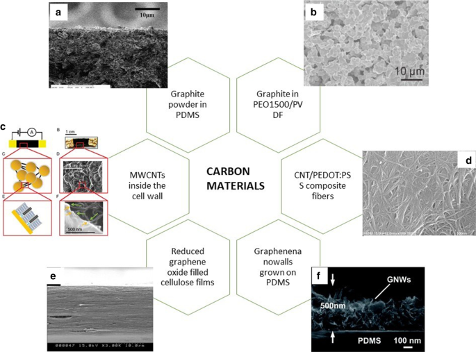
各种基于碳材料的柔性温度传感器。 一 石墨-PDMS 复合材料的 SEM 图像 [67]。 b PEO1500/PVDF/Gr 的整个表面显微照片 [68]。 c Cyberwood 的示意图和扫描电子显微镜 (SEM) 图像 [76]。 d CNT/PEDOT:PSS 复合纤维的 SEM 图像,CNT 含量为 40 wt% [75]。 e CrGO100 的 SEM 图像 [54]。 f GNWs在PDMS上的横截面SEM图像[86]
制造生物材料的常规方法依赖于生物结构、仿生学和生物灵感的逆向工程。生物结构通常优于人造材料。例如,高等植物以高响应性感知温度变化。如图 2c 所示,Giacomo 等人。 [76]利用植物纳米仿生技术提出了一种由分离的植物细胞和碳纳米管(MWCNT)制成的具有优异温度响应敏感性的仿生材料。使用碳纳米管作为通道直接连接细胞,创造了一种仿生材料,其有效温度电阻率 (TCR) 为 \(- \,1730\% \,{\text{K}}^{ - 1}\),即比目前最好的传感器高两个数量级,监测温度范围为 35-75°C。许多类型的温度传感器研究可以在较窄的温度范围内实现高灵敏度,但在较宽的温度范围内(40 K),响应性能不足。还要参考自然界中蛇的生物温度传感结构——蛇的坑膜,生物膜具有异常高的温度和距离敏感性。它可以用来定位一定距离的温血猎物。他们使用了 Ca 2+ 将离子注入果胶膜以模拟蛇脸颊膜的传感机制,以制备添加有 CaCl2 的果胶水凝胶温度敏感材料 [10]。可以以 <10 mK的灵敏度映射和监控温度源,并在一定距离内感知温暖的物体。结合植物细胞或模仿动物生物结构提供了新的思路,使柔性传感器的研究方向更加广泛。
石墨烯是一种二维混合碳层,具有六边形蜂窝晶格 [77, 78]。有大量离域电子,使其独特的电荷传输允许高载流子浓度(\({10}^{{{33}}} \,{\text{cm}}^{ - 2}\)),在某些环境条件下,迁移率超过\({10}^{5} \,{\text{cm}}^{2} \,{\text{V}}^{{ - {1}}} \, {\text{s}}^{ - 1}\)。并且空间结构可以提供丰富的位点。修饰官能团以满足各种应用要求。同时,它具有高流动性、优良的导热性、优良的透明性、高达\(1\,{\text{TPa}}\)弹性模量的机械性能、化学稳定性和生物相容性[79]。它在各种电子设备的应用领域引起了广泛关注[80]。具有优异电子和机械性能的透明氧化石墨烯(GO)或还原氧化石墨烯(rGO)是石墨粉经过氧化或进一步还原后形成的具有层状结构的产物[81, 82]。表面含有羟基、羧基和环。许多官能团,例如氧基,很容易被修饰,并且对环境条件(包括湿度、温度和化学物质)以及可见响应特性敏感 [54, 83]。然而,氧化石墨烯 (GO) 的低电导率不适用于电子设备。还原氧化石墨烯 (rGO) 通过热还原合成以提高导电性。柔性温度传感器也需要其出色的温度灵敏度 [54, 84, 85]。通过采用等离子体增强化学气相沉积 (PECVD) 技术 [77] 和聚合物辅助转移方法,石墨烯纳米壁 (GNW) 生长成垂直于基板的石墨烯纳米片。生长过程形成交错结构,使其具有更高的应变性能[61, 83]。优异的机械性能也已应用于研究中的温度传感器。多用途石墨烯及其衍生物在电子皮肤应用中的应用,为制备性能优良、透明、功能丰富、制造工艺简单的柔性温度传感器铺平了道路。
严等人。 [58] 制造了一种柔性温度传感器,该传感器使用三维褶皱石墨烯作为活性材料,可以通过光刻过滤方法监测 30-100°C 范围内的温度 [34]。由于类弹簧结构的特殊性,温度变化传感特性可以在高达 50% 的应变下表征。传感器在无应变条件下的 TCR (\(- \,1.05 \pm 0.28\% \,{\text{K}}^{ - 1}\)) 高于报道的硅纳米线温度传感器 (\(0.15 - 0.37\% \,{\text{K}}^{ - 1}\)) 次。值得注意的是,这种结构的散热材料的热指数是可以调整的。温度响应和恢复可在几十秒内完成,与传统的刚性陶瓷热敏电阻相比,增加了其适用性。刘等人。 [87] 使用 rGO 材料作为温度敏感材料,通过印刷技术制造了一种轻便、低成本、灵活的温度传感器。监测温度为20-110°C,灵敏度为\(0.6345\% \,^{ \circ } {\text{C}}^{ - 1}\),响应时间可达1.2 s。具有特定的应力应变特性,可附着于特定的曲率表面。在相同的实验条件下,通过比较还原氧化石墨烯(rGO)、单壁碳纳米管(SWCNTs)和多壁碳纳米管(MWCNTs)的线性度、灵敏度、机械性能和重复性,发现表明以rGO为活性材料的温度传感器的性能最为均衡,为今后大规模制备电子皮肤提供了思路。萨达西夫尼等人。 [54] 提出了一种使用纤维素作为基质和热 rGO 作为填料的复合薄膜,以根据温度变化产生 25-80°C 的灵活有效的监测温度范围。(如图 2e 所示)电容式柔性温度传感器呈线性关系。与标准的商用铂金温度传感器相比,该温度传感器不会因金属腐蚀现象随时间推移而造成污染,可长期保持稳定。 Trung 等人。 [17]通过简单的旋涂方法和层压技术制造了透明和可拉伸(TS)柔性温度传感器。由 rGO 纳米片和弹性聚氨酯 (PU) 基材形成的温度传感层。复合材料的形成。该电子器件的新颖之处在于结构中的每一层材料都是TS,可以很容易地直接涂覆在透明且可拉伸的基板上。然后它可以很容易地附着在人体上。该设备可以检测小至 0.2°C 的温度变化。在以 30% 的应变拉伸 10,000 次后,它对温度响应几乎没有影响。该装置在应变为 70% 时仍可使用。杨等人。 [86] 提出使用等离子体增强化学气相沉积 (PECVD) 技术在铜箔上生长特殊的交错 3D 导电 GNWs 网络结构(图 2f),结合聚合物辅助转移方法和 PDMS 形成超灵敏可穿戴温度传感器。热响应远远超过传统温度传感器。 GNW 出色的延展性和热灵敏度与 PDMS 的大膨胀系数相结合,使传感器能够以 0.1°C 的精度监测 25-120°C 的温度变化,响应时间为 1.6 秒,恢复时间为 8.52 秒,并在几个月内保持稳定。 TCR 达到 \(0.214\,^{ \circ } {\text{C}}^{ - 1}\),比标准商用铂金温度传感器高两个数量级 (\(39.2 \times 10^{ - 4 } \,^{ \circ } {\text{C}}^{ - 1}\))。碳材料在柔性温度传感器中的应用促进了其在健康监测、可穿戴设备、机器人、人机界面和人造皮肤等方面的应用潜力。
金属和金属氧化物
金属材料一般为金(Au)[88,89,90]、银(Ag)[91、92]、铜(Cu)[93]、铂(Pt)[55、94]等导电材料(在图 3c)、镍 (Ni) [95] 和铝 (Al) [96],主要用作传感器的电极和导线。与传统的刚性金属温度传感器相比,柔性金属温度传感器具有较高的机械柔韧性,可以很容易地附着在高度弯曲的表面上,更适合检测小范围内发生的微小温度变化和分布。就目前的印刷工艺而言,一些金属材料对温度敏感且具有良好的导电性,由导电金属纳米油墨[97]、纳米填料[95]、纳米线[98]、图案化薄膜制成活性温度敏感层[19],广泛应用于柔性温度传感器。
<图片>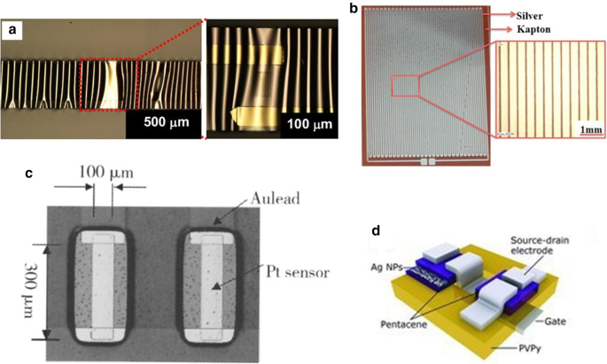
各种基于金属材料的柔性温度传感器。 一 PDMS 基板顶部的可拉伸传感器,具有周期性弯曲图案 [99]。 b 在 Kapton 基板上喷墨印刷的银温度传感器的照片 [102]。 c 温度传感器的图像 [6]。 d (一个晶体管)-(一个热敏电阻)温度传感器原理图[101]
典型温度传感器中最常见的敏感材料是 Pt 和 Au。斌等人。 [6] 使用微机电系统 (MEMS) 技术并提出铂作为传感材料,在剥离过程后沉积在 PI 膜上。层压形成所需图案后,用于监测20-120℃的温度变化,TCR值为\(0.0032\,^{\circ} {\text{C}}^{ - 1}\ )。与昂贵的铂金相比,金具有更好的导电性和柔韧性。为了实现器件的性能不受拉伸应变的影响,Yu 等人。 [99] 在预拉伸的 PDMS 柔性基板 Chromium(Cr)/Au 薄膜(图 3a)上巧妙地使用溅射沉积,并通过光刻工艺制造了一个可逆的可弯曲和可拉伸的柔性温度传感器。当设备的最大拉伸为 30% 时,设备的性能不会改变。研究改善了柔性传感器抗拉性差的缺陷。丹科科等人。 [100] 使用有机银复合油墨通过喷墨印刷在聚酰亚胺薄膜上平滑均匀地沉积银线(见图 3b)。它使可测量的体表温度为 20-60°C,可以弯曲且灵活的温度传感器。平均灵敏度为 \(2.23 \times 10^{3} \,^{ \circ } {\text{C}}^{ - 1}\)。但是,传感器具有 <5% 的滞后。任等人。 [101] 基于银纳米粒子 (NPs)/并五苯热敏电阻和有机薄膜晶体管 (OTFT) 的集成,提出了一种具有高热分辨率(动态范围 =10 位)的柔性温度传感器,温度范围为 15-70° C。该研究测试了复合材料对温度的高度依赖性,并证明了银纳米粒子 (NP) 在热敏电阻应用中的可行性。高动态范围传感器也适用于大面积传感器阵列和电子皮肤。全等人。 [95] 开发了一种柔性温度传感器,设计有半结晶聚乙烯 (PE) 和聚氧化乙烯 (PEO) 聚合物的混合物,其中填充有镍颗粒。其中,当镍颗粒的浓度超过镍填料的渗透阈值时,高电导率(\(40 \,{\text{S}}\,{\text{cm}}^{ - 1}\))可以得到。由于二元聚合物混合物特有的大正温度系数(PTC),所制造的传感器不仅可以提供可调节的敏感温度范围,同时保持热循环的稳定性,以实现可重复的温度响应过程。该传感器的灵敏度比标准热电偶和无线传输高三个数量级(\(0.3\, {\text{V}}\,^{ \circ } {\text{C}}^{ - 1}\))函数,但存在 ± 3.1°C的显着误差。值得注意的是,他们希望将无线传感技术与可印刷材料相结合,以实现广泛的应用。
金属氧化物也是重要的活性材料,广泛应用于温度传感器。金属氧化物材料的高电阻温度系数可以提高感温性能。金属氧化物半导体的热敏性是半导体化合物在不同温度下发生变化,电阻值发生变化的现象。廖等人。 [103] 报道了一种含有无机热材料二氧化钒(VO2)的高灵敏度温度/机械双参数传感器,该传感器基于通过转移印刷技术(VO2)/PDMS 多层结构制造的PET/二氧化钒。通过聚合物辅助沉积 (PAD) 技术沉积的 VO2 层被蚀刻并附着在 PDMS 薄膜上。它可以检测 270-320 K 范围内的温度。 分辨率为 0.1 K 的温度传感性能归功于 VO2 材料的高 TCR。为了准确绘制体表温度变化,Huang 等人。 [91] 开发了一种喷墨打印工艺。使用氧化镍 (NiO) 在 PI 膜上生成稳定的纳米粒子墨水。微小的方形 NiO 薄膜印在银导电轨道之间的末端,以快速制造温度传感器。它在弯曲测试下仍能保持性能,并具有与热电偶相似的响应速度。对金属和金属氧化物的广泛研究,为金属材料在基于金属材料热特性的柔性温度传感器领域的应用奠定了基础,并进行了有趣的探索。
聚合物和有机材料
聚合物是柔性传感器中最常用的材料。除了用作基材或活性剂外,热敏复合材料具有机械柔韧性、重量轻、透明、性能稳定、易加工、制造成本低等特点。在温度传感器中的应用备受关注。温度传感器中常用的热敏聚合物包括聚(3,4-乙烯二氧噻吩)-聚(苯乙烯磺酸盐)(PEDOT:PSS)[16, 104,105,106]、聚(3-己基噻吩)(P3HT)[107]、聚吡咯( PPy)[57]、并五苯[101]、聚(N-异丙基丙烯酰胺)(pNIPAM)[108]、聚偏二氟乙烯(PVDF)[109,110,111,112,113]等
Based on a circuit design strategy [114] that can improve the accuracy and robustness of a stretchable carbon nanotube temperature sensor, Zhu et al. [115] used differential readout technology to compare the composition of the active, sensitive layer of a stretchable temperature sensor based on OTFTs (see Fig. 4a). Among them, Polystyrene- block-poly(ethylene-ran-butylene)-block-polystyrene (SEBS) with azide-crosslinke and Poly(diketopyrrolopyrrole-[3,2-b]thieno[2′,3′:4,5]thieno[2,3-d]thiophene]) (PDPPFT4) and Poly(isoindigo-bithiophene) (PII2T) these two organic semiconductors (OSCs) are blended and spin-coated on the gate dielectric, CNTs are used as electrodes, and the temperature measurement range is 25–55 °C. Inside, the temperature coefficients of the two sensors are \(- \,2.89\% \,^{ \circ } {\text{C}}^{ - 1}\) and \(- \,4.23\% \,^{ \circ } {\text{C}}^{ - 1}\), respectively. When the uniaxial strain range is 0–30%, the errors are < 1 °C and < 1.5 °C, respectively, further show the feasibility and generalizability of differential readout method and OSCs in stretchable sensors are discussed.横田等人。 [116] reported a large-area super-flexible temperature sensor based on a semi-crystalline acrylate polymer/graphite composite material that can be measured at multiple points and can be printed (in Fig. 4b). Between 25 °C and 50 °C, it shows noticeable resistance changes at this temperature, which is suitable for measuring the physiological temperature changes of the human body. It has stable thermal cycle stability, the sensitivity of up to 20 mK, and a high-speed response time of less than 100 ms. In in vivo experiments, the stable changes in the rat's lungs' core temperature measured, but the high resolution of the sensor proved to be 0.1 °C. The sensor array based on the above characteristics realizes the dynamic visual, thermal imaging demonstration of the spatial temperature change. However, the air permeability of the equipment components is not right, and the long-term wear is one of the problems to be solved.

Various flexible temperature sensors based on thermosensitive polymer. 一 A sample with two temperature sensors on a fingernail [115]. b Photograph of a film of copolymer with graphite filler (scale bar, 1 cm) [116]. c Photograph of a Te-nanowire/P3HT-polymer composite device on a flexible Kapton substrate [107]. d Photos of the DN hydrogels self-healing process [121]. e Photographic image of the fabricated temperature sensor attached onto palm skin and the overall schematic illustration of the octopus-mimicking microstructured adhesive [108]
Self-supplied energy has always been the focus of many people's attention [117]. The realization of self-supplied energy by flexible equipment will significantly reduce the equipment's need for external energy, making flexible equipment more portable and more straightforward [118]. Among them, the thermoelectric polymer materials are the realization of self-supplied energy required.杨等人。 [107]developed a flexible thermoelectric nanogenerator (TENG) based on a clean composite thermoelectric material formed by Te-nanowires grown at room temperature and poly(3-hexyl thiophene) (P3HT) polymer (shown in Fig. 4c). TENG can generate electricity only with a temperature difference of 55 K. Because of the characteristics of thermoelectric materials, TENG can be used as a flexible temperature sensor to monitor the temperature difference of the entire device, and use human body temperature as an energy source to directly power the sensor. The monitoring sensitivity at room temperature is 0.15 K. Besides, they also demonstrated another self-powered temperature sensor with a response time of 0.9 s and a minimum temperature change of 0.4 K at room temperature. The small temperature resolution makes the sensor device can monitor the temperature change of the fingertip. Self-supplied can make flexible sensor equipment more independent and reduce weight. It is also a possibility for the development of flexible sensors in the future (Table 2).
Low-cost, environmentally friendly, easy-to-obtain, and process materials with excellent biocompatibility have always been an essential condition for human beings to pursue to meet mass production continuously [119]. There is such an almost inexhaustible biological material–cellulose, which has excellent properties. Its elasticity and other advantages also play an essential role in flexible sensor devices and can be used as a flexible substrate. Polypyrrole (PPy) is a linear biocompatible polymer with excellent electrochemical stability and rapid response. Mahadeva et al. [57] reported a method based on in-situ polymerization-induced adsorption that combines unique cellulose and nano-thickness polypyrrole (PPy) excellent electrical properties to form a temperature and humidity sensitive composite. The material used to fabricate an environmentally friendly, low-cost, bio-adaptable flexible temperature sensor. Because of the sensitivity of materials to humidity, as the temperature increases, the sensor's capacitance also increases. Hydrogels have received continuous attention in recent years of research [120, 121]. Because of its good self-healing ability, excellent toughness and stretchability, and biological adaptability, it has aroused great research interest in application fields such as flexible electronics, health monitoring, and biomedical diagnosis [122, 123]. However, ionic hydrogel, as a good ion conductor, can respond to a variety of stimuli, hydrogels with weak mechanical strength, and reduced temperature sensitivity present challenges in applying flexible temperature sensors. To solve the disadvantages of traditional hydrogels, An et al. [121] proposed a double-mesh ion-conducting double-network (DN) hydrogel with excellent temperature sensors' self-healing properties. The DN hydrogels self-healing process is shown in Fig. 4d. The addition of carbon nanotubes with high thermal conductivity to the hydrogel with dynamic physical crosslinking and high conductivity hydrophobic association network and ion association network improves the temperature sensitivity of DN hydrogel. The linear hydrogel temperature sensor can perfectly fit the surface of complex objects and produce sensitive resistance changes. The research and development of this material expand hydrogels' application in the fields of biomedicine and flexible electronics.
In recent research, PEDOT:PSS is a new type of organic conductive polymer that often used in printable, flexible temperature sensors [124]. Generally speaking, PEDOT:PSS has the advantages of high conductivity (\(10^{3} \,{\text{S}}\,{\text{cm}}^{ - 1}\)), excellent thermoelectric performance [125,126,127,128], strong stability [123, 129], and transparency when doped [60]. Most polymers are p-type semiconductors. By adding some solvents, such as dimethyl sulfoxide(DMSO) [130] or polyhydroxy organic compounds, such as ethylene glycol [131], the conductivity rate of the polymer can be increased dozens of times or even hundreds of times. Harada and colleagues used different composite ratios of CNTs and conductive PEDOT:PSS solutions to produce a series of composite heat-sensitive films with temperature sensitivity within \(0.25 - 0.78\% \,^{ \circ } {\text{C}}^{ - 1}\) through various printing processes [11, 132,133,134]. The sensing performance is better than the typical metal temperature sensor. Some of the devices exhibited a near body temperature resolution of less than 0.1 °C or fast response time of 90 ms. The research team used various printing methods to create a variety of flexible temperature sensors with different structures and outstanding performance, in addition to enriching the flexible temperature sensors applications in medical and health, wearable devices. Have also triggered everyone thinking about printable, flexible sensors. The fabricating details of printable, flexible temperature sensors will be expanded in the next unit. In addition to changing the composite ratio will affect the performance of the composite film, the structural improvement will also optimize the properties of the same composite film. As Fig. 4e shown, Oh et al. [108]demonstrated a biological material made by a photolithographic stripping process and a spin coating process, inspiringly imitating the adhesion structure of octopus foot sucker. It is a high-sensitivity resistor temperature sensor composed of poly(n-isopropyl acrylamide) (pNIPAM) temperature-sensitive hydrogel, PEDOT:PSS and CNTs. The device has a sensitivity of \(2.6\% \,^{ \circ } {\text{C}}^{ - 1}\) in the temperature range of 25–40 °C, and can accurately detect skin temperature changes of 0.5 °C. Because of the microstructure similar to the suction cup and its viscosity, the device has a certain degree of resistance to bending, non-irritating, long-lasting, and reusable binding effect.
Transparent and scalable nanocomposite field-effect transistor based on polyvinylidene fluoride (PVDF) and its copolymer polyvinylidene fluoride (P (VDF-TrFE)) with high stability, strong mechanical properties, and low distortion, it is often used in pressure sensing, strain sensing, and infrared (IR) light-sensing devices [135, 136]. Interestingly, researchers have found that this type of device is also highly responsive to infrared radiation from the human body, so it is predicted to be used to monitor the human body's physiological temperature changes [137]. Trung and colleagues, based on previous research experience [113, 138], use rGO/(P(VDF-TrFE)) composite sensing active layer as the channel through a simple spin coating process, integrated PEDOT:PSS can fabricate adjustable flexible field-effect transistor (FET) temperature sensor [139]. The film's temperature response and transparency can adjust by changing the concentration of rGO and the thickness of the composite film (Fig. 5a). The sensor can monitor temperature changes from 30 to 80 °C. With 0.1 °C resolution and monitoring ability, and super high-temperature response, excellent temperature sensing performance verifies the feasibility of the application of pyroelectric polymer materials in the field of softcore temperature sensors. Similarly, Tien et al. [112] in order to realize that the sensor can collect pressure and temperature signals without mutual interference, they proposed the use of field-effect transistor (FET) sensing platform to change the material of the response sensitive layer, based on their previous the research concluded that a mixture of polyvinylidene fluoride (P(VDF-TrFE)) and BaTiO3(BT) nanoparticles (NPs) is used as piezoelectric (see Fig. 5b), pyroelectric gate dielectric and pentacene are used as organic semiconductor channel for pressure thermal resistance directly integrated into the FET platform when the flexible sensor is under multiple stimuli, it decouples the output signal and minimizes the signal interference of strain coupling. The FET sensor can disproportionately present strain and temperature at the same time. The FET sensor array can also visually respond to stimuli, exhibiting the advantages of low energy consumption and low failure, which shows a possibility for the application of large-area multi-modal flexible sensors in the field of electronic skin in the future. Flexible multi-parameter OFET devices that can be printed and fabricated in a large area have excellent application potential in biomedical monitoring, infrared imaging, and electronic skin.

Flexible temperature sensor containing PVDF material. 一 Schematic of transparent, flexible rGO/P(VDF-TrFE) nanocomposite FET. The schematic illustrates structural, optical (transparent) and electrical (response to temperature) properties of the transparent, flexible R-GO/P(VDF-TrFE) nanocomposite FET [113]. b The structure of physically responsive field-effect transistor (physi-FET) with the bottom-gated and top-contact structure, where the gate dielectric is comprised of nanocomposite of P(VDF-TrFE) and BaTiO3 nanoparticles and the channel is organic semiconductor of pentacene [112]. c Schematic diagram of the ZnO/PVDF composite film and rGO electrodes [110]. d Photograph of the flexible MFSOTE matrixes [23]
In addition to the decoupling method to reduce or eliminate signal interference, in order to solve the problem of mutual interference of multi-parameter flexible sensor signals, Lee et al. [110] proposed a method of inferring temperature based on the recovery time of the resistance change signal, so that the semiconductor zinc oxide (ZnO) nanostructure is mixed into the substrate polyvinylidene fluoride (PVDF) as a filler (As shown in Fig. 5c) to make a highly sensitive multifunctional sensitive layer that can collect temperature and pressure signals at the same time. Among them, the semiconductor ZnO can increase the dielectric constant of PVDF, and it also has thermal stability.张等人。 [23] reported a dual-parameter flexible sensor based on a self-powered microstructure-frame-supported organic thermoelectric (MFSOTE) material. The Fig. 5e show the flexible MFSOTE matrixes. By converting the signal changes caused by temperature and pressure stimulation into two independent electrical signals, the temperature and pressure simultaneously sensed. This unique material shows excellent temperature sensing characteristics. The monitoring temperature range is 25–75 °C, The resolution can achieve < 0.1 K, the response time under 1 K temperature difference is < 2 s, and it can also be adjusted according to different substrates to meet the sensing needs.
Fabrication
With the increasing requirements for flexibility, multi-function, simple fabricating, and high sensitivity of electronic devices, the exploration and discovery of flexible sensor fabricating methods with a lightweight, simple process, low cost, and large-area fabricating have always been what researchers are keen [140]. This section mainly summarizes the recently reported and feasible fabricating strategies of flexible temperature sensing elements and discusses the key processes to improve their performance.
Thin Film Deposition
The thin film preparation method can be divided into vapor deposition and phase deposition according to the phase of the material used. The phase deposition includes spin-coating and inkjet printing processes mentioned later. In contrast, the vapor deposition depends on whether the deposition process contains the chemical reaction process divided into physical vapor deposition (PVD) and chemical vapor deposition (CVD).
PVD is to depositions or atoms generated by physical methods on a substrate under vacuum conditions to form a thin film, which generally used to prepare electrodes or active metal layers [141, 142]. Common deposition methods include vacuum evaporation, vacuum sputtering, and ion plating. Among them, the metal target ion sputtering refers to the vacuum container, under the action of high voltage 1500 V, the remaining gas molecules are ionized to form plasma, and the cations bombard the metal target under the acceleration of the electric field, causing the metal atoms to sputter on the surface of the sample to form conductive film [143]. Ahmed et al. [144] introduced a Si-temperature sensor based on a flexible PI substrate. They deposited undoped amorphous silicon as a sensing material between metal electrodes formed by radio frequency magnetron sputtering and packaged them. Finally, the temperature sensing element is embedded in the flexible polyimide film, and the sensing performance is not affected. The maximum TCR at 30 °C is \(0.0288\,{\text{K}}^{ - 1}\).韦伯等人。 [145] introduced two ultra-thin, skin-like sensor fabricating methods that are self-assembled on the skin surface in the form of an array to provide clear and accurate thermal performance monitoring. A structure is composed of a temperature sensor array, the sensitive layer formed by the serpentine trace structure of the Cr/Au layer deposited on the PI film by the metal evaporation deposition method, the microlithography technology, and the wet etching technology, and the reactive ion etching and metal deposition for contacts and interconnections complete the array. Another sensor structure uses multiplexed addressing to form a patterned PIN diode sensor design of doped Si nano-film. The sensitivity layer is defined by metal evaporation, photolithography, chemical vapor deposition, and wet etching steps. The two arrays are shown in Fig. 6a. Aluminum phthalocyanine chloride (AlPcCl) is often used as a material for solar cells and humidity sensors. Under the study development of Chani et al. [146] AlPcCl is used as a thermistor and deposited on an aluminum electrode on a glass substrate using a vacuum thermal evaporator. The authors found that the AlPcCl film has a higher sensitivity to the temperature at 25–80 °C, and annealing can improve sensing performance. In a flexible temperature sensor developed by Bin et al. [6] that uses Pt resistors as the thermosensitive material, Pt is evaporated on the Al layer deposited on the spin-coated PI film, and the Pt layer is patterned as a sensitive the layer is spin-coated and packaged with polyimide material. After hydrochloric acid treatment, a complete flexible temperature sensor is peeled off, which can be used to measure the surface temperature of objects in the biomedical field.

Fabrication method of flexible temperature sensor method of flexible temperature sensor. 一 Top:Optical images of a 4 × 4 TCR sensor array integrated on a thin elastomeric substrate with magnified views of a single sensor. Bottom:Optical images of a 8 × 8 Si nanomembrane diode sensor array integrated on a thin elastomeric substrate with magnified views of a single sensor [145]. b Schematic process for the fabrication of GNWs/PDMS temperature sensors [86]. c Sketch of the implantable micro temperature sensor on polymer capillary and its application. The head spiral sensing element is fabricated by photolithography [157]. d Schematic for each layer of the e-skin device [132]. e Schematic of the e-skin fabrication process on a PET substrate using a printing method [134]
Compared with other thin-film preparation processes, the chemical vapor deposition method can achieve high-purity and high-quality thin films. It can be structured and controlled at the atomic layer or nanometer level [147,148,149]. The process of synthesizing GNWs film on copper foil by low-pressure radio frequency plasma enhanced chemical vapor deposition (RF-PECVD) technology.杨等人。 [86] developed a flexible temperature sensor based on GNWs/PDMS. The fabricating process is shown in Fig. 6b. They verified GNWs is feasible as an active layer of a temperature sensor, and its thermal response performance exceeds that of a traditional metal temperature sensor. Compared with traditional CVD technology, using PECVD technology [150] under low temperature and low-pressure conditions can effectively improve the deposition rate and film quality. In another study, Zhou et al. used the floating catalyst chemical vapor deposition (FCCVD) method [151] to synthesize the original SWCNT film with a controllable thickness directly. The continuous network of CNTs grown by this method has significant conductivity and a high favorable Seebeck coefficient. After transferring the original SWCNT film to the PET substrate, drop-cast the branched polyetherimide (PEI) ethanol solution, and dry it to obtain an n-type SWCNT film that can be used in the fabricate of flexible thermoelectric modules. Although CVD can achieve the deposition of any material on any substrate, as the demand for simple, low-cost and large-area fabricating nanodevice fabricating technology continues to grow, the fabricating process is complex, high-cost, and toxic CVD growth processes and The time-consuming etching process is being replaced by more suitable flexible electronic device fabricating technology [58].
Micro-nano Patterned Fabrication
Thin-film patterning is one of the core technologies of flexible electronics fabricating. It follows the basic idea of removing materials from top to bottom or adding materials from bottom to top in the fabricating industry. Its key technologies are thin-film fabricating, patterning, transfer, replication, fidelity, and other crafts. Flexible electronics require large-area, low-temperature, low-cost patterning technology. Learned from the patterning technology of microelectronics and micro-electromechanical devices. However, at the same time, we must consider the characteristics of flexible electronic devices such as flexible substrates, organic materials, and large areas. The patterning technologies currently available for flexible temperature sensors include lithography, printing, soft etching, nanoimprinting, inkjet printing, laser sintering, transfer printing, nano-direct writing [152], and other processes.
Lithography is a patterning method to realize various and ingenious geometric figures or structures in flexible electronics. The photolithography process involves transferring the pattern on the photomask to the substrate by using the photoresist with different sensitivity and physical and chemical reactions under the light. The photolithography process usually uses photoresist on an insulator (usually a silicon wafer) to pattern the required pattern or structure after spin coating, and further realize it through a stripping process [153, 154]. Because of the photolithography process and the stripping process, high alignment and etching accuracy, simple mask production, and comfortable process conditions can usually achieve high-precision, feature-rich microstructure systems. In the ultra-thin flexible suture application with an integrated temperature sensor and thermal actuator developed by Kim et al. [155], they used photolithography technology to micro-process the equipment, and the fabricated flexible medical equipment has the stable thermal performance. Lithography technology limited by the necessity of available materials and precision equipment. The thickness of processable materials and thin films are limited. It is not suitable for device fabricating processes that require a large number of active materials.杨等人。 [156] proposed a flexible implantable micro temperature sensor, and used surface microlithography to etch the micro flexible temperature sensor on the outer surface of the polymer capillary (The sensing principle diagram of the miniature thermometer is shown in Fig. 6c). Using Pt as a sensitive material has good linearity, and it has a promising future as an implantable temperature sensor in the biomedical field. However, this technology is the foundation of the microelectronics industry and pioneered the era of wearables flexible electronics.
With the development of science and technology, the printing process has expanded from the traditional text and image field to the micro-nano structure patterning field. technology can deposit various materials on various substrates, and the printing process is not harsh on the environment. In a nutshell, printing technology includes letterpress, lithography, gravure, screen printing, and has evolved into soft etching [158, 159], transfer printing, nanoimprinting, and other methods. According to the specific implementation method, the wearable sensor can distinguish the printed part from the non-printed part with the mask help. In mask printing, the pattern to be transferred must be designed in advance and then formed through the mask. The functional, active material can directly be transferred to the substrate or electrode through the functional ink imprinting process [160]. Screen printing is a typical mask printing technique [161]. In the printing process by absolute pressure, the functional ink is transferred to the substrate through a squeegee with a patterned mesh to form a pattern. The unique printing method allows screen printing to achieve fast, large-area low-cost fabricating requirements on flat or curved surfaces. It has been widely used in fabricating sensor working circuits, electrodes, and sensor sensing elements. Compared with photolithography technology, screen printing can produce patterns on various materials. However, its pattern resolution cannot meet complex geometric shapes requirements and is only suitable for making patterns with simple shapes.横田等人。 [116] stirred and mixed a variety of semi-crystalline polymers with graphite to form a super-flexible temperature-sensitive copolymer for flexible temperature sensors for human physiological temperature monitoring. The super-flexible temperature sensor element is printed by mask printing by sandwiching the copolymer mixed with graphite filler between two interdigital gold electrodes deposited on the PI film and then forming by hot pressing.严等人。 [58] used a flat-plate suction filter printing method to deposit graphene through a mask, vacuum filter it, and transfer it to the substrate to form a three-dimensional fold pattern structure produce stretchable graphene with a variable thermal index. The thermistor increases the sensing area and stretchability of the sensor. The pre-designed stretchable sensitive material pattern can still maintain sensitive monitoring of temperature when stretched to less than 50%. To achieve the economical fabricating of sensors with a larger area, Harada and colleagues abandoned complex and costly fabricating processes (such as deposition and photolithography). They chose to fabricate a series of multifunctional flexible sensors using only printing processes. The PEDOT:PSS/CNT composite ink printed on the circuit formed by screen printing on the PET substrate through a shadow mask, and there are holes after laser writing (LS) to combine with the lower layer of PDMS. The fingerprint-like structure (see in Fig. 6d) is combined with the screen-printed strain sensor layer to form a flexible sensor array. The deformation and temperature difference caused by the contact contacts achieve a human-like monitoring performance. In another study, also using full printing technology, Kanao et al. [134] proposed a multifunctional flexible sensor array based on a cantilever beam structure (Fig. 6e). They placed strain sensors and temperature sensors on a flexible screen-printed circuit. On both sides of the PET substrate, a patterned shadow mask with a flexible temperature sensor (PEDOT:PSS/CNT composite ink) printed on the screen's electrical contacts printed circuit. The fully printed array sensor used to imitate the sensing characteristics of human skin. When the cantilever beam structure strained, the heat source is closer to the temperature sensor on the substrate's bottom surface to monitor temperature changes more accurately.
Transfer printing is a printing method that the patterned surface concave structure or convex structure transferred to the receptor substrate through a non-patterned stamp. The basic principle is to use the different viscosity of the printing layer relative to the stamp and the substrate to achieve pattern transfer [162,163,164,165]. There are two types of transfer printing:direct transfer printing and indirect transfer printing. In the fabricate of flexible temperature sensors, the latter often used, that is, the use of a pre-printed patterned film to transfer to the receptor substrate. In the previous review, many examples of organic materials are sensitive layers mentioned, but few inorganic materials are used as temperature-sensitive materials. It is worth noting that Liao et al. [103] reported a high-sensitivity temperature/mechanical dual-parameter sensor containing inorganic thermal material vanadium dioxide (VO2), which based on PET/vanadium dioxide fabricated by transfer printing technology (VO2)/PDMS multilayer structure. The VO2 layer deposited by polymer-assisted deposition (PAD) technology is etched and attached to the PDMS film. After stretching, nano-type spider web cracks formed, and then the layer press to the flexible PET substrate. It can detect the temperature in the range of 270–320 K. The temperature sensing performance with a resolution of 0.1 K attributed to the high TCR of the VO2 material. The collected temperature signal and the mechanical signal are separated through the algorithm's difference to achieve simultaneous monitoring the effect of temperature and mechanical changes. In order to solve the problem of the flexible temperature sensor's insufficient stretchability, Yu et al. [99], based on transfer printing technology, invented a flexible device that can maintain the sensor performance even when the flexible device is stretched or compressed by 30%. They used the Au/Cr layer as a thermistor to patterned on SOI through standard photolithography technology. The peeled heat-sensitive layer adhered through a flexible PDMS stamp, and then transferred and printed on a pre-stretched flexible PDMS substrate to release the substrate. The fabricating process of forming a stretchable flexible temperature sensor, as shown in the Fig. 7a.

Fabrication method of flexible temperature sensor. 一 Schematic illustration of the fabrication process [99]. b Fabrication of the stretchable and multimodal all-graphene E-skin sensor matrix [84]. c Process flow illustrating the fabrication of printed ferroelectric active matrix sensor arrays [169]. d Multifunctional e-whisker fabrication [11]
Inkjet printing is an accurate, fast, and reproducible thin-film fabricating technology, which has been widely used in sensor development. Compared with other printing methods, inkjet printing has the advantages of convenience, flexibility, rapidity, low cost, compatibility, accuracy, etc. [166,167,168]. The patterns of inkjet printing need to be post-processed (drying, curing, sintering, etc.) to be fully formed. Improve the performance of printed patterns by converting ink nanoparticles into continuous materials. The properties of the surface tension and viscosity of the ink during the printing process, the quality of the printed pattern also places high requirements on the performance of inkjet equipment [97]. Under the condition of a specific size of the substrate, the conductive track's length formed as long as possible, and the thickness, width, and spacing of the track are reasonable. Repeated experiments obtain the ejection coefficient of the inkjet system. For example, Dankoco et al. [102] used the ink printing method deposit a composite ink with silver as the main component on the PET film to make a flexible and bendable temperature sensor. The circuit on the substrate is clear and smooth, and the ink drops are consistent, which used to measure human body temperature. The picture shows the fabricating process of the extremely sensitive and transparent multifunctional electronic skin sensor matrix developed by Oh et al. [108] The flexible array has the function of monitoring temperature, humidity, and strain. It can feel sensations, such as breathing and touch. GO and rGO, which used as humidity and temperature sensing materials, are sprayed on the PDMS substrate of the graphene circuit grown by the CVD method through inkjet printing technology through a mask. The two sensors are horizontally and vertically aligned, and the temperature sensor is on the bottom layer (as shown in Fig. 7b). After cross-lamination, a PDMS/graphene pressure strain sensor is formed. As a multifunctional flexible sensor, it can collect at the same time but independently respond to a single signal. Inkjet-printed graphene is seven orders of magnitude higher than CVD-grown graphene. The performance advantages reflected in many articles, and some research results are better than CVD-made graphite products. Inkjet printing and screen printing are both rapid and low-cost technical means to realize large-area sensor fabricating. Zirkl et al. [169] combined the two rapid fabricating technologies to create a fully printed flexible sensor array that uses multiple screens. In printing and inkjet printing, only five functional inks used to easily integrate multiple functional electronic components (including pressure and temperature-sensitive sensors, electrochromic displays, and organic transistors) on the same flexible substrate (in Fig. 7c). Because the fabricating speed and low cost of the process can also be applied to the smart sensor network using the roll-to-roll (R2R) fabricating process in the future. The development of a disposable electronic skin system (EES) is particularly critical. Similar to the previous example. Vuorinen et al. [56] introduced a temperature sensor similar to a band-aid after inkjet printing. The sensor uses graphene/PEDOT:PSS composite ink and the printing done on PU material suitable for skin. In particular, in addition to being able to achieve a sensitivity higher than 0.06% \(^{ \circ } {\text{C}}^{ - 1}\), they used inkjet printers to perform serpentine patterned inkjet printing between the silver screen printed with a high resolution (1270 dpi) improved the lack of inkjet printing for printing complex graphics such as snakes. With the use and research of inkjet technology in flexible electronics, the technology for controlling nozzles and inks is also improving. Compared with the speedy fabricating process of screen printing, inkjet printing needs to go through a debugging process, and the printing speed is not as good as screen printing. Also, the small number of nozzles running simultaneously and the high nozzle failure rate limit the inkjet printing fabricating technology to laboratories, and the large-area fabricating requirements of industrial production cannot achieve.
Laser direct writing (LDW) technology uses calculations to design pre-designed patterns. It directly uses laser beam ablation without masking and vacuums deposition. It can directly complete pattern transfer on the surface of the substrate material, with good spatial selectivity and high direct writing speed and processing accuracy, short cycle, high material utilization, and low pollution. Compared with traditional temperature thermistors that require high temperature and a variety of complex processes to activate the sensing function, LDW can achieve selective annealing on a predetermined pattern. A novel integral laser induced by Shin et al. [170] The laser-induced reduction sintering (m-LRS) fabricating scheme can also reduce metal oxide NPs during the annealing process. Scratch NiO NPs ink on a fragile PET substrate, and use m-LRS technology to directly reduce NiO to pattern a linear Ni electrode to form a planar Ni–NiO–Ni heterostructure (as shown in Fig. 8a). The unique method of fabricating a complete flexible temperature sensor system composed of Ni electrodes and NiO sensing channels from a single material NiO NPs provides a new idea for the rapid fabricating of flexible temperature sensors. Different from the previously designed and fabricated fully-printed sensor arrays, Harada et al. [11] proposed a more direct method of mass-fabricating flexible temperature sensors based on previous research. The flexible temperature sensing composite ink printed on the substrate, using the laser for etching away the excess part directly, leaves the designed pattern on the substrate and completes the fabricate of the temperature sensor array. Cut the base to imitate the animal's whiskers to create an artificial electronic whisker (e-whisker) structure (Fig. 7d), strain sensor formed by laminated screen printing. Bionic sensor arrays can scan and perceive three-dimensional objects by using structural advantages.

Commonly used fabricating methods. 一 Schematic of the m-LRS process [170]. b Schematic diagrams showing fabrication process of the paper-based GNRs sensors [171]. c Fabrication process of the temperature sensors [87]. d Flexible temperature sensor on yarn, contacts made of polymer conductive paste [111]. e Fabrication process for the mold, adhesive, and temperature sensor [108]
Under the premise of realizing low-cost and large-area fabricating, disposable intelligent monitoring equipment not only allows monitoring behavior to use anytime and anywhere but also ensures the safety and hygiene of the flexible monitoring equipment.龚等人。 [171] proposed a pen-on-paper fabricating method that uses a brush write or a mask to graphene nanoribbon (GNR) conductive ink dripped between the carbon nanotube electrodes on the paper base. Shown in Fig. 8b. The flexible temperature sensor fabricated after encapsulation with transparent tape. In their research, GNRs have excellent sensing performance and meet the requirements for body temperature monitoring. The fabricating method provides reliable support for the application of fast, large-area disposable flexible equipment.
Other Commonly Used Fabricating Methods
Spin-coating the base layer, active layer, and encapsulation layer by layer is a common way to fabricate flexible temperature sensors by the liquid phase method. Spin coating technology often used for substrate fabricating and packaging protection. For solution-like sensitive materials, the spin coating used. The coating can not only significantly improve production efficiency but also has excellent potential for large-area fabricating.金等人。 [172] demonstrated the fabricating process of an organic field-effect transistor (OFET) array, using a spin-coating process to design a microstructure on a mold with a crystallized P(VDF-TrFE) material as a gate dielectric and other materials. Material packaging forms OFETs, and the introduction of microstructures enhances the sensing performance. The fabricating process of the bionic structure's [108] flexible temperature sensor fabricated. The adhesive layer of the bionic octopus foot sucker structure is fabricated by a spin coating process, combined with photolithography peeling technology and inverted mold technology (in Fig. 8e). It has an excellent temperature monitoring effect, and the materials used also perform well in terms of human biocompatibility.刘等人。 [87] After surface ionization treatment on the substrate, the flexible electrode was screen-printed, and then the sensitive layer rGO was connected to the flexible wire through the manufacturing method of air-spray coating, and the main structure of the temperature-sensitive flexible sensor was formed after packaging (see in Fig. 8c). It is possible to make robot skins.黄等人。 [68] fabricated a temperature sensor with flexibility, high resolution, and high repeatability in the temperature range of 25–42 °C. They dropped the PEO1500/PVDF/Gr composite solution after stirring and ultrasonic treatment on a polyimide flexible substrate. It was spin-coated at a certain speed to form a layer. It packaged it into a temperature sensor, which verified the medical body temperature transmission sense of possibility and feasibility. Spin-coating technology as an effective fabricating process for wearable devices has also introduced into Wu et al. research [173]. They designed an organic thin-film transistor with heat-sensing ability. Cleverly through the unique three-arm three-dimensional composite polylactide, polylactic acid (tascPLA) solution is spin-coated on the Au gate electrode evaporated on the Si substrate. Then the Au source and drain are deposited on it by a thermal evaporation method. The composite film containing tascPLA also serves as the gate of the OFET dielectric and substrate materials. In flexible electronics, there are not a few that use fabric as the carrier of the sensing element. The dip-coating of conductive yarn/fabric in conductive ink is the most commonly used coating technology for flexible sensors. The development of conductive fabrics provides a reasonable prerequisite for the application of smart fabrics. Sibinski et al. [111] developed a temperature sensor that monitors the temperature range of 30–45 °C. Moreover, it currently realizes filamentary miniaturization on a single yarn. In Fig. 8d shown, the PVDF monofilament fiber is coated with PMMA polymer compound mixed with multi-walled carbon nanotubes (MWCNTs) as a heat-sensitive layer by dip coating technology has good temperature sensitivity and extremely high repeatability. It is used as a fabric easily integrated into knit clothing. Another method, based on the molding properties of organic materials, is also used to fabricate flexible sensor membrane structures or to fabricate samples for testing sensing performance. The fabricating process of the thermoelectric nanogenerator (TENG) studied by Yang et al. [107] The drop-casting film method, after comparison, discards the PEDOT:PSS material, which has a weak drop-casting effect and is easy to break, not only the mixture of Te-nanowires and P3HT polymer in chlorobenzene solution is drop-casted on the flexible Kapton substrate to make a composite film, the composite material is also cast on the white fabric cloth, which also has apparent temperature sensing ability and thermoelectric performance, which can be used in wearable heat collectors. Rich and diverse fabricating methods lay the foundation for the development of flexible electronics. Under the requirements of large-scale and large-scale production, suitable fabricating technology is also continually developing. In the future, perfect wearable flexible devices are expected.
结果与讨论
Key Parameters of Flexible Temperature Sensor
The flexible temperature sensor can be attached to the human body to monitor the subtle temperature changes on the surface of the human body or real-time temperature monitoring of specific parts, and even the temperature of the core or tissues and organs in the body. They respond to temperature changes by changing the resistance and output the temperature changes as electrical signals. With the increasing demand for flexible electronic devices, the disadvantages of traditional temperature sensors, such as poor scalability, inability to carry, and poor real-time performance, are becoming increasingly unsuitable for flexible wearable devices. Today flexible temperature sensors are required to have high performance, such as high sensitivity, fast response time, reasonable test range, high precision, and high durability to realize the monitoring function better.
Sensitivity
Sensor sensitivity refers to the ratio of the change ∆y of the system response under static conditions to the corresponding input change ∆x , that is, the ratio of the dimensions of output and input. When the sensor output and input dimensions are the same, the sensitivity can be understood as the magnification [21, 174, 175]. The temperature coefficient of resistance TCR (TCR, in \(^{ \circ } {\text{C}}^{ - 1}\)) of the common resistance type flexible temperature sensor is expressed in the following expression, \(\Delta R/R_{0} =s\left( {T - T_{0} } \right)\), is the relative resistance change (\(\Delta R/R_{0}\)) as a function of temperature, where \(s\) represents TCR. If the sensor output and input show a linear relationship, the sensitivity is constant [83]. Otherwise, it will change with the input quantity. Generally speaking, by increasing the sensitivity, higher measurement accuracy can be obtained. Most flexible sensors used for body temperature monitoring only pay attention to temperature changes within 10 °C and therefore require high-temperature sensitivity to capture relatively small temperature changes. Here, several typical methods and concepts for improving the sensitivity of flexible temperature sensors are summarized to provide a favorable reference for further improvements.
The sensing performance of flexible temperature sensors is usually closely related to the properties of materials. One possible way to realize the development of sensitive sensors is to adopt composite materials with visible thermal performance. After temperature stimulation, the internal conductive network will change, which will lead to affect the temperature sensitivity of the device. To improve the temperature sensitivity of the active material, a strategy that converts temperature fluctuations into mechanical deformation is adapted to amplify the response of the conductive network to temperature changes. The thermosensitive material is connected to a substrate with a high positive thermal expansion coefficient to enhance thermal induction deformed. This method has applications in sensors made of graphene, graphite and graphene-nanowalls. For example, in the flexible temperature sensor designed and fabricated by Huang et al. [68], Gr establishes a conductive path in the PEO/PVDF binary composite material. In the process shown in the Fig. 9b. The temperature change will cause the PEO to transform from crystal to amorphous, and melt when the temperature is close to the melting point of PEO, the volume expansion of PEO will destroy the conductive network in the composite material, resulting in a sharp increase in resistivity-increasing the strength of the PTC, which can quickly reaction within a narrow temperature range change. Experiments show that PEO thermal performance plays a leading role in the PTC effect of the device. Another way to improve the sensitivity of a flexible temperature sensor is to use a unique structure. In recent years, to improve temperature sensing performance, various design strategies have been developed by changing the structure.余等人。 [176] recently proposed a method based on engineering microcrack morphology to change the crack morphology of the PEDOT:PSS film on the PDMS substrate by adjusting the substrate surface roughness, acid treatment time, and pre-stretching degree to improve the temperature sensitivity of the sensor. Figure 9d shows the effect of average crack length and cracks density on temperature sensitivity. The result is that the longer the crack length, the higher the crack density, and the higher the temperature sensitivity. It is proved that the micro-crack structure plays a vital role in the temperature sensitivity of the sensor. It is verified that obtaining a high-density micro-crack structure is the key to obtaining the high-temperature sensitivity of the sensor. High density and high length directly correspond to higher temperature sensitivity. The fabricating process of flexible electronic equipment plays a vital role in the production of the device and can effectively improve the sensitivity of the flexible temperature sensor. Just as Shin et al. [170] used a rapid overall laser-induced reduction sintering (m-LRS) method for fabricating Ni/NiO flexible temperature sensor is different from the inkjet printing method. They directly reduce and sinter the Ni electrode on the NiO layer, and form a high-quality overall contact between the metal electrode (Ni) and the temperature-sensitive material (NiO). Ni–NiO–Ni heterogeneous temperature sensor shows higher temperature sensitivity than other sensors of the same type (Fig. 9e). Raman spectroscopy and X-ray diffraction (XRD) measurements show that the superior sensitivity comes from the unique thermal activation mechanism of the m-LRS process. Besides, since flexible temperature sensors are mostly touch-sensitive, it is inferred that the film's thickness affects the sensitivity. The study of Lee et al. [177] verified the effect of the thickness of the highly sensitive paper base on the sensitivity, they use a simple dipping fabricating method to deposit sensitive materials on the printing paper. Dipping time will affect the thickness of the film. The Fig. 9f also shows the different performance of sensitivity due to different thicknesses. It should be noted that the higher the sensitivity, the narrower the measurement range and, worse, the stability. Therefore, it is necessary to pay attention to increasing stability and accuracy while improving sensitivity.

Sensitivity of flexible temperature sensor. 一 Images of the PEO1500/PVDF/Gr at room temperature. b Resistance curves of PEO1500/PVDF/Gr, PEO6000/PVDF/Gr and PEO5000K/PVDF/Gr composites versus temperature [68]. c The temperature measurement results before and after exercise, the illustration shows the flexible temperature sensor attached to the back of the hand. d Heatmap as functions of average crack length and crack density for TCR valuses from all developed sensors [176]. e PTC and NTC characteristics of the m-LRS processed Ni electrode and Ni–NiO–Ni structure. Inset digital images are m-LRS processed Ni electrode (upper) and Ni–NiO–Ni structure (lower) [170]. f The results of the deposited film thickness (blue circle), resistance at room temperature (white square) and sensitivity (red square) as a function of deposition time [177]
Other Parameters of Flexible Temperature Sensor
The sensing range of a flexible temperature sensor is an important parameter, which refers to the minimum and maximum temperature that can be detected. In this article, we are only interested in the measurement range (30–45 °C) suitable for body temperature monitoring. Another vital performance parameter, response time, is generally defined as the time consumed by the temperature sensor from applying temperature stimulation to generating a stable signal output. Some documents also define the temperature sensor's response time by the time the sensor temperature rises from \(T_{{{\text{sensor}}}}\) to 90% of the temperature rise (\(T_{0}\)) [145]. It is related to the thermal response of the active material itself and reflects the rapid response ability of the temperature sensor to temperature. In terms of applications, such as real-time human body health-monitoring products and wearable artificial intelligent elements with an instant response, all have a shorter response time.
The sensor ability to sense the smallest amount of change to be measured is defined as resolution. In other words, the input quantity starts to change from a non-zero value. At this time, if the input change value does not exceed an absolute value, and the sensor's output does not change, it means that the sensor cannot distinguish the change of the input quantity. Accuracy refers to the ratio of the value of plus or minus three standard deviations near the real value to the range, the maximum difference between the measured value and the real value, and the degree of dispersion of the measured value. For measuring instruments, accuracy is a qualitative concept and generally does not require numerical expression. Because the normal fluctuations of human body temperature within a day are small, high resolution or high accuracy is significant for flexible temperature sensors for body temperature monitoring, determining the broader application of flexible temperature sensors.
Repeatability is the degree of inconsistency of the measurement results for the same excitation quantity when the measurement system performs multiple (more than 3) measurements on the full range in the same direction under the same working conditions. In a flexible temperature sensor, durability means that it maintains a stable sensing function and a complete device capability under a long-term use environment. A flexible temperature sensor with high durability and high repeatability can meet the basic requirements of long-term stable use. Linearity usually defines as the degree of deviation between the actual input–output relationship curve and the ideal fitting curve, usually expressed as a percentage. Therefore, in the linear range, the output signal will be more accurate and reliable. High linearity is also conducive to the input–output signal calibration process and subsequent data optimization processing [58]. The demand for the development of flexible temperature sensors with high linearity is also increasing.
Applications
The ability to live organisms to respond accurately and quickly to external environmental stimuli is an essential feature of life. The induction of temperature allows humans to predict dangers and respond to diseases. Abnormal changes in body temperature often play a crucial reminder and help for early prevention [179]. With the research and development of flexible electronic devices, such as electronic skins, smart health monitoring systems, smart textiles, and biomedical equipment, sensors with the multi-functional signal acquisition are necessary [180, 181]. Among them, the flexible temperature sensor is an indispensable and vital part of medical and health applications [96]. In the past few years, the progress of new materials, new fabricating technologies, and unique sensing methods have provided an essential reference and a solid foundation for the development of a new type of skin-like flexible temperature sensor. In these sensors, some basic performance parameters such as sensitivity, resolution, and response time even exceed natural skin. Although, after a lot of basic and applied research, research results can be transformed from the laboratory to real-world use. However, there are still many challenges waiting to be solved in practical applications. In the following content, we will summarize recent flexible temperature sensors' results in flexible electronics applications with unique, excellent, and practical application examples.
Flexible sensors have the characteristics of large-area deformability, lightweight, and portability, which can realize functions that traditional sensors cannot. Electronic skin integrates various sensors and conductors on a flexible substrate to form a highly flexible and elastic sensor similar to the skin. It converts external stimuli such as pressure, temperature, humidity, and hardness into electrical signals and transmits them to the computer for processing, even can recognize regular objects [14]. An electronic skin with similar functions is a necessary feature of future robots to achieve perception in an unstructured environment. The electronic skin enables the robot to perceive changes in the external environment as sharply as a real person. Although the principle of electronic skin is simple, there are still challenges in covering the surface of the robot with electronic skin. The use of the electronic skin determines, that is, maintaining the device's integrity while maintaining the sensing performance during mechanical deformation. The ideal method of flexible electronic skin is patterned fabricating. Using solution materials, directly deposited on the substrate through printing technology to form patterns, and achieve roll-to-roll (R2R) large-area fabricating under normal temperature and pressure so that the skin has the advantages of considerable size, high yield, low production cost, and environmental protection. Someya et al. [182] have developed an electronic mesh skin with flexibility, large area, integrated temperature, and pressure-sensing capabilities, as shown in the figure. The stretchable electronic skin has multiple heats, and pressure sensors distributed at the nodes and read data through OTFT. Among them, the thermal sensor array is based on organic diodes, prepared on polyethylene naphthalate (PEN) coated with indium tin oxide (ITO) on the surface. The thermal film is mechanically cut by a numerical control cutting machine, and the R2R process prepares the network structure, and then the network film is combined by lamination to complete the preparation of the thermal sensor array. The parylene protective layer is placed on the organic semiconductor layer to act as a flexible gas barrier layer, extending the device's durability from days to weeks and avoiding mechanical damage to transistors and diodes during testing. When the sensor is in its original state, the space is square, and it becomes a rhombus after being stretched, and it can still maintain excellent electrical characteristics when stretched 25% (shown in Fig. 10a). The establishment of the mesh structure expands the use of electronic skin. The distributed structure of multiple parameters and multiple nodes also makes it possible to monitor irregularly shaped objects. A kind of epidermal electronics proposed by Kim et al. [53] refers to ultra-thin flexible electronic devices fixed on the skin's surface (in Fig. 10b). Only through van der waals force can it fit perfectly with the skin and sense the temperature, strain, and dynamic response. Potential applications include physiological state detection (electroencephalogram, electrocardiogram, electromyography), wound detection or treatment, biological/chemical perception, human–computer interaction interface, wireless communication, etcetera. Integrating all devices in the measurement device in a completely different way integrates a variety of functional sensors (such as temperature, strain, electrophysiology), micro-scale light emitting diodes (LEDs), active/passive circuit units (transistors, diodes, resistors), wireless power supply coils, wireless radio frequency communication devices (high-frequency inductors, capacitors, oscillator, and antenna). Skin electronics has the characteristics of ultra-thin, low elastic modulus, lightweight, and ductility. The device is fabricated in the form of winding-shaped filament nanowires or micro-nano thin films, enabling the system to withstand more significant elastic deformation. It can be easily transferred to the skin surface through the soft-touch process, just like a tattoo sticker. Although the electronic skin has wealthy functions, the resonance frequency will drift when the strain exceeds 12%. Besides, the durability of ultra-thin flexible devices also requires attention. The shortcomings mentioned above need to be considered when designing and fabricating future electronic skin systems.

Application demonstration of flexible temperature sensor. 一 A plastic film with organic transistors and pressure-sensitive rubber is processed mechanically to form a unique net-shaped structure, which makes a film device extendable by 25%. A magnified view of extended net-structures is also shown [187]. b Image of a demonstration platform for multifunctional electronics with physical properties matched to the epidermis [155]. c Model hand covered with the temperature-sensitive artificial skin with enlarged illustration of skin thermos-receptors [170]. d Photo of the fabricated device [184]. e Concept of the flexible temperature sensor embedded within the fibres of a textile yarn [185]
The development of a wearable health monitoring system is for collecting human body thermal parameters:body temperature, epidermal temperature, heat flow [183], etcetera. For observation and inference such as metabolism, fever, disease infection, skin healing, thermal adaptation (implants, prostheses), etc. Compared with the limitations of traditional monitoring systems in the use cases. Flexible wearable temperature monitoring systems have demonstrated more flexible applications and excellent thermal parameter monitoring effects in recent studies—the m-LRS NiO temperature sensor system fabricated by the Shin et al. team that we introduced earlier. In an experiment to verify the potential of its system as an electronic skin application. As shown in the Fig. 10c, three side-by-side temperature sensors attached to the robot finger can make an accurate flow rate of hot or cold water flowing in the microfluidic pipe, flow direction, and temperature response. Besides, it has a high-resolution capability for the temperature increase caused by infrared heat radiation. Moreover, the high-curvature fit feature allows the temperature sensor system also to monitor breathing to provide early warning of abnormal respiratory symptoms caused by disease or poisoning. Experiments on breathing changes before and after exercise have verified the system's effectiveness in monitoring small changes in human breathing and temperature. The holistic fabricating technology they put forward provides useful help for the large-scale development of the healthcare system and electronic skin.韦伯等人。 [145] reported two types of flexible, ultra-thin, and sensitive temperature sensors/actuators with different structures, namely, a TCR sensor array with a serpentine network formed by Cr/Au fabricated by microlithography technology and a TCR sensor array after deposition. Corrosion nano PIN sensor, the two sensors have high sensitivity, rapid response, and high precision. Non-invasive monitoring of the subtle changes in skin surface temperature caused by changes in human blood flow caused by external stimuli can be realized. By accurately measuring skin thermal conductivity and monitoring skin moisture, it has practical application value for health management such as blood sugar monitoring, drug delivery and absorption, and wound or malignant tumor changes. For a flexible sensor system that needs to monitor health status based on vital signals, easy fabricating, secure attachment, and strong biological adaptability are essential. As Fig. 10d shown, Yamamoto et al. [184] developed a gel-free viscous electrode that is more suitable for electrocardiogram (ECG) sensors. A temperature sensor fabricated by patterned printing is assembled to form a flexible sensor system that can monitor the occurrence of dehydration or heatstroke symptoms. The use of biocompatible materials solves the problem that traditional gels cannot be attached to the human body for a long time. The open, flexible sensing system platform can also add various sensors to develop a broader range of applications. The temperature and heat transfer properties of the skin can be characterized as critical information for clinical medicine and basic research on skin physiology. In terms of thermal adaptation, it is crucial to monitor and predict the residual limb's skin temperature. For example, the prosthesis gaps create a warm and humid micro-environment, which promotes the growth of bacteria and causes inflammation of the skin. Local skin temperature monitoring uses flexible temperature sensors hidden in daily textiles. Due to its high consistency, it is very suitable for non-existent monitoring of skin temperature, which significantly benefits patients and medical staff. Lugoda et al. [185] used different industrial yarn fabricating processes to integrate flexible temperature sensors into fabrics, and studied the sensing effect of embedding flexible temperature sensors in textile yarns. The bending resistance and repeatability of the temperature sensor embedded in the yarn are verified. The elongated sensor is made by patterning a Ti/Au layer deposited on a PI film (see in Fig. 10e). Experiments with the temperature sensor embedded in the armband have verified that this sensor yarn can be used to fabricate intelligent temperature-measuring textile garments. Smart temperature measuring textiles can be used for thermal adaptation monitoring applications such as the detection of thermal discomfort in prostheses, socks for early prediction of diabetic foot ulcers [186], textiles that continuously measure the body temperature of babies, and bandages for monitoring wound infections. The use of industrial yarn fabricating technology to integrate flexible temperature sensors makes large-scale smart textile fabricating possible.
With the development of flexible electronics, the application of multifunctional flexible wearable devices in health care, smart monitoring equipment, human–computer interaction/combination, smart robots, and other related fields have become more and more extensive. Flexible temperature sensors have strong practicability in flexible wearable electronic devices, especially for monitoring human health, which is inseparable from accurate temperature control. The introduction of the wireless transmission function allows people to analyze and utilize the temperature sensor's measurement results. Honda et al. [133] proposed a wearable human–computer interaction device, a patterned "smart bandage" with drug delivery function. The device uses low-cost patterned printing technology to integrate temperature sensors, MEMS-structured capacitive tactile sensors, and wireless coils on a flexible substrate. Figure 11a shows the physical object of the flexible device on the arm. A drug delivery pump (DDP) made by soft lithography and a microchannel for drug discharge can be added to supply drugs to wounds or internal parts to improve the wearer's health. As a wearable interactive humanized health monitoring wireless device application, it will play a positive role in future wearable electronic applications. Intelligent wound patch:wounds after trauma are infected and difficult to heal. Under traditional wound dressings, the healing process of wounds is often unpredictable, and satisfactory repair results cannot be obtained. In wound infection or healing, temperature changes different from the normal body temperature will occur. Therefore, monitoring the subtle temperature changes at the wound is quite necessary for ideal wound healing [188]. To eliminate the "black box" state in the wound healing process and grasp the wound's situation in real-time, Lou et al. [189] proposed a transparent and soft, closed-loop wound healing system to promote wound healing real-time monitoring of the wound. The flexible wound healing system (FWHS) and flexible wound temperature sensing device (FWTSD) likes the form of band-aids, their flexible device in the shape of a double-layered band-aid can be directly attached to the wound. The upper layer is a flexible temperature sensing layer composed of temperature sensors, power management circuits, and data processing circuits. The lower layer is a collagen-chitosan dermis equivalent for skin regeneration. A customized software application (app) installed on the smartphone receives data from the sensing layer, displaying and analyzing wound temperature in real-time (Fig. 11b). The system has high sensitivity and stability, good ductility, reliability, and biocompatibility. In addition to monitoring the normal wound regeneration process, in the biological experiments, timely warning of severe wound infection was achieved. A smart wound healing system with growth promotion, real-time temperature monitoring, wireless transmission, and visualization that integrates wound monitoring, early warning, and on-demand intervention may occur in the future. If the wound after an injury is severely infected and is not treated in time, more serious damage to the body may occur. Timely monitoring of wound conditions and rapid, effective diagnosis and treatment are urgent needs to reduce the occurrence and aggravation of wound infection complications. In another study, Pang et al. [190] proposed a flexible smart bandage with a double-layer structure with high sensitivity, good durability, and remote control. The upper layer is packaged in PDMS connected and integrated through a serpentine wire. The temperature sensor, ultraviolet (UV) light-emitting diode, power supply, and signal processing circuit are designed, and the lower layer is designed with a UV-responsive antibacterial hydrogel. When the temperature sensor detects an abnormal temperature exceeding the threshold, it will wirelessly transmit the signal to the smart device. Moreover, control the in-situ ultraviolet radiation through the terminal application to release antibiotics from the underlying hydrogel and apply it to the wound to achieve early infection diagnosis and processing. The system can monitor wound status in real-time, diagnose accurately, and treat on-demand. The research of this intelligent trauma diagnosis system provides new strategies and diagnostic and treatment ideas for the prevention and treatment of traumatic diseases such as wound treatment and diabetic ulcers. The popularization and application of such systems also have significant prospects. The development of advanced surgical tools is an important measure to improve human health. The advancement of flexible electronics provides reliable support for the flexibility and miniaturization of clinical medical instruments. Simultaneously, the function of flexible devices is enriched, allowing clinical instruments to perform multiple operations on diseased parts in a short period, reducing the risk of surgery. In Fig. 11c,d, Kim et al. [191] invented a direct integration of a multifunctional element group, including a flexible temperature sensor array with the elastic film of a traditional balloon catheter, which provides a variety of functions for clinical applications. The use of this balloon catheter in live animal experiments verified the instrument's ability to provide key information about the depth of the lesion, contact pressure, blood flow or local temperature, and the radiofrequency electrodes on the balloon for tissue controlled local ablation. Specific use in cardiac ablation therapy. In another study, they developed two thin and bendable flexible temperature sensor applications. Used for medical sutures, one of the simplest and most widely used devices in clinical medicine. One is an ultra-thin suture line based on the integrated Au thermal actuator and silicon nanodiode temperature sensor on the biofiber membrane. The other suture line is two \(1 \times 4\) Pt metal temperature sensor arrays formed between Au wires on both sides of the substrate. To achieve the purpose of helping biological wounds heal and monitoring wound recovery. It is full of challenges to build semiconductor devices and sensors and other components on a biologically adaptive platform that touches the flexible curved surface of the human body.

Application demonstration of flexible temperature sensor. 一 Photos of the smart bandage integrated with touch and temperature sensors, a wireless coil, and a DDP [133]. b The application scenario of FWHS. The FWTSD with a Band-Aid shape tightly contacts with the wound site. Temperature variation is detected by temperature sensor [189]. c Optical image of a multifunctional balloon catheter in deflated and inflated states [191]. d Optimized mechanical structure shown in a schematic illustration when wrapping [53]. e Image of bioresorbable pressure and temperature sensors integrated with dissolvable metal interconnects and wires. f Diagram of a bioresorbable sensor system in the in a rat's skull [193]
As we all know, some operations will leave objects different from the body's tissues such as steel plates, stents, pacemakers, implants, etcetera, inside the body, which will cause discomfort to the body [192]. The development of absorbable devices will optimize surgical implantation equipment Post-access problems reduce the risk of surgery and the difficulty of post-wound healing.康等人。 [193] reported a multifunctional silicon sensor. The experiment of implanting the sensor in rats' brains proved that all the materials (polylactic-glycolic acid, silicon nanomembranes (Si-NMs), nanoporous silicon, SiO2) constituting the sensor could be used. Naturally absorbed through hydrolysis and/or metabolism, no need to extract again. It can continuously monitor parameters such as intracranial pressure and temperature, which illustrates the performance advantages of absorbable devices for treating brain trauma. The emergence of implantable vascular stents provides strong support for the smooth progress of interventional surgery. The vascular stent can expand the blood vessel through a continuous structure in the blocked blood vessel to restore blood flow. However, the inflammation caused by traditional vascular stents in the body for a long time is still difficult to be diagnosed and cured.儿子等。 [194] introduced the bioabsorbable electronic stent (BES) applications based on bioabsorbable and bioinert nanomaterials.(Fig. 11e,f) Integrated flow sensing, temperature monitoring, wireless power/data transmission, and inflammation suppression, local drug delivery, and hyperthermia device. The Mg temperature and flow sensor are composed of an adhesion layer, a fiber-shaped Mg resistance (sensing unit), and an outer encapsulation layer (MgO and polylactic acid(PLA)) (as shown in Fig. 12a). Experimental studies have shown that combining bio-absorbable electronic implants and bio-inert therapeutic nanoparticles in intravascular smart stent systems has not yet been recognized.

Application demonstration of flexible temperature sensor. 一 Schematic illustration of the BES (left), its top view (top right), and the layer information (bottom right). The BES includes bioresorbable temperature/flow sensors, memory modules and bioresorbable/bioinert therapeutic nanoparticles [194]. b The fabrication process for the multiplexed fingerprint sensor [196]. c Optical images of an e-TLC device on the wrist during an occlusion test (scale bar, 3 cm) [15]. d Facile flexible reversible thermochromic membranes based on micro/nanoencapsulated phase change materials for wearable temperature sensor [198]
Temperature visualization makes the function of flexible temperature sensors more prominent. It makes up for the disadvantages of traditional infrared imaging equipment that are expensive, unfavorable for carrying, and inaccurate in measuring dynamic objects. The appearance of high-intensity focused ultrasound (HIFU [55]), smart device monitoring, and other occasions will make temperature measurement more accurate and useful [195]. An et al. [196] developed a PEDOT:PSS temperature sensor with ultra-long silver nanofibers (AgNFs) and silver nanowires (AgNWs) hybrid network as a high-performance transparent electrode, layer, and patterned fabricating, using multiplexing technology to create a capacitive flexible and transparent multifunctional sensor array (Fig. 12b). The capacitance change is 17 times higher than that of a pattern sensor that also uses ITO electrodes. In the future, the visual display of fingerprints, pressure, and temperature changes between the fingers on the flexible sensor can be realized simultaneously on smart devices. Applying in the fingerprint recognition function, the security function of smart mobile devices can improve more security.高等人。 [15] introduced a light-emitting device that combines a colorimetric temperature indicator with wireless, patterned, and stretchable flexible electronic technology. A large-scale thermochromic liquid crystal (TLC) pixel array is formed on a thin elastic substrate in combination with colorimetric reading and radio frequency (RF) drive to map the thermal characteristics of the skin. Under the premise of non-invasiveness, the sensor system uses radio frequency signals to control local heating to survey and map skin temperature with high-temperature accuracy (50 mK) and high spatial resolution. The blood flow under the skin is evaluated by the reactive hyperemia test (see in Fig. 12c). Also, hydration analysis reflects skin health problems. The figure verifies that the device can quickly visually respond to small changes in blood flow. Reflect cardiovascular and skin health problems through hydration analysis. Like the fluoroscopy capability of an infrared camera, the device can be used for core temperature and wound healing monitoring, near-body implant device inspection, malignant tumor cancer screening, and other biomedical-related functions. The unique feature is that the flexible device can be read using a mobile phone, and it can be worn for a long time. The temperature visualization system provides a massive prospect for the description of the thermal properties of the skin. It makes efforts to provide useful indicators for determining the human health and physiological state. In another study, Kim et al. [197] provided a feasible idea using thermochromic materials to observe temperature changes directly. The difference is that their description of the temperature change does not have a specific numerical display, and can only judge the approximate temperature change range. However, as shown in Fig. 12d, He et al. optimized the accuracy of the mapping temperature of thermochromic materials, which can reflect the specific value of the temperature more accurately [198]. In future research, the development of thermochromic materials sensitive to temperature and can accurately respond to temperature will also gradually becoming one research focus. In particular, the reverse cushioning material they made shown a color similar to human skin. Besides, they used 3D printing technology to fabricate the flexible pressure sensor, simplifying the fabricating process, because the sensor structure parameters can be adjusted, showing customizable functions, and achieving the purpose of overall structural fabricating. In the future, 3D printing is the best candidate for the development of unique functional structures [199]. Because this technology can achieve the overall fabricating of the device, it simplifies the fabricating process and ensures integrated molding requirements. It will also gain enormous popularity in the field of flexible sensors.
结论
This article reviews the recent research progress of high-sensitivity flexible temperature sensors in human body temperature monitoring, heat-sensitive materials, fabricating strategies, basic performance, and applications. As a relatively stable dynamic variable in the human body, body temperature or local temperature (trauma) may have different degrees of small fluctuations (about 0.5 °C) under the influence of emotions or physiological activities. The monitoring temperature of the flexible temperature sensor needs to be comparable. Traditional infrared cameras have smaller temperature resolution (< 0.1 °C). Besides, timely and fast monitoring of body temperature is another key to breakthrough. The current temperature sensor response time can be within a few milliseconds, but there is a problem of too long reset time. How to shorten the time difference between response time and reset time will directly affect sensor monitoring's efficiency and capability. With the development of multifunctional sensors, how to avoid mutual interference between multiple signals so that the stimuli of the respective responses between the signals can independently respond without mutual interference and accurately output, which has become an urgent problem to be solved and perfected for improving sensor performance. The development of flexible temperature sensors shows us a foreseeable future. In the future, flexible temperature sensors will also achieve large-area low-cost fabricating, high sensitivity, self-supply, visualization, self-healing, biodegradability, and wireless remote sensing transmission [200]. Furthermore, other functions are integrated and put into use. Sorting the collected temperature data into the health big data platform can provide the best help and data support for human future medical diagnosis. Also, patterned micro-nano fabricating technology is a good suggestion for low-cost mass production of sensors. Based on the relatively mature process flow of the printing process, the realization of integrated multifunctional large-area flexible devices is just around the corner. The current flexible temperature sensor can achieve higher sensitivity, but some sensors do not eliminate environmental factors' interference on the temperature sensor. In the future, the flexible temperature sensor used for body temperature monitoring can make efforts to combat environmental influences. Although the flexible sensor itself can be fragile and light, it needs to be connected to the power supply circuit and the power supply, which dramatically reduces the overall flexibility. In the future, for flexible temperature sensors that monitor body temperature, with the further optimization of signal acquisition methods, real-time visual data wireless transmission can be realized under more efficient self-powered conditions, which will be a vast improvement for intelligent monitoring systems. The monitoring of body surface temperature is greatly affected by the environment, while the core temperature is relatively stable. The flexible temperature sensor used for body temperature monitoring can be attached to the body surface (forehead, arm, armpit, etcetera.) to monitor the body surface temperature and even fluctuate. The core temperature with a small range can also be measured. Non-implantable flexible sensors require more improvements in wearability, biocompatibility, and durability to meet the needs of a broader range of people and become a flexible application device available to everyone. For intrusive flexible temperature sensors, whether in the process of intrusion or during the use of the sensor, minimizing damage to the body is the primary consideration. Therefore, exploring and developing biocompatible or biodegradable sensing materials and sensors is undoubtedly an improvement direction. There will be no rejection or allergic reactions in the body due to foreign bodies. In the future, flexible temperature sensors will appear on many occasions around us. The exploration of the development of flexible temperature sensors with high performance, easy fabricating, low cost, and wide application range will continue.
数据和材料的可用性
不适用。
缩写
- PDMS:
-
Polydimethylsiloxane
- PI:
-
Polyimide
- PU:
-
聚氨酯
- PET:
-
聚对苯二甲酸乙二醇酯
- PVA:
-
聚乙烯醇
- PVB:
-
Polyvinyl butyral
- CTE:
-
Coefficient of thermal expansion
- CB:
-
Carbon black
- 碳纳米管:
-
碳纳米管
- TCR:
-
Temperature coefficient of resistance
- EG:
-
Expanded graphite
- Gr:
-
Graphite
- PEO:
-
聚环氧乙烷
- PVDF:
-
聚偏二氟乙烯
- PEDOT:
-
PSS:Poly(3,4-ethylene dioxythiophene)-poly(styrene sulfonate)
- MWCNTs:
-
多壁碳纳米管
- SWCNTs:
-
单壁碳纳米管
- 开始:
-
氧化石墨烯
- rGO:
-
还原氧化石墨烯
- GNWs:
-
Graphene
- PECVD:
-
等离子体增强化学气相沉积
- TS:
-
Transparent and stretchable
- Au:
-
黄金
- Ag:
-
银色
- 铜:
-
铜
- Pt:
-
Platinum
- Ni:
-
镍
- Al:
-
Aluminum
- MEMS:
-
Micro-electro-mechanical system
- Cr:
-
Chromium
- OTFT:
-
Organic thin-film transistor
- NP:
-
纳米粒子
- PE:
-
聚乙烯
- PTC:
-
Positive temperature coefficient
- VO2:
-
Vanadium dioxide
- PAD:
-
Polymer-assisted deposition
- NiO:
-
氧化镍
- P3HT:
-
Poly(3-hexyl thiophene)
- PPy:
-
聚吡咯
- pNIPAM:
-
Poly (N-isopropyl acrylamide)
- SEBS:
-
Polystyrene- block-poly(ethylene-ran-butylene)-block-polystyrene
- PDPPFT4:
-
Poly(diketopyrrolopyrrole-[3,2-b]thieno[2′,3′:4,5]thieno[2,3-d]thiophene])
- PII2T:
-
Poly(isoindigo-bithiophene)
- OSC:
-
Organic semiconductors
- TENG:
-
Thermoelectric nanogenerator
- DN:
-
Double-network
- DMSO:
-
二甲亚砜
- P (VDF-TrFE):
-
Copolymer polyvinylidene fluoride
- IR:
-
红外线
- FET:
-
场效应晶体管
- BT:
-
BaTiO3
- 氧化锌:
-
氧化锌
- MFSOTE:
-
Microstructure-frame-supported organic thermoelectric
- PVD:
-
Physical vapor deposition
- CVD:
-
化学气相沉积
- AlPcCl:
-
Aluminum phthalocyanine chloride
- RF-PECVD:
-
Radio frequency plasma enhanced chemical vapor deposition
- FCCVD:
-
Floating catalyst chemical vapor deposition
- PEI:
-
Polyetherimide
- LS:
-
Laser writing
- R2R:
-
Roll-to-roll
- EES:
-
Electronic skin system
- LDW:
-
Laser direct writing
- GNR:
-
石墨烯纳米带
- tascPLA:
-
Three-arm three-dimensional composite polylactide, polylactic acid
- XRD:
-
X射线衍射
- m-LRS:
-
Laser-induced reduction sintering
- NTC:
-
Negative temperature coefficient
- ITO:
-
氧化铟锡
- LED:
-
Light emitting diodes
- ECG:
-
Electrocardiogram
- DDP:
-
Drug delivery pump
- FWHS:
-
Flexible wound healing system
- FWTSD:
-
Flexible wound temperature sensing device
- 紫外线:
-
紫外线
- Si-NMs:
-
Silicon nanomembranes
- BES:
-
Bioabsorbable electronic stent
- HIFU:
-
High-intensity focused ultrasound
- AgNFs:
-
Silver nanofibers
- AgNW:
-
银纳米线
- TLC:
-
Thermochromic liquid crystal
- RF:
-
射频
纳米材料