

基于尖端的纳米加工的分子动力学研究:综述
摘要
基于尖端的纳米加工 (TBN) 方法已被证明是一种强大且可行的微结构制造技术。分子动力学(MD)模拟已广泛应用于TBN方法,以探索实验无法完全揭示的机制。本文综述了TBN方法MD模拟的最新科学进展。首先介绍了各种材料仿真模型的建立方法。然后,讨论了TBN方法的加工机理分析,包括切削力分析、材料去除分析和次表面缺陷分析。最后,给出了TBN方法在MD模拟中的当前缺点和未来前景。希望本综述能为后续研究提供一定的参考。
介绍
微纳制造技术已广泛应用于环境、能源、生物、医药、国防等各个领域,对促进国家发展和社会进步发挥着越来越重要的作用[1,2,3,4] .为实现高精度微/纳米加工,原子力显微镜(AFM)探针机械加工方法TBN设备和操作简单,纳米级加工精度低,环境要求低,已被证明是一种强大而可行的方法。制造微结构的方法 [5, 6]。迄今为止,作为纳米器件主要组成部分的纳米点、线/槽、二维(2D)/三维(3D)结构,甚至曲面上的纳米结构都已通过TBN方法成功制造[7]。
为了制造更高精度的纳米结构,需要对 TBN 方法的加工过程有深入的了解。许多学者通过在金属[8]、半导体[9、10]和聚合物[11]等各种材料中的实验研究了TBN方法的机理。然而,很难通过实验进一步研究 TBN 方法的内部机制。分子动力学 (MD) 模拟已被证明是探索无法通过实验完全揭示的纳米加工过程的有力工具 [12, 13]。与实验方法相比,MD方法通过对切削力、应力状态、能量耗散和表面形貌的分析,可以更好地解释材料去除和表面生成的微观机制[12]。
过去,已有学者利用MD模拟技术对TBN工艺进行研究。方等人。研究了划线进给和锥角对纳米光刻工艺的影响 [14, 15]。 Isono 和 Tanaka 分析了温度、可加工性和镍金属的原子间力的影响 [16, 17]。严等人。研究了基于 AFM 的光刻工艺中的尖端几何效应 [18]。目前,一些新的 TBN 工艺已经通过 MD 模拟进行了研究。肖等人。比较了静态耕作法和动态耕作法之间的差异,发现可以用动态耕作法制造更小的纳米结构[19]。耿等人。通过直接在探针上施加恒定的法向负载,已经对负载控制的纳米划痕进行了 MD 模拟 [20]。为了制造具有更高密度的纳米凹槽,应研究最小进料 (MF)。任等人。提出了一种新方法,该方法涉及使用 MD 模拟确定 MF 的粗到细标准 [21]。结果表明,获得了高精度的MF。然而,在之前的综述论文中[12、13、22、23、24],这些用于TBN工艺的MD模拟技术的新进展并未包括在内。因此,在本次审查中,我们专注于最近最先进的 TBN 方法的 MD 模拟。首先讨论了各种材料的建模技术和新颖的加工方法。然后,回顾了TBN方法的机理,包括切削力分析、材料去除分析和次表面缺陷分析。最后,本文还给出了TBN MD模拟中存在的挑战和未来展望。
模拟方法
为了获得准确的预测结果,需要优化仿真模型和相关的处理配置。模拟模型主要包含原子构型和势函数。原子构型可分为晶体结构和非晶结构。铜、铁、硅等晶体材料中的原子排列规则有序,聚合物等非晶材料由不规则的分子链组成。纳米尺度的材料行为通过势函数在 MD 模拟中表示,并且已经提出并利用各种势函数来模拟原子模拟中的材料行为。此外,还应考虑加工配置,例如各种加工条件和加工方法。以下部分将介绍模型建立的方法和处理配置。
建立MD模型
晶体材料的内部原子构型多种多样,例如铜(面心立方)、铁(体心立方)、钛(密排六方)和硅(金刚石结构)[27, 28]。大多数晶体材料呈单晶和多晶结构形式。单晶固体具有在其整个体积内周期性重复且没有缺陷的原子结构。在所有三个空间方向上复制晶胞可以轻松建立单晶模型 [13]。在建立原子MD模型时,应考虑各种表面取向,这会影响工件的加工性能[29,30,31]。多晶结构具有不同晶粒尺寸的结构,它是按照 Voronoi 镶嵌方法构建的 [32]。纳米缠绕(NT)材料是一种特殊结构的多晶,由于具有超高强度、良好的延展性和高断裂韧性等优异的力学性能,已成为越来越重要的研究对象[33,34,35,36] .在这篇综述中,以构建NT多晶Cu的方法为例[25]:首先,构建由多个相同厚度的单晶Cu层组成的多层,并在相邻层之间形成TB。其次,计算每个晶粒的角度。最后,使用 Voronoi 构造生成具有周期性边界条件的 NT 多晶,该构造适应多层结构和获得的晶粒角。图 1a 展示了铜的原子构型,包括单晶 Cu、多晶 Cu 和 NT 多晶 Cu,其中原子被共同邻居着色。
<图片>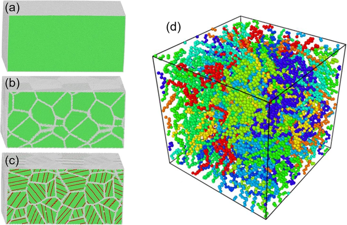
一 单晶铜的显微结构。 b 纳米多晶的显微结构。 c NT多晶的显微结构。原子根据 CNA 值着色,因为绿色和白色代表 FCC 和缺陷原子 [25]。 d 无定形PE的平衡联合原子模型,该模型由不同的分子链着色[26]
在之前的研究中,聚合物是用通用粗粒度模型建模的 [37, 38]。例如,建立聚乙烯(PE)模型的细节如下[39]:(i)使用蒙特卡罗自回避随机游走算法获得具有10条分子链的初始PE系统[39]; (ii) 每条链的第一个原子首先插入晶格的可用位点,然后分子链开始根据键长和单元格中未占据位点的概率逐步方式沿某个方向生长.; (iii) 一旦给定了初始密度,就确定了模拟框的大小。在我们的模拟中,初始模拟框的尺寸约为 80.06 × 80.06 × 80.06 Å 3 对于由 10 个 PE 链组成的系统。 PE的MD模型如图1d所示。
尖端几何形状通常复杂多变,包括锥形 [40]、三棱锥 [18] 和半球(钝形)[21],这在 TBN 工艺中起着重要作用。特别是MD模型中金字塔刀具的形状与AFM加工过程中的形状一致,球形刀具与磨削过程中的磨粒一致;因此,通过将模拟结果与实验结果进行比较,可以更好地解释加工机制。在大多数情况下,尖端被认为是无限刚性的,这是通过保持原子的相对位置恒定并以恒定速度移动来实现的[41]。
选择合适的势能函数也很重要,这决定了模拟结果的可信度 [21]。 EAM 是一种适用于金属系统的多体势能 [24]。它提供了对金属内聚力的更现实的描述,并避免了由体积依赖性继承的模糊性,体积依赖性用于描述金属原子之间的相互作用,例如铜 [42] 和铁 [43]。 Tersoff [44] 和 Stillinger-Weber (SW) [45] 势已被证明对于模拟具有金刚石立方结构的材料特别可行。为了研究 TBN 过程中 Si 的机制,应在 MD 模拟中观察位错滑移和相变。与 Tersoff 电位相比,SW 电位不仅具有足够的灵活性来描述许多不同的硅配置,而且还提供了与从头位错成核结果最接近的无缺陷硅匹配 [46, 47]。因此,SW 势函数可能有更多的潜力来描述硅原子之间的相互作用。分析键序势 (ABOP)、反应性经验键序 (REBO) 和自适应分子间反应性经验键序 (AIREBO) 势是一类根据紧束缚近似扩展 Tersoff 势函数并依赖于基本量的势。 48]。 ABOP 电位非常适合硅和碳原子之间的相互作用,用于研究 SiC 过程中的材料变形和去除行为。 REBO 势在碳和碳纳米管模拟中特别受欢迎。 AIREBO 模型的开发是为了克服 REBO 势函数的缺陷,提供比 REBO 项更准确的近似值,并且还增加了对更复杂的相互作用进行建模的能力 [41]。聚苯乙烯样品中的分子间和分子内相互作用由公认的 AIREBO 势[49] 描述。
大多数 MD 模拟是使用大规模原子/分子大规模并行模拟器 (LAMMPS) [50] 进行的。一些复杂的工件模型,如多晶和纳米缠绕多晶材料,可以使用 Atomsk [51] 进行。聚合物的构造,包括原子、键角、不当以及它们的各种类型都是从 Material Studio (MS) [52] 生成的数据文件中获得的。 Open Visualization Tool (OVITO) [53] 和可视化分子动力学 (VMD) [54] 都是可视化模型或加工过程的有用工具。
通过使用 MD 模拟,可以有效地建立各种材料模型。然而,大多数工件模型的尺寸小于 50 nm × 50 nm × 50 nm,这可能会导致与实际结果的偏差 [40, 55, 56]。此外,仍然缺乏可以有效描述一些材料如 GaAs 和 Lu2O3 的潜在函数。因此,MD模型及相关势函数仍需优化以更准确地描述仿真过程。
处理配置
在 TBN 实验中,负载控制模式通常是通过在尖端上施加恒定的法向负载来实现的。这种模式已被证明具有更高的精度,尤其是在倾斜或曲面上进行纳米加工。然而,许多 TBN 过程的 MD 模拟是在位移控制器模式下进行的,这可能导致模拟和实验之间的差异 [18, 57]。因此,一些学者通过直接在探针上施加恒定的法向负载来进行负载控制的纳米划痕过程的MD模拟[20, 58]。在加工过程中,可分为松弛阶段、渗透阶段和刮擦阶段三个部分。此外,由于原子力显微镜 (AFM) 的光束弯曲、具有倾斜角度的基板以及样品表面的粗糙度,尖端不完全垂直于工件。因此,不应忽视尖端倾斜的影响。刘等人。选择具有不同倾斜角度的尖端来研究尖端倾斜对加工结果的影响 [59]。此外,刀尖磨损是加工过程中的关键因素,对加工质量影响较大。水层润滑纳米划痕可减少刀尖磨损,延长刀具寿命,保证加工质量。然而,受水层润滑影响的加工机制仍不清楚。为了解决这一点,Ren 等人。用MD模拟方法研究了水层润滑对单晶铜加工结果的影响[60]。
单划痕工艺已被证明是一种制造纳米凹槽的简单方法,但它对凹槽的尺寸有限制。提出了多道划痕方法来扩大纳米凹槽的尺寸[62]。耿等人。已经通过 MD 模拟和实验结果研究了单通道方法和多通道方法之间的差异 [20]。单程和多程方法都可以被认为是静态犁式光刻,它是用原子力显微镜系统的接触模式进行的。然而,静态犁式光刻在进行长距离刮擦过程时可能会引起不可忽略的尖端磨损。基于攻丝模式的加工技术被称为动力学犁式光刻,它具有减少尖端磨损的潜力。图2分别显示了单晶铜上静态和动态犁形光刻的示意图。对于静态耕作,金刚石尖端首先向下进给,然后开始沿 x 的负方向耕作 轴。犁完后,将尖端向上收回到原来的垂直位置。对于动态耕作过程,金刚石尖端沿着具有尖峰谷振幅和周期的正弦曲线移动 [19]。基于攻丝模式的加工技术原理,Sundaram 等人。开发了一种使用 AFM 的新型纳米加工方法,称为松散磨料 (VANILA) 的振动辅助纳米冲击加工。在该方法中,AFM 用作平台,并将纳米磨料注入硅工件和 AFM 尖端振动之间的浆料中。磨料的动能由 AFM 尖端的振动产生,从而导致样品的纳米级材料去除 [61]。 VANILA工艺示意图如图2b、c所示。
<图片>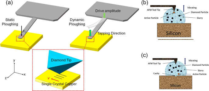
一 单晶铜上静态和动态犁形光刻的示意图[19]。 b AFM 工具尖端撞击金刚石颗粒。 c 金刚石颗粒撞击工件 [61]
模拟结果分析
切削力分析
切削力可以清楚地反映材料去除过程和缺陷的演变,是理解切削现象的重要物理参数[19,63,64]。此外,切削力与切削功率和刀具寿命密切相关,可为TBN加工过程提供指导[65]。在TBN工艺中,切削力主要通过力标定法进行评估,而横向力无法通过这种方法获得[66, 67]。通过使用分子动力学技术,可以实时观察整个过程中切削力的变化,包括横向和切向力[68]。此外,还可以通过MD模拟方法获取平均力和合力。
通过对切削力变化的分析,可以反映出各种材料结构的差异以及加工参数对TBN工艺的影响。李等人。发现与单晶 Cu 相比,在多晶 Cu 上划伤的力更大,这是因为当尖端从一个晶粒到另一个不同晶体取向的晶粒时,表面晶粒的各向异性在工件和尖端之间几乎没有影响,而由于其单取向系统[25],在单晶Cu的材料去除中显示出稳定的塑性流动。还发现不同晶体结构的切割力随着切割速度的增加而增加,因为更高的纳米划痕速度会产生更多的芯片[69]。相反,切削力的变化在 SiC 的划痕过程中表现出不利的行为,因为更高的速度可以产生更多的非晶晶体结构原子,这使得 SiC 材料更具延展性,更容易去除 [70]。严等人。使用 MD 模拟方法研究了 Cu/Ni 双层的可加工性,发现与 Cu、Ni 和双层 Cu-Ni 相比,Ni-Cu 双层的力更高,因为位错的运动受到双层界面的阻碍。作为传播的障碍[71]。关于无定形聚合物,加工性能在以下三个不同方面受到刮擦速度的影响 [72]:首先,在较高速度下产生的尖端前较大的堆积高度导致更大的切向力,因为更多尖端的阻力。然后,更高的速度导致更高的变形率,这可能导致材料的应变硬化。这也会导致切削力的增加。最后,随着速度的增加,热软化效应使工件更容易加工,减少切向力和法向力。在聚合物的加工过程中,切削力随着速度的增加而增加,表明堆积和应变速率硬化效应在决定划痕力方面起着更重要的作用。除了工件材料的影响外,刀尖几何形状在加工过程中也起着重要作用 [18, 73, 74]。任等人。研究了尖端角度对锥形尖端切削力的影响。发现由于尖端和工件材料之间接触面积的增加,力随着半顶角的增加而增加 [21]。此外,摩擦系数随半顶点而显着降低,而硬度增加[75]。
也有学者研究了切削力在特定加工条件下的变化。任等人。分析了水层厚度与刮擦力之间的相关性。划痕力随水层厚度变化的变化如图3所示。 与水层主要起润滑和降低切削力作用的宏观划痕过程不同,与润滑作用相比,水层阻力占主导地位,较厚的水层导致较大的总切削力 [60]。此外,还通过分析硬度(每个原子的法向力)和摩擦系数 [59] 来讨论尖端倾斜的影响。结果表明,法向硬度在向前或向后方向比较敏感,尖端横向倾斜的影响可以忽略不计。此外,倾斜对法向力的影响是摩擦系数变化的主要原因,倾斜对刮擦力的影响远小于对法向力的影响。
<图片>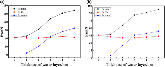
一 平均划痕力随水层厚度变化的变化:a 切向力和 b 法向力 [60]
通过比较静态耕作和动态耕作的切削力,可以揭示机理的不同。动态犁形光刻中的切削力随着金刚石尖端的周期性轻敲而剧烈振荡,而在静态犁形中观察到轻微的波动。此外,动态耕作的平均加工力小于静态耕作的一半,表明动态耕作光刻中的尖端磨损较小[19]。在动态犁刀过程中,刀尖方向对切削力的影响很大。严等人。结合槽深和犁刀力来比较加工效率。结果表明,尖端的侧面向前具有最佳的效率,因为它具有与尖端面向前的方向相似的犁沟力,但同时是凹槽深度的两倍以上 [63]。通过对切削力的分析,可以进一步解释不同材料和加工条件下TBN加工过程的机理。此外,不同加工方式下切削力的比较可为TBN方法的工艺优化提供指导。
材料去除状态分析
材料去除状态分析也是揭示TBN方法机理的重要方法。加工过程中材料和形貌的去除通常通过扫描电子显微镜(SEM)和原子力显微镜观察。然而,凹槽形态和去除状态只能在加工后检测,无法动态了解材料去除过程。最近,张等人。使用直接连接在 SEM 中的线性切削刀具来观察材料切削中的切屑形成过程,而这种方法很复杂,SEM 应进行修改 [76]。因此,这种方法难以推广。与实验方法相比,MD模拟方法可以方便地探索纳米尺度的材料去除机制和表面生成,并且可以通过MD方法实时观察加工过程。
从TBN过程的MD模拟结果可知,变形状态分为犁耕状态和切削状态。随着刀尖的运动,刀尖前方的工件材料原子被挤压,然后在切削状态下积累形成连续切屑。同时,也有一些工件材料原子在通过尖端后堆积在加工凹槽的左右两侧[57]。通过比较切削状态与非切削状态的比值,我们可以得到在不同的划痕深度下使用不同的尖端半径进行划痕时,切削状态还是耕作状态占主导地位[77]。近年来,许多学者进一步研究了材料去除状态下的材料特性。例如,单晶材料在 TBN 工艺中表现出各向异性,这对材料去除有很大影响 [20]。与单晶材料相比,晶界对多晶材料的力学性能有重要影响。高等人。发现晶粒取向而不是晶粒尺寸在确定堆积轮廓方面也占主导地位 [78]。此外,尖端几何形状对材料去除也有很大影响。选择了三种类型的尖端(锥形、三棱锥和半球形尖端)来揭示尖端几何形状对材料去除状态的影响。对于锥形尖端,对半顶角有明显的依赖性。刀尖半顶角越大,切屑量越大,划伤面的光洁度越高,但需要更大的划伤力,在工件中产生更大的摩擦系数和更高的温度,增加亚表面损伤[40]。 Alhafez 还研究了半顶角对堆积形成的影响 [75]。研究发现,在刀尖半顶角较小的情况下,在刀尖半顶角大的加工条件下,堆积多沿前向堆积,而横向堆积占主导地位。一些研究集中在三角锥尖端,它与基于 AFM 的加工过程中尖端的真实几何形状一致 [19, 20, 63, 79]。主要比较了三个加工方向,即边缘向前、正面向前和侧面向前。在碳化硅的加工过程中,可以通过调整刀具的划伤方向来简单地控制材料去除状态。边缘向前的刮擦方向可以提供更稳定的过程,这可以导致获得的凹槽的尺寸精度和一致性更好[79]。然而,与金属或半导体材料相比,聚合物的材料去除状态对温度更敏感。在划痕过程中,划痕区的局部温度高于玻璃化转变温度,这表明划痕区的工件可以以延展的方式去除[72]。詹等人。研究了无定形聚苯乙烯的微观摩擦机制。他们发现分子链的柔韧性随着温度的升高而增加,这可以使分子链更容易卷曲并恢复到原始状态[56]。杜等人。发现加工速度对聚苯乙烯的加工结果有很大影响。聚苯乙烯试样的永久变形在加工速度小时链内变化占主导地位,而加工速度大时链间滑动更明显[80]。
从上面的讨论可以看出,大多数研究主要集中在干燥条件而不是流体上。但是,随着水层厚度的增加,刀具前面堆积的原子减少了,沿凹槽的毛刺不明显,表面粗糙度明显降低,表面相对光滑。可以解释为,水层起到润滑剂的作用,以减少刀具与新形成的切屑表面之间的粘附区域,并减少在切屑-刀具面边界处表现出的拖曳力。直接的后果是大大提高了表面质量。随着水层厚度的增加,表面质量可以逐渐改善[60]。在一些新颖的加工方法中,Shockly 等人。研究了振动辅助纳米冲击加工中参数(冲击速度、冲击角度和工作温度)对纳米腔形成的影响,发现工作参数对所产生的纳米腔的深度和宽度有很大影响,如图所示. 4 [61]。肖等人。发现动态犁沟的深度和宽度小于静态犁沟的深度和宽度,这意味着可以通过动态犁沟光刻制造具有小特征的纳米结构。此外,在动态耕作过程中,通过驱动振幅比可以控制凹槽的尺寸,这表明凹槽的制作也是可控的[19]。
<图片>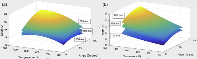
a 的多元线性回归图 纳米腔的深度(冲击速度、冲击角度和工作温度)和 b 纳米腔的宽度(冲击速度、冲击角度和工作温度)[61]
在材料去除过程中,尖端存在磨损行为。在以前的大多数研究中,尖端被定义为刚体,这意味着不能直接观察到刀具磨损现象[13]。许多学者通过研究材料去除状态、应力和温度分布来研究刀具磨损 [70, 77]。为了反映加工过程中刀尖的真实磨损现象,Meng等。将尖端设置为可变形体,并在加工过程中发现了尖端的磨损行为 [81]。结果表明,金刚石磨粒磨损的形式主要是开始阶段的粘着磨损和加工稳定阶段的逐原子磨损,磨料逐原子的磨损量受切削速度的影响较小。 81]。值得注意的是,关于尖端磨损行为的报告相对较少。希望利用尖端的可变形体进一步促进纳米加工过程中尖端磨损行为的研究。
材料去除状态分析为加工过程的实时监控提供了有效支持。然而,由于上述长度尺度的限制,加工表面的形貌和材料去除过程只能通过定性比较来分析。很难预测准确的处理结果。
Defect Evolution Process Analysis
To obtain the information about the defects generated during the scratching process, TEM is usually employed after the FIB sample preparation techniques, which has several disadvantages, such as relatively complicated operation, high cost, and strong material dependence.
The MD simulation method can obtain the defects generated beneath the sample surface easily. Moreover, the defect evolution process during the scratching could also be observed by using the MD simulation approach, which could not be obtained by experimental method. Many available algorithms to extract defect types were presented, including common neither analysis (CNA) [82], centro-symmetry parameter (CSP) [83], slip vector analysis [84], Ackland-Jones analysis [85], etc. However, these methods are not suitable for tracing the propagation of dislocations, especially when a large number of dislocations are generated by tip scratching along certain direction, and we can no longer investigate what is going on inside the specimen using these methods [86].陈等人。 presented slipping analysis for visualizing the atomic slipping process for material deformation, which could filter out those atoms that have slipped relative to its neighbor atoms during a specified period of time in the condition with large numbers of atoms [86]. By using this method, Xiao et al. investigated the slipping process during dynamic and static ploughing lithography [19]. The relationship between the cutting force and slipping process is shown in Fig. 5. It could be seen that for dynamic ploughing, the sample material mainly flows downwards and sidewards, whereas no obvious downwards material flow is observed in static ploughing process. In addition, the propagation of the dislocation is dependent on the orientation of the tip, leading to the various morphologies of the grooves. Dislocation extraction algorithm (DXA) is also a useful dislocation analysis tool to identify the lattice dislocation and to determine their Burger vector [87]. By using this method, Gao et al. investigated the behavior of the nanoscratching of iron. They found that a distinct reorganization of the dislocation network. At the beginning, the plastic zone grows linearly with the scratching length along the path. Then, the dislocation density decreases rapidly after some length dislocation reactions. Plastic activity then is concentrated only on the scratch front. Only few dislocations remain in the middle of the scratch. Vacancies in this zone are created by dislocation reactions. It is also found that point defects vacancies generated by dislocation reactions and deformation twining [88].

Slipping processes in a dynamic ploughing and b static ploughing [19]
For the polycrystalline materials, the deformation mechanism was mediated by dislocation nucleation within grain interior as well as grain boundary dislocations in polycrystalline material [43]. While the dislocation propagation is associated with the formation of nanovoids and interstitial clusters in the case of larger grain size, and the formation of twins at the grain boundary was dominating for smaller clusters. This behavior was attributed to the transition of dislocation movement from smooth (larger grain) to rough (smaller grain) during scratching process. Li further concluded the difference of material deformation mechanism about single crystal Cu, polycrystalline Cu, and NT polycrystalline Cu. The results show that the plastic deformation is mainly affected by the interaction between dislocations during scratching process in single crystal Cu; while for polycrystalline Cu both dislocations and GB dominate the plastic deformation; and the plastic deformation is controlled by the interactions of the dislocation, grain boundary (GB), and twin boundary (TB) accompanied with twinning/detwinning [25].
Furthermore, many studies focused on the MD simulation of the TBN process on the semiconductor materials, such as silicon, silicon carbide, gallium arsenide, and aluminum nitride. To investigate these brittle materials, phase transformation is also an important deformation mode in addition to dislocation slip [89]. The interaction between dislocation and phase transformation varies with the crystal orientation. The results indicate that prior to the “Pop-In” event, Si (010) undergoes inelastic deformation accompanied by the phase transformation from the Si-I to the Si-III/ Si-XII, which is not occurred in Si (110) and Si (111). While, the phase transformation from the Si-I to the bct-5 is the dominant mechanism of incipient plasticity for each crystallographic orientation, and dislocation nucleation is also an operating deformation mode in the elastic-plastic transition of Si (010).戴等人。 investigated the subsurface damage mechanism on single crystal silicon during TBN process. It is found that the evolution of crystalline phases is consistent with the distribution of hydrostatic stress and temperature [40]. SiC is also a kind of important semiconductor material, which has the similar property as silicon. The SiC material removal process is achieved through the phase transfer from zinc blended to amorphous structure with few hexagonal diamond structures. Higher scratching speed generates more amorphous structure atoms, fewer hexagonal diamond atoms, and fewer dislocation atoms due to larger impaction and less rearrangement time [90]. While Meng et al. found when the phase transition is not the dominant deformation mechanism, the Schmidt coefficient method can effectively predict the sliding motion of 3C-SiC during the TBN process (elastic sliding motion and dislocation slip motion) [79]. Moreover, Meng et al. further studied on the strain rate and heat effect on the removal mechanism of SiC. They found that the strain rate effect and the thermal softening effect directly affect the material removal amount and form of the subsurface damage (SSD). The influence of the thermal softening effect on the stress in the processing region under the condition of high strain rate exceeds that of the decrease in the growth rate of the dislocation generation speed. The polycrystalline SiC removal process is dominated by the amorphous phase transition. Furthermore, several hexagonal diamond structure atoms and dislocations are found in the GBs during the scratching. Higher scratching speed and larger depth of cut promotes more atoms to transfer into the amorphous structure due to larger impaction [81]. Compared with monocrystalline SiC, the microstructure in polycrystalline makes the SiC more soften by generating less normal scratching force and amorphous structure phase transition and thinner plastic deformation induced SSD [91]. Dislocation propagation and phase transition analysis could explain the mechanism in machining process. However, most researches focused on single crystalline materials and the materials with complex structure are rarely reported, which should be further studied.
Future Research Directions and Challenges
At present, the research on the TBN process through MD simulation is widely reported. However, there are still some limitations to be considered. Thus, future directions are discussed in this review.
- (1)
With the development of TBN methods, some novel technologies have been proposed in this field. For example, AFM tip-based nanomilling process has a broad prospect due to its great machining performance and size control properties [92, 93]. However, the mechanism of nanomilling has not been fully understood due to limitation of the detection equipment. With the use of MD simulation, it is hopeful that the variation of the cutting force, the dynamics change of defects, and the removal state of workpiece materials during rotating process of the tip. In addition, sample vibration-assisted nanoscratching method has not been reported yet. MD simulation approach could provide meaningful guidance in the early stage.
- (2)
Due to the limitation of the length and time scales, MD methods still could not fully describe the experimental process quantitatively. In some studies combining experiments and MD simulations, MD simulation approach could only qualitatively explain the experimental phenomena [19, 20, 94]. In particular, for some time-dependent materials such as amorphous polymers, the velocity of the probe has a significant impact on the removal state of polymers. Thus, in order to accurately predict the experimental process and quantitative analyze the experimental results, the improvement of algorithm and computing capability is indispensable.
- (3)
Many nanostructures have been achieved on polymer materials using the TBN method [95,96,97]. In particular, the mechanical machining process of polymer materials based on TBN method keeps the normal load constant so as to guarantee the accuracy of the machined nanostructures [98]. However, the reports of MD simulation of polymer in TBN process are limited until now. Moreover, thermal scanning probe lithography is developing in polymer, which has the potential to improve the machining accuracy of the TBN process. It is necessary to reveal the material removal mechanism of the polymer materials when conducting nanoscale scratching process with the mechanical-thermal effect.
结论
It is undeniable that MD simulations technology plays an increasingly crucial role in nanomachining process to reveal hitherto unknown phenomena [99]. This review concluded the recent progress in MD simulation of TBN method, and the above contents are summarized as follows:
- (1)
The establishment of MD models of various materials and related potential function were summarized. In particular, the modeling process of NT polycrystalline materials and amorphous polymers were discussed in this section. The accuracy of MD models is of great significant to the subsequent simulation results.
- (2)
The new technologies of TBN methods, including multi-scratching, dynamic ploughing, and VANILA were presented. With the help of MD simulation, the mechanism of these methods could be better understood. In particular, the essential difference between static ploughing and dynamic ploughing was revealed by MD method from the aspects of internal defects, morphology and cutting forces.
- (3)
The analysis of MD simulations in TBN process, including the cutting force, the state of material removal, and defect analysis are also summarized. Besides, some novel analysis methods like slipping analysis are also given. With these methods, the processing mechanism based on TBN approach is reviewed, which shows the materials dependence on the TBN machining process.
缩写
- TBN:
-
Tip-based nanomachining
- 原子力显微镜:
-
原子力显微镜
- MD:
-
分子动力学
- NT:
-
Nanotwined
- PE:
-
聚乙烯
- EAM:
-
Embedded atom method
- SW:
-
Stillinger-Weber
- ABOP:
-
Analytical bond order potential
- REBO:
-
Reactive Empirical Bond Order
- AIREBO:
-
Adaptive Intermolecular Reactive Empirical Bond Order
- LAMMPS:
-
大规模原子/分子大规模并行模拟器
- MS:
-
Material studio
- OVITO:
-
打开可视化工具
- VMD:
-
Visual molecular dynamics
- VANILA:
-
Vibration-Assisted Nano Impact machining by Loose Abrasives
- SEM:
-
扫描电子显微镜
- CNA:
-
Common neighbor analysis
- CSP:
-
Centro-symmetry parameter
- DXA:
-
Dislocation extraction algorithm
- GB:
-
Grain boundary
- 结核病:
-
Twin boundary
- SSD:
-
Subsurface damage
纳米材料