

微通道板上偶氮导电层的设计
摘要
当AZO导电层的电阻率在MCP电阻要求范围内时,Zn含量的区间很窄(70-73%),难以控制。针对微通道板上AZO导电层的特性,设计了一种算法来调整导电材料ZnO和高阻材料Al2O3的比例。我们提出了MCP工作电阻的概念(即微通道中电子雪崩时的电阻)。采用MCP电阻测试系统首次测量了AZO-ALD-MCP(Al2O3/ZnO原子层沉积微通道板)的工作电阻。与常规MCP相比,我们发现AZO-ALD-MCP在工作状态和非工作状态下的电阻有很大差异,并且随着电压的增加,工作电阻显着降低。因此,我们提出了一套针对导电层的分析方法。我们还提出在工作电阻条件下调整ALD-MCP导电层的导电材料与高阻材料的比例,成功制备了高增益AZO-ALD-MCP。该设计为寻找更好的ALD-MCP导电层材料以提高MCP的性能开辟了道路。
介绍
微通道板 (MCP) 是一种电子倍增器,由薄玻璃板形式集成的二维孔阵列组成,长度为 0.5-5 毫米,直径为 4-40 微米,与法线的偏角通常为 5°-13°板面;板材开孔率高达60%,各孔长径比高,约为20:1~100:1[1]。
如图 1 所示,进入微通道的入射电子与壁碰撞,导致在微通道壁表面产生二次电子。与微通道壁的多次碰撞将导致二次电子数量的增加,从而导致微通道内的电子雪崩和从微通道输出端发射出一团电子。二次电子将通过偏置电压沿微通道进一步加速。 MCP增益为10 3 –10 4 工作电压为 700–900 V [2,3,4,5,6,7,8,9]。
<图片>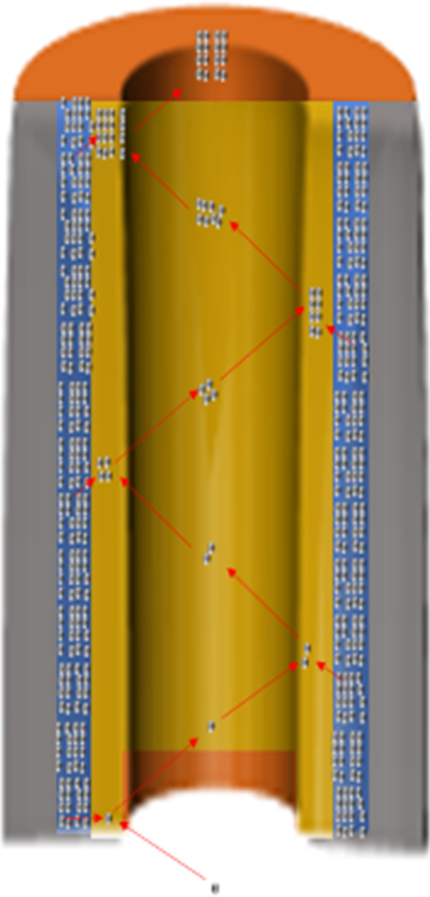
MCP工作状态图
每个微通道作为检测器和电子倍增器。 MCP具有数百万条独立工作的微通道,具有空间分辨率高、时间分辨率高、增益范围广等特点,用于识别光子、电子、中子和离子。 MCP可以集成到各种仪器中,包括光电探测器、光电倍增管(PMT)、紫外光谱仪、阴极射线管、扫描电子显微镜、场发射显示器、残留气体分析仪、医学成像、飞行时间质谱、夜间-视力护目镜等 [1, 4, 7,8,9]。传统工艺的氢气烧制使得微通道具有合适的电导率和二次电子发射系数。
微通道制备中常用的烧氢工艺存在很多不足:首先,烧氢工艺不能独立调整导电层和发射层[10, 11];二是铅玻璃冶炼过程中的重金属元素(Pb、Bi)导致环境污染;第三,大面积的MCP会因高温而翘曲[8];第四,使用氢还原反应的铅玻璃含有K、Rb等放射性元素,产生背景噪声[8];最后,残留在孔隙中的氢在偏压作用下变成离子,向与电子相反的方向飞行,破坏仪器的阴极[8, 12]。
早期的科学家提出了一种在微通道壁上生长导电层和发射层的解决方案,以取代氢气烧制过程[3]。许多薄膜沉积方法无法在高长径比的微通道中生长均匀的薄膜。阿贡国家实验室提出使用原子层沉积 (ALD) 在 MCP 上生长导电层和发射层,以在微通道壁上实现完整且均匀的薄膜 [4, 13]。此外,ALD-MCP 解决了上述缺点。许多研究机构都致力于寻找可以提高MCP性能的有竞争力的材料。
阿贡国家实验室考虑到 MCP 电阻要求,为 ALD-MCP 导电层选择 AZO 材料。如果电阻太高,导电层不能及时、持续地向发射层补充电子,MCP就会出现低增益甚至无法工作。另一方面,如果电阻太低,MCP 会过热,最终导致击穿 [4, 9, 14, 15]。因此,导电层的设计对于ALD-MCP具有重要意义。
如图 2 所示,当 AZO 导电层的电阻率在 MCP 电阻要求范围内时,允许的 Zn 含量在非常窄的范围内 (70-73%) [16]。因此,MCP 增益不稳定,MCP 很容易击穿。已经研究了替代导电材料如 W 和 Mo 代替 Zn [3, 4, 17,18,19]。 \({\text{WF}}_{6}\) (\({\text{MoF}}_{6}\)) 和 \({\text{H}}}_{2} 的化学反应{\text{O}}\) 用于通过 ALD 生长 W (Mo)。然而,使用 \({\text{WF}}}_{6}\) 或 \({\text{MoF}}_{6}\) 有两个严重的缺点:它们具有很强的腐蚀性,并且它们含有杂质,这些杂质可以生产过程中难以去除。由于这些原因,使用这些材料的 ALD-MCP 成本很高。
<图片>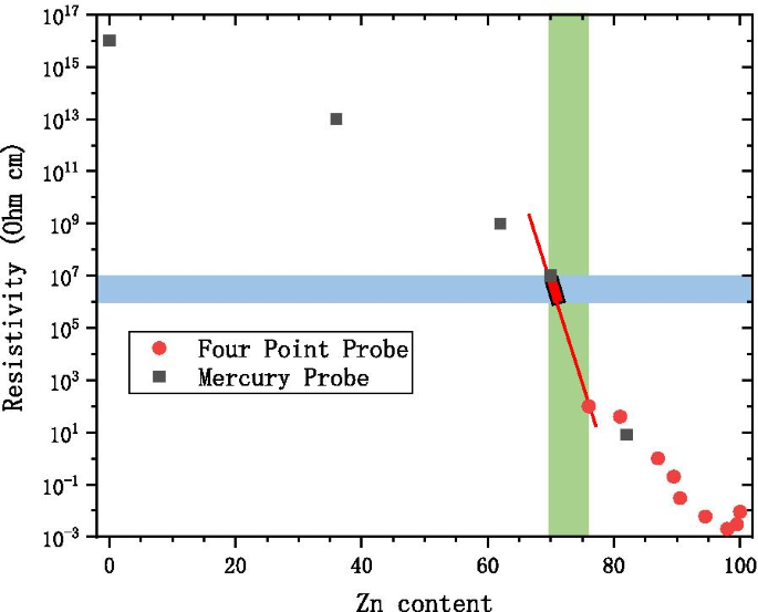
Zn含量,Zn/(Zn + A)*100(%),蓝色区域为MCP电阻区域,绿色区域为AZO变化区域,红色区域为需要控制的区域
在我们的研究中,我们发现可以为 MCP 导电层实现 ZnO 和 \({\text{Al}}_{2} {\text{O}}_{3}\) 的合理设计,而没有挑战如果使用 W 或 Mo 则面临,并且在价格上更具竞争力。在此,我们将具有偶氮导电层的ALD-MCP命名为AZO-ALD-MCP。
我们提出了一种算法来调整导电材料 ZnO 和高电阻材料的比例 \({\text{Al}}_{2} {\text{O}}_{3}\) 以获得我们想要的 AZO 导电层特性。
我们提出了MCP工作电阻的概念(即微通道中电子雪崩时的电阻)。我们测试了 AZO-ALD-MCP 的工作电阻,发现 AZO-ALD-MCPs 和传统 MCPs 之间存在两个差异。我们观察到 AZO-ALD-MCPs 和传统 MCPs 的工作和非工作电阻显着不同。此外,AZO-ALD-MLP 的电阻与电压呈负相关。我们关于调整导电材料和高电阻材料比例的建议(工作电阻参考)提供了指导,帮助我们寻找用于 ALD-MCP 导电层的新材料,以提高其性能。未来的 MCP。
实验和方法
生长氧化锌和\({\text{Al}}_{2} {\text{O}}_{3}\) 原子膜
原子层沉积 (ALD) 是一种将前体和反应气体交替到基材表面以进行物理或化学吸附或以受控速率进行表面饱和反应的技术。该材料以单原子薄膜表面的形式沉积在基板上。 ALD可以生产无针孔的连续薄膜,具有优良的覆盖率,并且可以控制原子薄膜的厚度和成分[1, 2, 4, 11, 13, 19, 20]。
以下是使用ALD生长Al2O3的化学反应方程式:
$$\begin{aligned} &{\text{A}}:{\text{Substrate}} - {\text{OH}}^{*} + {\text{Al}}\left( {{\text {CH}}_{3} } \right)_{3} \\ &\quad \to {\text{Substrate}} - {\text{O}} - {\text{Al}}\left( { {\text{CH}}_{3} } \right)_{2}^{*} + {\text{CH}}_{4} \uparrow \\ &{\text{B}}:{\ text{Substrate}} - {\text{O}} - {\text{Al}}\left( {{\text{CH}}_{3} } \right)_{2}^{*} + 2 {\text{H}}_{2} {\text{O}} \\ &\quad \to {\text{Substrate}} - {\text{O}} - {\text{Al}}\left ( {{\text{OH}}} \right)_{2}^{*} + 2{\text{CH}}_{4} \uparrow \\ &{\text{C}}:{\text {Al}} - {\text{OH}}^{*} + {\text{Al}}\left( {{\text{CH}}_{3} } \right)_{3} \\ { } &\quad \to {\text{Al}} - {\text{O}} - {\text{Al}}\left( {{\text{CH}}_{3} } \right)_{ 2}^{*} + {\text{CH}}_{4} \uparrow \\ &{\text{D}}:{\text{Al}} - {\text{CH}}_{3} ^{*} + {\text{H}}_{2} {\text{O}} \to {\text{Al}} - {\text{OH}}^{*} + 2{\text{ CH}}_{4} \uparrow \\ \end{对齐}$$反应温度为 60–150 °C。如图3所示,生长一层Al2O3原子的时间和顺序为:
<图片>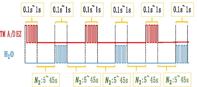
生长Al2O3和ZnO图
\({\text{TMA}}/{\text{N}}_{2} /{\text{H}}_{2} {\text{O}}/{\text{N}}_{ 2} =0.1\sim1{\text{s}}/5\sim45{\text{s}}/0.1\sim1{\text{s }}/5\sim45{\text{s}}\).
以下是使用ALD生长ZnO的化学反应方程式:
$$\begin{aligned} &{\text{E}}:{\text{Substrate}} - {\text{OH}}^{*} + {\text{Zn}}\left( {{\text {CH}}_{2} {\text{CH}}_{3} } \right)_{2} \\ &\quad \to {\text{Substrate}} - {\text{O}} - {\text{ZnCH}}_{2} {\text{CH}}_{3}^{*} + {\text{CH}}_{3} {\text{CH}}_{3} \ uparrow \\ &{\text{F}}:{\text{Substrate}} - {\text{O}} - {\text{ZnCH}}_{2} {\text{CH}}_{3} ^{*} + {\text{H}}}_{2} {\text{O}} \\ &\quad \to {\text{Substrate}} - {\text{O}} - {\text{ ZnOH}}^{*} + {\text{CH}}_{3} {\text{CH}}_{3} \uparrow \\ &{\text{G}}:{\text{Zn}} - {\text{OH}}^{*} + {\text{Zn}}\left( {{\text{CH}}_{2} {\text{CH}}_{3} } \right) _{2} \\ &\quad \to {\text{Zn}} - {\text{O}} - {\text{ZnCH}}_{2} {\text{CH}}_{3}^ {*} + {\text{CH}}}_{3} {\text{CH}}_{3} \uparrow \\ &{\text{H}}:{\text{Zn}} - {\text {CH}}_{2} {\text{CH}}_{3}^{*} + {\text{H}}_{2} {\text{O}} \to {\text{Zn} } - {\text{OH}}^{*} + {\text{CH}}_{3} {\text{CH}}_{3} \uparrow \\ \end{aligned}$$反应温度为 60–150 °C。如图3所示,生长一层ZnO原子的时间和顺序为:
$${\text{DEZ}}/{\text{N}}_{2} /{\text{H}}_{2} {\text{O}}/{\text{N}}_{ 2} =0.1\sim1{\text{s}}/5\sim45{\text{s}}/0.1\sim1{\text{s }}/5\sim45{\text{s}}{.}$ $偶氮导电层的设计
AZO 的厚度通常在 300 到 1000 个原子层之间。我们定义了一个新的数学运算规则来设计Al2O3和ZnO的原子层序,以调整导电材料ZnO和高阻材料Al2O3的比例。
$$\left(\begin{array}{*{20}c} {{\text{mA}}} \\ {{\text{mB}}} \\ \vdots \\ \end{array} \right )={\text{m}}\left(\begin{array}{*{20}c} {\text{A}} \\ {\text{B}} \\ \vdots \\ \end{array }\right)$$ (1) $$\begin{aligned} &{\text{A}}\left(\begin{array}{*{20}c} {\text{a}} \\ {\ text{b}} \\ \vdots \\ \end{array}\right) + {\text{B}}\left(\begin{array}{*{20}c} {\text{c}} \ \ {\text{d}} \\ \vdots \\ \end{array}\right) + {\text{C}}\left(\begin{array}{*{20}c} {\text{e }} \\ {\text{f}} \\ \vdots \\ \end{array}\right) \ldots \\ &\quad =\left(\begin{array}{*{20}c} {\ text{A}} \\ {\text{B}} \\ \vdots \\ \end{array}\right) \left[ \left(\begin{array}{*{20}c} {\text{ a}} \\ {\text{b}} \\ \vdots \\ \end{array}\right) \left(\begin{array}{*{20}c} {\text{c}} \\ {\text{d}} \\ \vdots \\ \end{array}\right) \left(\begin{array}{*{20}c} {\text{e}} \\ {\text{f }} \\ \vdots \\ \end{array}\right) \ldots \right] =\left(\begin{array}{*{20}c} {{\text{Aa}} + {\text{ Bc}} + {\text{Ce}} + \ldots } \\ {{\text{Ab}} + {\text{Bd}} + {\text{Cf}} + \ldots } \\ \vdots \\ \end{array}\right) \\ \end{aligned}$$ (2)数学运算被命名为 WYM 运算。 WYM 操作有两个属性和一个公式。
WYM 属性 1:
$$\begin{aligned} &\left( {\begin{array}{*{20}c} {\text{m}} \\ {\text{n}} \\ \end{array} } \right )\left[ {\left( {\begin{array}{*{20}c} {\text{a}} \\ {\text{b}} \\ \end{array} } \right)\left ( {\begin{array}{*{20}c} {\text{c}} \\ {\text{d}} \\ \end{array} } \right)} \right]\left[ {\ left( {\begin{array}{*{20}c} {\text{e}} \\ {\text{f}} \\ \end{array} } \right)\left( {\begin{array }{*{20}c} {\text{g}} \\ {\text{h}} \\ \end{array} } \right)} \right]\left[ {\left( {\begin{数组}{*{20}c} {\text{i}} \\ {\text{j}} \\ \end{array} } \right)\left( {\begin{array}{*{20} c} {\text{k}} \\ {\text{l}} \\ \end{array} } \right)} \right] \ldots \\ &\quad =\left( {\begin{array} {*{20}c} {\text{m}} \\ {\text{n}} \\ \end{array} } \right)\left\{ {\left( {\begin{array}{* {20}c} {\text{a}} \\ {\text{b}} \\ \end{array} } \right)\left[ {\left( {\begin{array}{*{20} c} {\text{e}} \\ {\text{f}} \\ \end{array} } \right)\left( {\begin{array}{*{20}c} {\text{g }} \\ {\text{h}} \\ \end{array} } \right)} \right],\left( {\beg in{array}{*{20}c} {\text{c}} \\ {\text{d}} \\ \end{array} } \right)\left[ {\left( {\begin{array }{*{20}c} {\text{e}} \\ {\text{f}} \\ \end{array} } \right)\left( {\begin{array}{*{20}c } {\text{g}} \\ {\text{h}} \\ \end{array} } \right)} \right]} \right\}\left[ {\left( {\begin{array} {*{20}c} {\text{i}} \\ {\text{j}} \\ \end{array} } \right)\left( {\begin{array}{*{20}c} {\text{k}} \\ {\text{l}} \\ \end{array} } \right)} \right] \ldots \\ &\quad =\left( {\begin{array}{* {20}c} {\text{m}} \\ {\text{n}} \\ \end{array} } \right)\left[ {\left( {\begin{array}{*{20} c} {\text{a}} \\ {\text{b}} \\ \end{array} } \right)\left( {\begin{array}{*{20}c} {\text{c }} \\ {\text{d}} \\ \end{array} } \right)} \right]\left\{ {\left( {\begin{array}{*{20}c} {\text {e}} \\ {\text{f}} \\ \end{array} } \right)\left[ {\left( {\begin{array}{*{20}c} {\text{i} } \\ {\text{j}} \\ \end{array} } \right)\left( {\begin{array}{*{20}c} {\text{k}} \\ {\text{ l}} \\ \end{array} } \right)} \right],\left( {\begin{array}{*{20}c} {\te xt{g}} \\ {\text{h}} \\ \end{array} } \right)\left[ {\left( {\begin{array}{*{20}c} {\text{i }} \\ {\text{j}} \\ \end{array} } \right)\left( {\begin{array}{*{20}c} {\text{k}} \\ {\text {l}} \\ \end{array} } \right)} \right]} \right\} \ldots \\ \end{aligned}$$WYM 属性 2:
$$\begin{aligned} &{\text{A}}\left( {\begin{array}{*{20}c} {\text{m}} \\ {\text{n}} \\ \ end{array} } \right)\left[ {\left( {\begin{array}{*{20}c} {\text{a}} \\ {\text{b}} \\ \end{array } } \right)\left( {\begin{array}{*{20}c} {\text{c}} \\ {\text{d}} \\ \end{array} } \right)} \ right]\left[ {\left( {\begin{array}{*{20}c} {\text{e}} \\ {\text{f}} \\ \end{array} } \right)\ left( {\begin{array}{*{20}c} {\text{g}} \\ {\text{h}} \\ \end{array} } \right)} \right] \ldots \\ &\quad =\left( {\begin{array}{*{20}c} {{\text{Am}}} \\ {{\text{An}}} \\ \end{array} } \right )\left[ {\left( {\begin{array}{*{20}c} {\text{a}} \\ {\text{b}} \\ \end{array} } \right)\left ( {\begin{array}{*{20}c} {\text{c}} \\ {\text{d}} \\ \end{array} } \right)} \right]\left[ {\ left( {\begin{array}{*{20}c} {\text{e}} \\ {\text{f}} \\ \end{array} } \right)\left( {\begin{array }{*{20}c} {\text{g}} \\ {\text{h}} \\ \end{array} } \right)} \right] \ldots \\ &\quad =\left( {\begin{array}{*{20}c} {\text{m}} \\ {\text{n}} \\ \end{a rray} } \right)\left[ {{\text{A}}\left( {\begin{array}{*{20}c} {\text{a}} \\ {\text{b}} \ \ \end{array} } \right),{\text{A}}\left( {\begin{array}{*{20}c} {\text{c}} \\ {\text{d}} \\ \end{array} } \right)} \right]\left[ {\left( {\begin{array}{*{20}c} {\text{e}} \\ {\text{f} } \\ \end{array} } \right)\left( {\begin{array}{*{20}c} {\text{g}} \\ {\text{h}} \\ \end{array } } \right)} \right] \ldots \\ &\quad =\left( {\begin{array}{*{20}c} {\text{m}} \\ {\text{n}} \ \ \end{array} } \right)\left[ {\left( {\begin{array}{*{20}c} {\text{a}} \\ {\text{b}} \\ \end {array} } \right)\left( {\begin{array}{*{20}c} {\text{c}} \\ {\text{d}} \\ \end{array} } \right) } \right]\left[ {{\text{A}}\left( {\begin{array}{*{20}c} {\text{e}} \\ {\text{f}} \\ \ end{array} } \right),{\text{A}}\left( {\begin{array}{*{20}c} {\text{g}} \\ {\text{h}} \\ \end{array} } \right)} \right] \ldots \\ \end{aligned}$$WYM公式:
$$\begin{aligned} &\left(\begin{array}{*{20}c} {\text{a}} \\ {\text{b}} \\ \vdots \\ \end{array} \right) =\left(\begin{array}{*{20}c} {{\text{A}} + \frac{{\text{X}}}{{\text{Y}}}} \ \ {\text{b}} \\ \vdots \\ \end{array}\right) \propto {\text{Y}}\left(\begin{array}{*{20}c} {{\text {A}} + \frac{{\text{X}}}{{\text{Y}}}} \\ {\text{b}} \\ \vdots \\ \end{array}\right) =\left( {\begin{array}{*{20}c} {{\text{Y}} - {\text{X}}} \\ {\text{X}} \\ \end{array} } \right)\left[ \left(\begin{array}{*{20}c} {\text{A}} \\ {\text{b}} \\ \vdots \\ \end{array}\right ) \left(\begin{array}{*{20}c} {{\text{A}} + 1} \\ {\text{b}} \\ \vdots \\ \end{array} \right) \right] \\ &\left(\begin{array}{*{20}c} {\text{a}} \\ {\text{b}} \\ \vdots \\ \end{array}\right ) =\left(\begin{array}{*{20}c} {\text{a}} \\ {{\text{B}} + \frac{{\text{X}}}{{\text {Y}}}} \\ \vdots \\ \end{array}\right) \propto {\text{Y}}\left(\begin{array}{*{20}c} {\text{a} } \\ {{\text{B}} + \frac{{\text{X}}}{{\text{Y}}}} \\ \vdots \\ \end{array}\right) =\left( {\begin{array}{*{20}c} {{\text{Y}} - {\text{X}}} \\ {\text{X}} \\ \end{array} } \right)\left[ \left(\begin{array}{*{20}c} {\text{a}} \\ {\text{B}} \\ \vdots \\ \end{array}\right ) \left(\begin{array}{*{20}c} {\text{a}} \\ {{\text{B}} + 1} \\ \vdots \\ \end{array}\right) \right] \\ \end{对齐}$$注意,小写字母代表实数,大写字母代表整数。在示例 1 和示例 2 中,我们展示了操作的执行。
示例 1
$$\left( {\begin{array}{*{20}c} {{\text{ZnO}}} \\ {{\text{Al}}_{2} {\text{O}}_{ 3} } \\ \end{array} } \right) =\left( {\begin{array}{*{20}c} {4 + \frac{1}{2}} \\ 1 \\ \end {array} } \right) \propto \left( {\begin{array}{*{20}c} 1 \\ 1 \\ \end{array} } \right)\left[ {\left( {\begin {array}{*{20}c} 4 \\ 1 \\ \end{array} } \right)\left( {\begin{array}{*{20}c} 5 \\ 1 \\ \end{数组} } \right)} \right] =\left( {\begin{array}{*{20}c} 4 \\ 1 \\ \end{array} } \right) + \left( {\begin{数组}{*{20}c} 5 \\ 1 \\ \end{array} } \right)$$该操作被解释为有两种方案:\(\left( {\begin{array}{*{20}c} 4 \\ 1 \\ \end{array} } \right)\) 和 \(\left( {\begin{array}{*{20}c} 5 \\ 1 \\ \end{array} } \right)\)。对于第一种方案,生长 4 倍 ZnO 原子层和一个 Al2O3 原子层。对于第二种方案,生长 5 倍 ZnO 原子层和一个 Al2O3 原子层。如果我们将这两个方案重复两次,我们将获得如图 4 所示的结构。
<图片>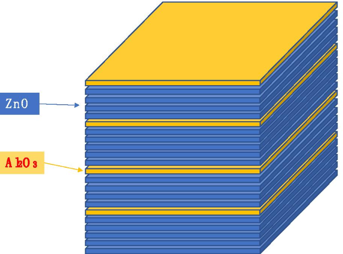
ZnO和Al2O3生长顺序示意图
更复杂的操作规则用法如例2所示,如下:
$$\begin{aligned} &\left( {\begin{array}{*{20}c} {{\text{ZnO}}} \\ {{\text{Al}}_{2} {\text {O}}_{3} } \\ \end{array} } \right) =\left( {\begin{array}{*{20}c} {4.71} \\ 1 \\ \end{array} } \right) =\left( {\begin{array}{*{20}c} {4 + 0.71} \\ 1 \\ \end{array} } \right) \\ &\frac{2}{3 } =0.666 <0.71 <\frac{3}{4} =0.75 \\ &\left( {\begin{array}{*{20}c} E \\ F \\ \end{array} } \right) \left[ {\left( {\begin{array}{*{20}c} {4 + \frac{2}{3}} \\ 1 \\ \end{array} } \right)\left( { \begin{array}{*{20}c} {4 + \frac{3}{4}} \\ 1 \\ \end{array} } \right)} \right] \\ &\quad =E\ left( {\begin{array}{*{20}c} {4 + \frac{2}{3}} \\ 1 \\ \end{array} } \right) + F\left( {\begin{ array}{*{20}c} {4 + \frac{3}{4}} \\ 1 \\ \end{array} } \right) =\left( {\begin{array}{*{20} c} {4E + 4F + \frac{2}{3}E + \frac{3}{4}F} \\ {E + F} \\ \end{array} } \right) \\ &\quad =E + F\left( {\begin{array}{*{20}c} {4 + \frac{{\frac{2}{3}E + \frac{3}{4}F}}{E + F}} \\ 1 \\ \end{array} } \right) \propto \left( {\begin{array}{* {20}c} {4 + \frac{{\frac{2}{3}E + \frac{3}{4}F}}{E + F}} \\ 1 \\ \end{array} } \right) =\left( {\begin{array}{*{20}c} {4.71} \\ 1 \\ \end{array} } \right) \\ &\frac{{\frac{2}{ 3}E + \frac{3}{4}F}}{E + F} =0.71 \Rightarrow {\text{E}} =12,{\text{F}} =13 \\ &\left( { \begin{array}{*{20}c} E \\ F \\ \end{array} } \right) =\left( {\begin{array}{*{20}c} {12} \\ { 13} \\ \end{array} } \right) =12\left( {\begin{array}{*{20}c} 1 \\ {1\frac{1}{12}} \\ \end{数组} } \right) =\left( {\begin{array}{*{20}c} {11} \\ 1 \\ \end{array} } \right)\left[ {\left( {\begin {array}{*{20}c} 1 \\ 1 \\ \end{array} } \right)\left( {\begin{array}{*{20}c} 1 \\ 2 \\ \end{数组} } \right)} \right] \\ &\left( {\begin{array}{*{20}c} E \\ F \\ \end{array} } \right)\left[ {\left ( {\begin{array}{*{20}c} {4 + \frac{2}{3}} \\ 1 \\ \end{array} } \right),\left( {\begin{array} {*{20}c} {4 + \frac{3}{4}} \\ 1 \\ \end{array} } \right)} \right] \\ &\quad =\left( {\begin{数组}{*{20}c} E \\ F \\ \end{array} } \right)\left[ { \left( {\begin{array}{*{20}c} 1 \\ 2 \\ \end{array} } \right)\left[ {\left( {\begin{array}{*{20}c} } 4 \\ 1 \\ \end{array} } \right)\left( {\begin{array}{*{20}c} 5 \\ 1 \\ \end{array} } \right)} \right ],\left( {\begin{array}{*{20}c} 1 \\ 3 \\ \end{array} } \right)\left[ {\left( {\begin{array}{*{20 }c} 4 \\ 1 \\ \end{array} } \right)\left( {\begin{array}{*{20}c} 5 \\ 1 \\ \end{array} } \right)} \right]} \right] \\ &\left( {\begin{array}{*{20}c} {4.71} \\ 1 \\ \end{array} } \right) \propto \left( {\ begin{array}{*{20}c} {12} \\ {13} \\ \end{array} } \right)\left[ {\left( {\begin{array}{*{20}c} 1 \\ 2 \\ \end{array} } \right)\left( {\begin{array}{*{20}c} 1 \\ 3 \\ \end{array} } \right)} \right] \left[ {\left( {\begin{array}{*{20}c} 4 \\ 1 \\ \end{array} } \right)\left( {\begin{array}{*{20}c } 5 \\ 1 \\ \end{array} } \right)} \right] =\left( {\begin{array}{*{20}c} {11} \\ 1 \\ \end{array} } \right)\left[ {\left( {\begin{array}{*{20}c} 1 \\ 1 \\ \end{array} } \right)\left( {\begin{array}{* {20}c } 1 \\ 2 \\ \end{array} } \right)} \right]\left[ {\left( {\begin{array}{*{20}c} 1 \\ 2 \\ \end{array } } \right)\left( {\begin{array}{*{20}c} 1 \\ 3 \\ \end{array} } \right)} \right]\left[ {\left( {\begin {array}{*{20}c} 4 \\ 1 \\ \end{array} } \right)\left( {\begin{array}{*{20}c} 5 \\ 1 \\ \end{数组} } \right)} \right] \\ \end{对齐}$$计划 1 :\(\left( {\begin{array}{*{20}c} {4.71} \\ 1 \\ \end{array} } \right) \propto 12\left[ {\left( {\begin{ array}{*{20}c} 4 \\ 1 \\ \end{array} } \right) + 2\left( {\begin{array}{*{20}c} 5 \\ 1 \\ \end {array} } \right)} \right] + 13\left[ {\left( {\begin{array}{*{20}c} 4 \\ 1 \\ \end{array} } \right) + 3 \left( {\begin{array}{*{20}c} 5 \\ 1 \\ \end{array} } \right)} \right]\).
计划 2 \(\left( {\begin{array}{*{20}c} {4.71} \\ 1 \\ \end{array} } \right) \propto 11\left[ {\left[ {\left( { \begin{array}{*{20}c} 4 \\ 1 \\ \end{array} } \right) + 2\left( {\begin{array}{*{20}c} 5 \\ 1 \ \ \end{array} } \right)} \right] + \left[ {\left( {\begin{array}{*{20}c} 4 \\ 1 \\ \end{array} } \right) + 3\left( {\begin{array}{*{20}c} 5 \\ 1 \\ \end{array} } \right)} \right]} \right] + \left[ {\left[ { \left( {\begin{array}{*{20}c} 4 \\ 1 \\ \end{array} } \right) + 2\left( {\begin{array}{*{20}c} 5 \\ 1 \\ \end{array} } \right)} \right] + 2\left[ {\left( {\begin{array}{*{20}c} 4 \\ 1 \\ \end{array } } \right) + 3\left( {\begin{array}{*{20}c} 5 \\ 1 \\ \end{array} } \right)} \right]} \right]\).
在例2中,Plan 1中的操作可以解释如下:
方案一 ALD生长4次ZnO原子层生长过程和一次\({\text{Al}}_{2} {\text{O}}}_{3}\)原子层生长过程; ALD生长5次ZnO原子层生长过程和一次\({\text{Al}}_{2} {\text{O}}_{3}\)原子层生长过程,并重复两次。
方案二 ALD生长4次ZnO原子层生长过程和一次\({\text{Al}}_{2} {\text{O}}}_{3}\)原子层生长过程; ALD生长5次ZnO原子层生长过程和1次\({\text{Al}}_{2} {\text{O}}_{3}\)原子层生长过程,重复3次。
方案一重复12次,方案二重复13次。
方案二的操作解释与方案一一致。
微通道板电阻测试
如图 5a 所示,我们使用原子层沉积技术在上面生长 AZO 导电层和 \({\text{Al}}}_{2} {\text{O}}_{3}\) 发射层二维孔阵列的微通道壁。然后我们使用热蒸发技术在MCP的两侧生长Ni-Cr电极层[2, 4],并将电极环放在MCP的两侧。为以上准备工作,我们直接测试ALD-MCP电阻。在这种情况下,我们将相应的 MCP 电阻定义为 MCP 的非工作电阻。我们使用 Keithley 6517B 型静电计在 10 −3 中测量 MCP 的非工作电阻 –10 -5 Pa真空[1, 4, 13]。
<图片>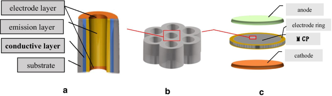
ALD-MCP电阻测试示意图
如图 5c 所示,我们使用电子枪作为阴极,使用荧光屏作为阳极。电子枪向MCP提供入射电子,荧光屏接收MCP输出的电子。此外,当MCP工作时,高压荧光屏会发出绿光来检测MCP的均匀性[1, 21]。
如图 1 所示,我们使用提供 100 pA 作为 MCP 输入的电子枪来测量电流。由于二次电子数量的增加,会出现发射层失去大量电荷,导电层不断向发射层提供电荷流的情况。在这种情况下,我们将相应的 MCP 电阻定义为 MCP 的工作电阻。工作电阻真空环境为10 -3 –10 -5 帕
结果与讨论
AZO-ALD-MCP 样品的横截面 SEM 图片如图 6 所示。我们设计了一系列 AZO 导电层,如表 1 所示,它们对应的工作电阻和非工作电阻如图 7 所示。同样的图,我们还显示了传统 MCP 的工作和非工作电阻。与AZO-ALD-MCP的非工作阻力相比,AZO-ALD-MCP的工作阻力显着降低。然而,传统MCP的工作阻力和非工作阻力之间没有显着差异。随着电压的升高,AZO-ALD-MCP的工作电阻明显低于传统MCP。在相同的电压条件下,AZO-ALD-MCP的工作和非工作电阻是稳定的。我们认为造成上述特点的主要原因有两个。
<图片>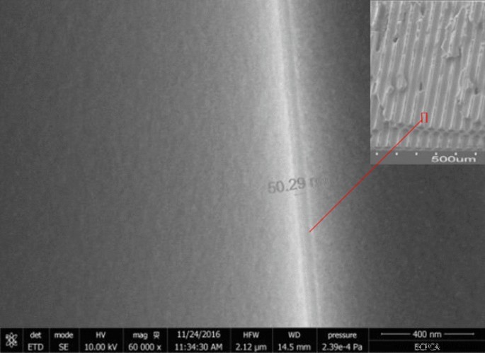
AZO-ALD-MCP的横截面SEM照片
<图片>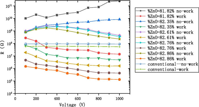
不同比例的AZO-ALD-MCP与常规-MCP的工作电阻和非工作电阻与电压图
根据公式[21],
$$R_{{{\text{MCP}}}} =R_{0} \exp \left[ { - \beta_{T} \left( {T_{{{\text{MCP}}}} - T_{ 0} } \right)} \right]$$与铅玻璃相比,AZO是一种负温度系数(NTC)更高的材料,因此在相同温度和初始电阻下电阻会更低。在产生增益的过程中,AZO在高压下被入射电子轰击,从而产生更多的电子-空穴对,导致电流增加。
我们定义非工作电阻与工作电阻的比值来描述材料电阻的稳定性:
$$\kappa_{R} =\frac{{R_{n} }}{{R_{w} }}$$图 8 显示 AZO-ALD-MCP 的 \(\kappa_{R}\) 约为 10 2 –10 3 倍,而常规-MCP 的 \(\kappa_{R}\) 约为 2-3 倍。这说明AZO-ALD-MCP的电阻变化比较明显;因此,应将非工作电阻作为MCP电阻定义的旧概念替换为工作电阻。
<图片>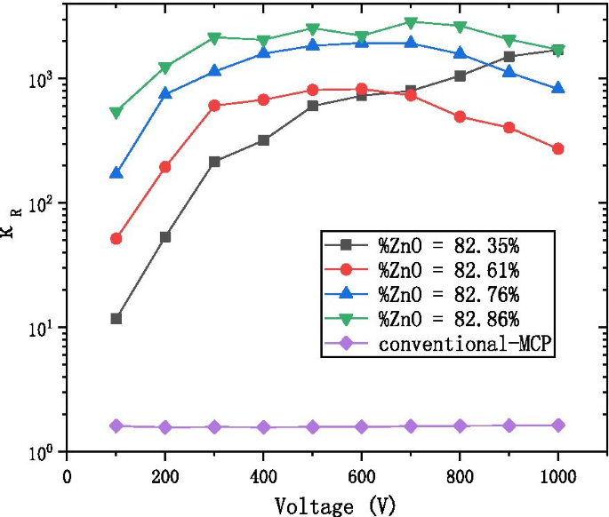
K R 不同AZO-ALD-MCP配比下的电压图
图 9 显示了“相邻”材料设计的电阻与工作电压的比值 \(L_{R}\)。比率 \(L_{R}\) 定义为:
$$L_{R} =\frac{{R\left( {4 + \frac{N - 1}{N}} \right)}}{{R\left( {4 + \frac{N}{N + 1}} \right)}}$$
The resistance of the step length LR with the voltage diagram at the different ratio of the working resistance of neighbor formula
where
$$\left( {\begin{array}{*{20}c} {{\text{ZnO}}} \\ {{\text{Al}}_{2} {\text{O}}_{3} } \\ \end{array} } \right) =\left( {\begin{array}{*{20}c} {4 + \frac{N - 1}{N}} \\ 1 \\ \end{array} } \right) =\left( {\begin{array}{*{20}c} 1 \\ {N - 1} \\ \end{array} } \right)\left[ {\left( {\begin{array}{*{20}c} 4 \\ 1 \\ \end{array} } \right)\left( {\begin{array}{*{20}c} 5 \\ 1 \\ \end{array} } \right)} \right]$$and
$$\left( {\begin{array}{*{20}c} {{\text{ZnO}}} \\ {{\text{Al}}_{2} {\text{O}}_{3} } \\ \end{array} } \right) =\left( {\begin{array}{*{20}c} {4 + \frac{N}{N + 1}} \\ 1 \\ \end{array} } \right) =\left( {\begin{array}{*{20}c} 1 \\ N \\ \end{array} } \right)\left[ {\left( {\begin{array}{*{20}c} 4 \\ 1 \\ \end{array} } \right)\left( {\begin{array}{*{20}c} 5 \\ 1 \\ \end{array} } \right)} \right]$$As can be observed from Fig. 9, the LR value ranges from 2 to 4.5 to adjust ratio of conductive material ZnO and high resistance material \({\text{Al}}_{2} {\text{O}}_{3}\). And it proves the feasibility of WYM operation to design laminated materials.
Figure 10 shows the working resistance with respect to the percentage of ZnO cycles (%ZnO), where %ZnO is defined to be:
$${\text{\% ZnO}} =\frac{{{\text{ZnO}}}}{{{\text{ZnO}} + {\text{Al}}_{2} {\text{O}}_{3} }}{*}100\left( {\text{\% }} \right)$$
The working resistance with the percentage of ZnO cycles diagram at the different voltage
under various voltage conditions, ranging from 100 to 1000 V. It decreases that the working resistance under the same voltage with the increase in the percentage of ZnO cycles. It can be the same that the working resistance under different the percentage of ZnO cycles and under the different condition of voltage. Therefore, the AZO-ALD-MCP of different formulations works under its specific voltage to meet the MCP resistance index.
We define the ratio of the resistance difference under the different condition of voltage and the voltage difference to describe the effect of the voltage on the resistance of MCP:
$$r =\left| {\frac{{R_{U} - R_{V} }}{U - V}} \right| =\left| {\frac{{R_{1000v} - R_{100v} }}{1000 - 100}} \right|$$Figure 11 shows that the effect of the voltage on the resistance of AZO-ALD-MCP decreased and gradually stabilized with the increase in the percentage of ZnO cycles. Therefore, the preparation of AZO-ALD-MCP should try to choose a formula with a large percentage of ZnO cycles.

The r with the percentage of ZnO cycles diagram at the working state
Based on the above analysis, we have put forward the reference to the working resistance for the conductive layer of ALD-MCP. As shown in Fig. 5a, we design the AZO conductive layer of AZO-MCP by using the WYM operation and temperature adjustment based on the working resistance. We use atomic layer deposition technology to grow the \({\text{Al}}_{2} {\text{O}}_{3}\) emission layer on microchannel wall of the two-dimensional pore arrays [3, 11, 22]. In Fig. 12a, the gain from our AZO-ALD-MCP is compared to that of a conventional MCP under different voltages. As can be observed, our preparation method of the AZO-ALD-MCP provides a larger gain than that of a conventional MCP. Figure 12b shows the phosphor screen with uniform green light under high pressure, thus proving the uniformity of the material deposited on the wall of each microchannel and the uniformity of the AZO-ALD-MCP field of view.

The gain with the voltage diagram at the AZO-ALD-MCP and conventional-MCP
结论
We defined the working and non-working resistance of the microchannel plate. Aiming at the required resistivity of the microchannel plate in the region with extremely narrow zinc content requirement (70–73%), an algorithm for growing the AZO conductive layer is proposed. Compared with the conventional MCP, we found a large difference between the working and non-working resistance and there is also a huge difference under different voltages. Therefore, we analyze the data by defining \(\kappa_{R} ,L_{R} ,\% {\text{ZnO}},r\). MCP should try to choose a formula with a large percentage of ZnO cycles. We recommend using the working resistance as an ALD-MCP resistance indicator in industrial production. Building on our results as described in this work, our studies will help to find even better materials as the conductive layer for the ALD-MCP.
Change history
纳米材料