

汽车 PCB 特性和设计注意事项
电子元件在汽车中发挥着越来越积极的作用。目前,一辆顶级汽车包含200多个电子控制单元,其中一些是应用于汽车驾驶舱的传感器和处理器。可以得出结论,为汽车服务的电子产品的价值在于动力系统、车身和底盘,其中大部分与数字电源有关。
电子系统在汽车中的应用旨在提高汽车性能,包括三个方面:
a.环境改善是指节油、减少尾气、燃料由汽油、天然气、生物燃料向混合动力和纯动力转变。因此,电动汽车已成为汽车行业的战略方向。
b.安全增强在于减少交通事故,从安全气囊、雷达监控、立体摄像头、红外监控和自动避让到自动驾驶。目前,自动驾驶汽车正吸引着大多数人的关注和投资。
c.便利和舒适一般植根于音频、视频显示、空调、电脑、移动通讯、互联网、导航和电子收费等方面,出于便利性和人性化的考虑。
作为电子设备的支柱,应用于汽车的PCB(印刷电路板)也必须满足上述要求。
汽车 PCB 的基本要求
• 质量保证要求
对制造商或经销商来说,长期质量保证的一个基本要求在于完善的质量管理体系,即国际视野下的ISO9001。由于汽车行业的特殊性,1994年北美三大汽车制造商共同建立了汽车行业独有的质量管理体系,即QS9000。 21 st 开始 世纪,世界汽车制造商根据ISO9001的规定发布了新的质量管理体系,即ISO/TS16949。
作为全球汽车行业的技术法规,ISO/TS16949整合了汽车行业的特殊要求,专注于汽车零部件供应链的缺陷预防、质量波动和减少浪费。
因此,汽车PCB制造商在真正进入汽车市场之前必须获得的第一个证书是ISO/TS16949。
• 性能基本要求
一个。高可靠性
汽车可靠性主要体现在两个方面:一是控制单元和电子元件正常工作的使用寿命;二是耐环境性,使汽车控制单元和电子元件在极端环境下表现出色。
汽车的平均使用寿命为 10 至 12 年,在此期间只能更换零部件或易损件。换句话说,电子系统和PCB必须像汽车一样具有服务年限。
车辆在应用过程中往往会受到气候和环境的影响,从严寒、酷热到长期暴晒雨淋。除此之外,他们还必须承受由工作电子元件和系统产生的热量导致的环境变化。汽车电子系统和PCB也是如此。汽车电子系统必须克服以下恶劣环境,包括温度、湿度、雨水、酸烟、振动、电磁干扰 (EMI) 和电流浪涌。
湾。轻量化、小型化
轻量化和小型化有利于节省燃料,这得益于每个组件和电路板的轻量化和小型化。例如,车载ECU(Electronic Control Unit)的体积为1200cm 3 在 21 st 的开头 世纪,而这一数字至少缩小了四倍。 PCB的轻量化和小型化源于密度的提高、面积的减小、薄型化和多层化。
汽车 PCB 的性能特性
• 多种类型
作为机械和电子设备的结合,现代汽车技术融合了传统技术和最新科学技术。不同的零件依赖于不同功能的电子设备,导致PCB的应用任务不同。
根据汽车用PCB基板材料的区别,可分为无机陶瓷类PCB和有机树脂类PCB。陶瓷基PCB的主要特性是高耐热性和优异的尺寸稳定性,适用于高热环境下的发动机系统。然而,陶瓷基PCB的可制造性较差,导致电路板成本高。随着新开发的具有更高耐热性的树脂基板的开发,树脂基PCB主要应用于大多数现代汽车。
遵循一个一般规则:使用具有不同性能的基板材料的PCB应用于车辆的不同部分,负责实现不同的功能。下表展示了与部分车载设备或仪器兼容的PCB类型。
| 车载设备 | PCB 类型 |
| 车速表;空调 | 单/双层PCB 单/双层柔性PCB |
| 汽车音响;监控 | 双层PCB 多层PCB 柔性PCB |
| 汽车通讯设备;无线定位设备;安全控制系统 | 多层PCB HDI PCB 柔性PCB |
| 引擎系统;动力传输控制系统 | 金属芯PCB 刚柔结合板 |
| 车载电源控制器;导航装置 | 嵌入式PCB |
• 车辆不同部位PCB的可靠性要求
汽车作为一种涉及公共安全的交通工具,属于高可靠性产品。除了机械和电子方面的一般尺寸、外观和性能要求外,还需要对其进行一系列的可靠性测试。
一个。热循环测试(TCT)
根据车辆的不同部分设置5个级别。下表总结了车辆不同部分 PCB 的热循环温度:
| 车辆部分 | 级别 | 低温 | 高温 |
| 车内 | A | -40°C | 85°C |
| 下面是车辆底盘 | B | -40°C | 125°C |
| 引擎之上 | C | -40°C | 145°C |
| 传动部分 | D | -40°C | 155°C |
| 引擎内 | E | -40°C | 165°C |
湾。热冲击测试(TST)
汽车PCB应用在极端高温环境中是很正常的,这对于重铜PCB来说尤其具有挑战性,因为它们必须同时承受外部热量和自身身体产生的热量。因此,对汽车PCB的耐热性提出了更高的要求。
车用PCB要参加热冲击测试,必须在260°C或288°C的高温焊膏中浸泡10秒3次,合格的PCB没有层压、凸块或铜裂等问题.如今,无铅焊接已用于PCB组装,焊接温度较高,增加了热冲击测试的必要性。
C。温湿度偏差(THB)测试
汽车PCB必须经过包括雨天和潮湿环境在内的众多动态环境,这使得有必要进行THB测试,该测试也能够检查PCB CAF(导电阳极丝)流动性。 CAF只发生在以下几种情况:电路板上相邻的过孔之间、相邻的过孔和导线之间、相邻的导线和相邻的层之间。在这些情况下,绝缘性会降低甚至导致捷径。绝缘电阻应根据过孔、导线和层之间的距离来确定。
汽车PCB的制造特点
• 高频电路板
与军用雷达类似,作为近场雷达,汽车防撞或预测性紧急制动系统依赖于 PCB 传输微波高频信号。因此,建议使用具有低介电损耗的基板材料,通常使用 PTFE(聚四氟乙烯)。与普通的FR-4作为基材不同,PTFE或类似的高频材料自然需要不同的可制造性。例如,在通孔钻孔的过程中需要特殊的钻孔速度。
• 厚铜PCB
由于电子密度和功率高,车辆往往会产生更多的热量。随着混合动力和纯电动汽车数量的增加,需要先进的动力传输系统,这对散热能力和更大的电流提出了更高的要求。为此,应增加PCB中铜的厚度或在多层PCB中嵌入铜引线和金属。
制造厚铜双层PCB很容易,而制造厚铜多层PCB却相当困难。重点在于重铜图形蚀刻和重铜间隙填充。
重铜多层PCB的内部电路是重铜。之后,图形转移需要具有极高耐腐蚀性的厚膜。刻蚀时间要足够长,刻蚀设备和工艺条件要处于最佳状态,才能保证厚铜电路的优良。
由于内导体和绝缘基板材料表面存在巨大差异,普通多层PCB叠层无法使树脂完全填充,导致产生空洞,因此建议使用含有大量树脂的薄预浸料。一些多层PCB包含不同铜厚的内部电路,因此可以在区分大和小的区域使用不同的预浸料。
• 组件嵌入
嵌入式组件 PCB 最初应用于手机,以增加组装密度并减小产品的整体尺寸,这对其他电子产品也很重要。这就是嵌入式技术用于汽车电子设备的原因。
基于组件嵌入方法,有许多嵌入式 PCB 制造选项:
a.首先铣槽,然后通过波峰焊或导电膏组装 SMD。
b.薄膜贴片首先通过波峰焊组装到内部电路上。
c.厚膜元件印刷在陶瓷基板上。
d. SMD通过波峰焊组装,然后使用树脂进行封装。这种嵌入式PCB更符合汽车的耐热、耐湿、抗冲击等需求,可靠性高。
• HDI 技术
与智能手机或平板电脑在娱乐和通讯功能方面类似,车辆也需要HDI PCB。因此,微孔钻孔、电镀和互连技术必须应用于汽车PCB。
汽车 PCB 设计注意事项
• 电感器方向
当两个电感(甚至是两根PCB线)相互靠近时,就会产生电感。一个电路(电路 A)中的电流产生的磁场随后将驱动另一个电路(电路 B)中的电流。这个过程类似于变压器初级和次级项圈之间的相互影响。当两个电流通过磁场相互作用时,产生的电压由互感 (LM) 决定:  。 In this formula, YB is the error voltage input to Circuit B while LA is the current through Circuit A. LM is quite sensitive to circuit spacing, inductance loop area and loop direction.
Therefore, an optimal method to arrange all inductors in a circuit can be achieved through compact circuit layout and coupling balance reduction.
Distribution of mutual inductance is related with inductance alignment. Therefore, direction modification of Circuit B makes its current loop parallel to magnetic lines of Circuit A. To achieve that, inductors should be vertically arranged, which is beneficial to mutual inductance reduction.
Inductor layout rules for automotive PCBs:
a. Inductor space should be as large as possible;
b. Inductor alignment should be set as right angles so that crosstalk between them will be minimized.
• Lead coupling
Similar with inductor alignment affecting magnetic field coupling, if leads are close to each other, coupling will be affected as well and mutual inductance will be possibly generated. The leading issue in RF circuit lies in sensitive component layout such as input matching network, receiver's resonant channel and emitter's antenna matching network.
Return current path should be as close to main current path as possible with radiation field minimized, which is beneficial to current loop area reduction. Optimal low impedance path is normally grounding area under leads, that is, loop area is effectively limited in the area with dielectric thickness times lead length. If grounding area is split, however, loop area will be enlarged. For leads going across split area, return current will be forced to go across high impedance path, which greatly increases current loop area. This type of layout also makes circuit accessible to mutual inductance.
In a word, integrated grounding should be ensured under leads as much as possible since integrated mass area grounding is beneficial to circuit performance improvement.
• Grounding thru-hole
The main issue RF circuit has to solve usually lies in bad characteristic impedance of circuits, including electronic components and interconnection. Copper layer with low thickness is equivalent to inductance wire. Moreover, distributed capacitance can be formed by the combination between copper layer and adjacent leads. As leads go through thru holes, inductance and capacitance characteristics will be displayed as well.
Thru-hole capacitance mainly derives from capacitance between copper at thru-hole pad edge and bottom copper. Another element affecting thru-hole capacitance is cylinder of metal thru holes. Parasitic capacitance affects little since it usually just leads to low signal edge of high-speed digital signals.
The largest effect of thru holes is corresponding parasitic inductance aroused by interconnection. Because majority of metal thru holes feature the same dimension as that of integrated components in RF PCB design, this formula can be used to estimate the effect of thru hole: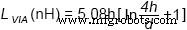 . In this formula, LVIA is the integrated inductance of thru holes; h refers to via height with inch as unit; d refers to via diameter with inch as unit.
As a result, circuit layout should conform to the following principles:
a. Inductance module should be established for thru holes in sensitive area;
b. Filter or matching network depends on independent thru holes;
c. Thinner PCB copper will reduce the effect of thru hole parasitic inductance.
• Grounding and filling
Grounding or power plane defines a public reference voltage that supplies power to all components in the system through low impedance path. Based on that scheme, all the electric fields can be balanced with excellent shielding scheme generated.
Direct current always flows through low impedance path. Similarly, high-frequency current is also a path flowing through the lowest impedance at the first minute. Therefore, for standard PCB leads above ground plane, return current tries to flow into the grounding area rightly under leads. Afterwards, split grounding area arouses all kinds of noises, which further increases crosstalk through magnetic field coupling or current accumulation. As a result, ground integrity should be ensured as much as possible, or return current will drive crosstalk.
In addition, filling ground, also called protective wire, is usually applied for design of circuits containing areas where continuous ground is difficult to be arranged or that requires shielding sensitive circuits. Grounding thru holes can be positioned at terminals of wires or along the wires to increase shielding effect. Protective wires can't be mixed with leads designed to provide return current path, which will bring forward crosstalk.
When copper area isn't connected to ground or connected to ground at one terminal, its validity will be decreased. In some cases, parasitic capacitance will be generated with ambient impedance changed or potential path formed between circuits, which, thus, lead to bad effect. Simply speaking, if copper has to be arranged on the board, the same electroplating thickness should be maintained.
In the end, grounding area near antenna has to be taken into consideration. Any monopole regards grounding area, routing and thru hole as a section of system balance and non-ideal balanced routing will affect radiation efficiency and direction of antenna. Therefore, grounding area mustn't be directly placed right under monopole antenna of a circuit board.
To sum up, the following design principles should be conformed to in terms of grounding and filling:
a. Continuous grounding area with low impedance should be provided as much as possible;
b. Two terminals of filling wires should be connected to the ground with thru hole array applied;
c. Copper-coated lines have to be connected to the ground near circuit around which copper coatings aren't necessary. When it comes to circuit boards with multiple layers, a grounding thru hole should be arranged as signal lines are transferred from one side to the other.
In conclusion, automotive PCB design rules can be summarized into the following table:
| Inductor layout | • Inductor space should be as large as possible; • Inductor alignment should be set as right angles; |
| Integrated grounding | • Integrated grounding should be arranged under leads; |
| Through holes | • Inductance module should be set for thru holes in sensitive area; • Filter or matching network depends on independent thru holes; • Thinner PCB copper reduces the effect of thru hole parasitic inductance; |
| Grounding and filling | • Continuous grounding area with low impedance should be provided; • Connect terminals of filling wires to the ground with thru hole array applied; • Copper-coated lines have to connected to the ground; |
Article wrote by PCBCart editor Dora Yang, first published on Bodo's Power System Magazine August issue, 2017.
You might also be interested in the following articles:
• Properties of Flex-Rigid PCB Used for Automotives
• 5 Tips for Automotive Circuit Design to Defeat EMI
• SMT Soldering Reliability Research Based on Circuit Module in Automotive Electronic Industry
• 5 Proven Ways to Judge Reliability of Automotive PCB Manufacturers
• How to Evaluate an Automotive HDI PCB Manufacturer
工业技术