

揭示金属辅助化学蚀刻过程中多孔硅纳米线的形态演变和蚀刻动力学
摘要
用金属辅助化学蚀刻制造的多孔硅纳米线 (SiNW) 的许多潜在应用高度依赖于对器件优化形态的精确控制。然而,关键蚀刻参数的影响,如沉积金属催化剂的量、HF-氧化剂摩尔比(χ ) 和溶剂浓度对 SiNW 的形态和蚀刻动力学的影响仍未得到充分探索。在这里,系统地研究了具有化学沉积银催化剂的 HF-H2O2-H2O 蚀刻系统中简并掺杂 p 型硅的纳米结构和蚀刻速率的变化。发现表面形态在足够高的 χ 下从微孔和凹坑结构演变为均匀的 SiNW 阵列 值。纳米结构底部和尖端的蚀刻速率分别与由 Ag 引起的初次蚀刻和由金属离子和扩散孔引起的二次蚀刻相关。 H2O 浓度也会影响 χ SiNW 形成的窗口和蚀刻速率,主要是通过调节反应物稀释和扩散速率。通过χ控制二次刻蚀和反应物扩散 和 H2O 浓度,成功地证明了制备具有独立控制孔隙率的高度掺杂的 SiNWs,这有可能用于提高 SiNW 基器件的性能。
背景
尽管在各种新型材料上取得了研究突破,但硅仍然是制造纳米结构最有吸引力的基材之一,因为它在自然界中很丰富,并且存在成熟的器件集成技术。近年来,一维硅纳米结构,如硅纳米线(SiNWs)和纳米柱,在光伏[1, 2]、热电[3, 4]、储能等广泛应用中不断受到关注。 [5,6,7]、柔性电子 [8]、生化传感 [9] 和生物接口 [10]。除了此类纳米结构独特的电学、光学、热学和机械性能外,其持续吸引力的主要驱动力是开发新型制造技术,该技术允许纳米结构的轻松形成,同时保持对形态和物理性能的出色控制。在各种制造技术中,金属辅助化学蚀刻 (MACE) 因其简单、低成本和灵活性而从工业角度脱颖而出 [11, 12]。使用 MACE,只需选择合适的 Si 晶片、蚀刻剂成分、反应温度和反应时间,即可获得具有定义长度、孔隙率、电导率、掺杂水平和晶体取向的晶片级无缺陷 SiNW [13,14, 15、16、17、18、19、20、21、22、23]。 SiNW 直径、横截面和阵列间距的控制也可以通过催化剂图案化技术实现,例如纳米球光刻 [24]、干涉光刻 [25] 和嵌段共聚物光刻 [26]。这与其他制造技术形成对比,例如反应离子蚀刻和汽-液-固方法,这些技术需要昂贵的设备,并且可能生产具有表面缺陷、不受控制的晶体取向和有限横截面形状的纳米线 [11]。
在过去的十年中,使用 MACE 从高掺杂的 Si 晶片制造 SiNW 受到了特别的关注,因为由此产生的多孔 SiNW 具有高结晶质量 [14, 17, 19]。多孔结构使纳米线获得非常理想的特性,例如可调光致发光 [15]、低导热率 [27] 和高比表面积 [28],使它们成为光电子学 [14, 16]、热电学 [ 3, 27],光催化 [28, 29] 和能量存储 [5]。结合它们的光致发光和高表面积,多孔 SiNW 在生理环境中的生物相容性和生物降解性也使其成为生物标记 [15] 和药物递送应用 [30] 的合适候选者。尽管通过在蚀刻剂中使用高浓度的氧化剂可以用低掺杂的 Si 晶片获得相对多孔的 SiNW [15],但在需要高导电性的情况下使用高掺杂的 Si 是有利的,因为它避免了对蚀刻后掺杂的需要步。这在多孔 SiNW 的热电应用中尤其如此,其中品质因数的提高是由于热导率的降低而没有显着降低电导率 [27]。另一方面,据报道,多孔 SiNWs 的电阻与固体 SiNWs 相比相当大 [14],这意味着孔隙度和电导率之间的权衡。
为了实现多孔SiNW在上述应用中的潜力,必须充分了解高掺杂Si的MACE过程中各种蚀刻参数的影响。许多研究 [13,14,15,16,17, 19,20,21, 23] 已经在 HF-H2O2 蚀刻剂中使用 MACE 成功制造了具有不同长度和孔隙率的高掺杂 SiNW。他们的研究揭示了 H2O2 浓度 [14,15,16,17,20,21,23]、HF 浓度 [21]、HF-H2O2 体积比 [19]、蚀刻持续时间 [14,16,17] 的影响, 19,20,21, 23] 和蚀刻温度 [19,20,21, 23] 对孔隙率 [14, 16, 17, 19, 20], 长度 [16, 17, 19,20,21, 23 ]、蚀刻速率 [15] 和 SiNW 阵列的整体形态 [15, 16, 21]。然而,对蚀刻剂 HF-H2O2 摩尔比影响的系统研究,定义为 χ =[HF]/([HF] + [H2O2]),并且H2O浓度对高掺杂Si纳米结构的形成是有限的。尽管 χ 是确定 Si 纳米结构的形态和蚀刻速率的关键参数 [18, 31],而 [H2O] 在微图案区域 [18] 中形成 SiNW 的关键。迄今为止,只有 Chiappini 等人。 [15] 和 Balasundaram 等人。 [19] 使用了广泛的χ 值(分别为 0.4-0.98 和 0.7-0.99)在高掺杂 SiNW 的制造中,而没有人充分探索蚀刻剂 [H2O] 的影响。此外,尽管许多研究阐明了用 MACE [15, 17, 32] 制造的轻掺杂和重掺杂 SiNW 的形态演化、孔隙化和锥形化的机制,但由于沉积金属的竞争效应而导致长度演化的机制蚀刻、再成核金属蚀刻、空穴扩散和反应物扩散尚未得到充分研究。在这项研究中,使用无电沉积的 Ag 催化剂和 H2O2 氧化剂在简并掺杂的 p 型硅晶片上进行了两步 MACE [33]。与使用图案化 Au 催化剂的 MACE 相比,化学沉积只能形成具有不同直径的随机分布的 SiNW [13],而 Ag 可能会限制可实现的 SiNW 纵横比,因为其溶解速度比 Au 快 [11]。尽管如此,在 MACE 中使用化学沉积和银催化剂被认为是形成包括 SiNW 在内的 Si 纳米结构的最简单和最便宜的方法。为了探索蚀刻剂成分对所得纳米结构和蚀刻速率的影响,具有相对较宽范围的 χ 蚀刻剂 和 [H2O] 值被利用。通过确定 Si 纳米结构尖端和底部的蚀刻动力学,深入了解空穴注入和 Si 溶解速率的影响,溶解金属离子和扩散空穴引起的二次蚀刻,以及反应物的扩散速率对所得形态和长度的影响提供了纳米结构。还使用由不同 χ 组成的蚀刻剂制造了相同长度的高掺杂 SiNW [H2O] 和 [H2O] 值,从而表明尽管蚀刻持续时间不同,但可以通过蚀刻剂成分有效地调整孔隙率。
方法
电阻率为 0.001-0.005 Ω cm 的单面抛光硼掺杂 p 型 Si (100) 晶片和抛光面上的 50 nm 热氧化层用作起始材料。用去离子 (DI) 水、丙酮和乙醇彻底清洁晶片,并用稀 HF 去除热氧化物,从而形成 H 端接的 Si 表面。为了将蚀刻限制在抛光的 Si 表面上,Si 晶片的背面涂有光刻胶 (AZ5214)。通过将晶片切割成 1 × 1 cm 2 获得用于 MACE 实验的 Si 样品 件。每组实验均使用来自同一晶片的硅样品。
MACE 使用两步蚀刻工艺进行,包括无电沉积 Ag 催化剂,然后在 HF-H2O2 溶液中蚀刻,如图 1 所示。首先将 Si 片浸入 5% HF 中 3 分钟。然后,在含有 4.8 M HF 和 0.005 M AgNO3 的水溶液中,在 Si 基板上无电沉积 Ag 纳米颗粒 (AgNP),持续不同的时间(图 1a)。用去离子水温和冲洗后,在具有不同 χ 的 HF-H2O2 水溶液中蚀刻 AgNP 包覆的 Si 样品 和 [H2O] 值(参见附加文件 1:表 S1)不同时间长度(图 1b)。蚀刻后的 Si 样品用去离子水彻底冲洗,然后浸入 1:1 (v /v ) HNO3 10 分钟以溶解 AgNP。在另一次彻底的去离子水冲洗后,将硅样品在 5% HF 中浸泡 3 分钟以去除任何形成的氧化层,然后再次用去离子水冲洗多次。 Ag 沉积和 HF-H2O2 蚀刻在黑暗中进行。所有样品均在室温(22-23°C)下在单独的塑料烧杯中处理,其中包含 15 毫升所需溶液。
<图片>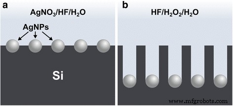
使用两步 MACE 制造 Si 纳米结构的横截面示意图。 一 在第一步中,AgNPs 在含有 AgNO3 和 HF 的水溶液中化学沉积在 Si 表面上。 b 第二步,AgNPs在HF、H2O2和H2O组成的溶液中催化Si衬底蚀刻,形成Si纳米结构
蚀刻的硅表面通过扫描电子显微镜(SEM,Phenom Pro 或 FEI/Philips XL-30)和透射电子显微镜(TEM,Philips CM20)表征。为了准备用于 SEM 观察的样品,背面的光刻胶用丙酮去除。然后用乙醇冲洗硅样品并在电炉上干燥,以最大程度地减少由于水分蒸发引起的硅纳米线团聚[19]。
结果与讨论
银催化剂沉积和多孔 SiNW 的形成
研究了在 0.005 M AgNO3 和 4.8 M HF 溶液中的 Ag 沉积持续时间(10 秒到 15 分钟)对高掺杂 SiNW 形成的影响。当载有 Ag 的样品在含有 4.8 M H2O 和 χ 的溶液中蚀刻时 =0.95 30 分钟,较短的沉积时间(≤2 分钟)导致密集的垂直孔阵列和一些横向凹坑,如图 2a 所示。然而,如果沉积时间≤ 1 分钟,孔的密度不足以形成分离良好的纳米线结构。另一方面,在 4 分钟的 Ag 沉积时间下获得几乎没有缺陷的 SiNW(图 2b),更高的沉积时间导致无凹坑的 SiNW。除了 SiNW 形态的变化之外,还观察到 SiNW 蚀刻速率相对于 Ag 沉积时间的非单调变化,如图 2c(菱形符号)所示。 SiNW 蚀刻速率从 10 秒的沉积时间增加到 4 分钟,但在 4 分钟和 6 分钟之间意外下降。之后,蚀刻速率再次增加,直到 15 分钟,尽管蚀刻速率值相对较低。
<图片>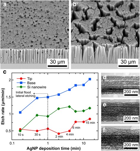
使用包含 0.005 M AgNO3 和 4.8 M HF 的 Ag 沉积溶液以及由 48 M H2O 和 0.95 HF-H2O2 摩尔比组成的蚀刻剂溶液制造 SiNW。对于a的Ag沉积时间,SiNWs的SEM图像 30 s 和 b 4 分钟c 不同 Ag 沉积时间下 SiNW 的蚀刻速率。对于 d 的 Ag 沉积时间,SiNW 中间部分的 TEM 图像 4、e 10 和 f 图15显示了孔隙度。所有样品的蚀刻持续时间为 30 分钟
为了说明 SiNW 蚀刻速率的特殊趋势,还通过将蚀刻的 Si 样品的显微照片与未蚀刻的 Si 的显微照片对齐,从横截面 SEM 图像中确定了 SiNW 尖端和底部的蚀刻速率来自背面同一晶片的样品(参见附加文件 1:图 S1)。从图 2c 可以看出,SiNW 基底(方形符号)处的蚀刻速率随着 AgNP 沉积时间单调增加。另一方面,从SiNW尖端蚀刻速率的趋势线(圆圈符号)可以看出三个域:(a)≤1分钟,蚀刻速率相对较高; (b) 在 1 到 6 分钟之间,蚀刻速率相对较低; (c) ≥6 分钟,此时蚀刻速率最高。因此,SiNW 蚀刻速率从 10 秒的沉积时间到 1 分钟的初始增加是由于基部蚀刻速率的不断增加,而随后在 2 和 4 分钟的沉积时间中蚀刻速率的增加是由于尖端处相对较低的蚀刻速率。同时,沉积时间为 6 min 时 SiNW 蚀刻速率的下降和后续沉积时间中相对较低的蚀刻速率是由于尖端处蚀刻速率的增加所致。
由于 AgNPs 的表面覆盖率与 Ag 沉积时间直接相关 [22, 34, 35],低沉积时间的横向点蚀可归因于稀疏的 Ag 网络 [18, 34, 36] 与一些孤立的 AgNPs 移动随机 <100> 方向由于它们的不规则形状 [37]。由于 Ag 催化剂量的增加,基部的 SiNW 蚀刻速率预计会随着 Ag 沉积时间的增加而增加,这为 H2O2 的空穴注入提供了更多的表面积。此外,更多的 Ag 也意味着更多的 Ag 被 H2O2 氧化 [15, 17],导致更高浓度的 Ag + 离子可以通过电流置换反应促进 Si 溶解 [31]。另一方面,对于 Ag 沉积时间≤1 分钟的尖端处相对较高的蚀刻速率可以解释为由来自稀疏 Ag 网络的不规则形状的 AgNP 引起的初始泛滥横向蚀刻。随后随着Ag沉积时间的增加,尖端蚀刻速率的增加可归因于尖端金属再成核速率的增加[17, 38],以及在较小程度上空穴扩散[31, 39]。
随着 Ag 沉积时间的增加,制造的 SiNW 的孔隙率总体增加,如图 2d-f 所示。 (参见附加文件 1:补充 TEM 图像的图 S2a-c。)由于 Ag + 浓度较高,预计孔隙化会增加 离子,导致重新成核的金属和离子诱导蚀刻 [15, 17, 38]。此外,更高的空穴注入速率也可能导致更多的扩散空穴,这可能有助于孔的形成 [19, 39]。在大多数纳米线中,SiNW 的多孔结构似乎以多孔壳的形式出现,与之前研究中观察到的类似 [14, 17]。对于某些 Ag 沉积时间为 15 分钟的 SiNW,侧壁显得相当粗糙,具有相对较大(约 20 纳米直径)的黑点,这可能是由于再成核的 Ag 颗粒较大。然而,孔隙率分布并不明确:一些 Ag 沉积时间为 4 分钟的 SiNW 的孔隙率与 Ag 沉积时间为 10 分钟的 SiNW 的孔隙率几乎相同;银沉积时间分别为 10 和 15 分钟的 SiNW 也是如此。这可能是由于从样品的不同区域获得的 SiNW,其孔隙化率略有不同,具体取决于沉积(或重新成核)的 AgNP 的实际数量和未反应蚀刻剂的浓度,预计在侧面会更高的样本。尽管如此,这里观察到的总体趋势表明,沉积的 Ag 总量为控制 SiNW 的孔隙率提供了另一个自由度。
孔隙度从 SiNW 的底部到尖端增加(参见附加文件 1:图 S2d-l),类似于之前的研究 [16, 19]。这是由于纳米线的上部区域暴露于蚀刻剂的时间更长而导致的 [19]。另一方面,大多数 SiNW 具有锥形纵向轮廓,这是使用 Ag-MACE 制造的高掺杂 SiNW 的特征,因为 AgNP 在 SiNW 基部连续溶解并在其他位置重新成核 [15, 17 ]。尽管如此,还是有一些 SiNW 具有轻微的双圆锥形或沙漏形轮廓,即中间横截面分别大于或小于顶部和底部横截面。这表明移动 Ag + 离子不仅可以重新沉积到纳米线的上部,还可以重新沉积到底部相邻的 AgNPs 上。
硅纳米结构的蚀刻剂成分和形态演变
使用 χ 确定简并掺杂 Si 中所得纳米结构的形态 0.7 到 0.99 的值和 46、48 和 50 M 的 H2O 浓度。AgNPs 的化学沉积在 0.005 AgNO3 和 4.8 M HF 的溶液中进行 4 分钟,同时在 HF-H2O2-H2O 溶液中进行蚀刻30分钟。图 3 显示了从 SEM 看到的 Si 表面的形态。对于 [H2O] =46 M 和 48 M,蚀刻的 Si 上的特征是从带有陨石坑的微孔 Si 演变而来的(χ =0.7 和 0.75,图 3d,e),到具有深孔的大孔 (χ =0.75 和 0.80,图 3f),然后到 SiNWs (χ ≥ 0.85)。对于 [H2O] =50 M,Si 表面的演变略有不同:与抛光的 Si (χ =0.7), 大孔深孔 (χ =0.75), 到带有陨石坑的微孔硅 (χ =0.8–0.85),然后到 SiNWs (χ ≥ 0.9)。与 Chiappini 等人的工作相反。 [15],多孔硅薄膜顶部的 SiNWs 为 0.7 <χ <0.95 未观察到,并且在更大的 χ 中获得了仅 SiNW 结构 范围 (χ ≥ 0.85 而不是 χ> 0.95)。这些差异很可能是由于沉积的 AgNPs 数量、蚀刻时间、H2O 浓度以及 HNO3 和 HF 蚀刻后处理的变化造成的。
<图片>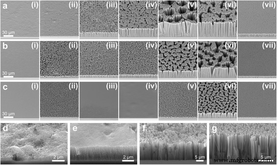
在 H2O 浓度为 a 的溶液中蚀刻的 Si 表面的 SEM 图像 46 M,b 48 M 和 c (i) 的 50 M 和 HF–H2O2 摩尔比 0.7、(ii) 0.75,(iii) 0.8、(iv) 0.85,(v) 0.9、(vi) 0.95 和 (vii) 0.99。 d –g a中样品的高倍SEM图像 (i) , (ii ), (iii ) 和 (vii ), 分别。样品在 HF–H2O2 中蚀刻 30 分钟
获得的 Si 形貌可以用 Ag-Si 界面的电流密度和 Ag + 来解释 离子诱导蚀刻 [15, 17, 31, 38]。高χ下SiNWs的形成 值(≥0.85 或 0.9)可归因于在低电流密度下形成微孔 Si,随后通过抛光溶解微孔 Si [31, 38]。类似的机制很可能是在 χ 下形成具有深孔的大孔 Si 的原因。 值,除了孔端较高的电流密度导致氧化物形成和随后的空穴扩散 [31],导致顶部表面的浅大孔。由于正肖特基势垒高度将注入的空穴从金属-Si 界面拉开 [40],因此预计这种空穴扩散对于高度掺杂的 p 型 Si 尤为重要。也有可能是相对较高的 [H2O2] 与 [HF] 比导致显着的 Ag 溶解,进而导致 Si 衬底中深孔密度低。另一方面,在χ处出现带有陨石坑的微孔Si =0.7–0.85 表示在这个χ中出现低电流密度 范围,这与 Chartier 等人的观察结果一致。 [31] 此外,Ag + 对 Si 的伴随孔隙化 离子也预计会出现在这种情况下。在较高的χ下形成SiNWs 最稀蚀刻剂 (50 M H2O) 的值与 Chiappini 等人的观察结果一致。 [15] 较高的乙醇浓度有利于形成多孔和抛光的 Si 而不是 SiNW。这些结果可能是由于沿 Si 纳米结构深度的低 HF 和 H2O2 浓度梯度导致反应物缓慢扩散到纳米结构基底。在这种情况下,尖端蚀刻的影响变得相对显着,金属颗粒无法形成深孔。
应该注意的是,对于相对较低的 χ 值 (≤0.8),整个 Si 表面的形态不均匀(参见附加文件 1:图 S3)。对于[H2O] =50 M,对于χ也发生不均匀蚀刻 =0.85。在所有情况下,只有在形成 SiNW 时才能获得均匀蚀刻的表面。对于不均匀蚀刻的表面,具有同源形态的部分往往出现在距样品中心大致相同的一般位置。样品不同区域的非均匀蚀刻动力学可以通过溶液中溶解的催化剂离子浓度的增加及其随后扩散到样品其他区域并在其上重新成核来解释。蚀刻Si时H2气泡的同时向外扩散在一定程度上促进了这一点。
在非常高的χ 值 (0.99),获得了非常密集的精细 SiNW 阵列,导致黑色样品表面(参见附加文件 1:图 S3a-c(vii))。然而,许多这些 SiNW 具有倾斜的侧壁和一些横向凹坑,两者都发生在基部附近(图 3g)并且蚀刻时间很长(附加文件 1:图 S4d)。还可以看到许多纳米线形成过早终止的凸起。这些特征可能是由于蚀刻溶液中 H2O2 的耗尽导致 AgNP 膜的各个部分下沉的速度不同造成的。随着银网络的解体,一些银纳米颗粒或小银膜部分开始在水平<100>方向上蚀刻。
MACE 过程中 Si 纳米结构的蚀刻动力学
蚀刻速率随χ的变化 对于不同的 [H2O] 值,如图 4 所示。纳米结构的表观蚀刻速率通常随着 χ 而增加 和 χ 处的峰值 =0.95,之后蚀刻速率显着下降。无论 [H2O] 和 Si 纳米结构的形态如何,这种趋势都是正确的。然而,可以看出 [H2O] 显着影响了蚀刻速率的大小,随着 [H2O] 值的降低(即蚀刻剂浓度更高)而增加。图 4b 显示在 χ 后尖端的蚀刻速率大大降低 =0.85 [H2O] =46 和 48 M 以及 χ 之后 =0.9 [H2O] =50 M。另一方面,图 4c 显示基底处的蚀刻速率在 χ 处显着增加 =0.85 和 0.9,对于 46 M H2O 蚀刻剂,但对于 48 和 50 M H2O 蚀刻剂仅略有下降。基部的蚀刻速率保持在 χ =0.95 但在 χ 处显着下降 =0.99。
<图片>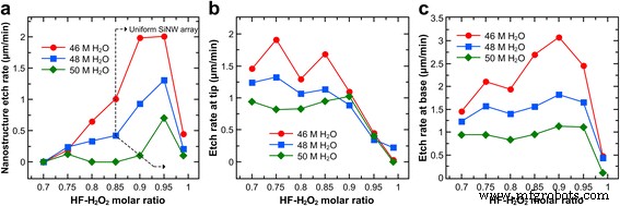
在由不同 HF-H2O2 摩尔比和 H2O 浓度组成的溶液中蚀刻 30 分钟后观察到的表观蚀刻速率。 一 基于所得长度的 Si 纳米结构的蚀刻速率。 b , c 体硅相对于硅纳米结构尖端和基部的刻蚀速率
从Si纳米结构尖端和底部蚀刻速率的趋势可以确定,[H2O] =46 M时SiNW长度的增加主要是由于底部蚀刻的加速,而[H2O] =48 和 50 M 的 SiNW 主要取决于尖端蚀刻的抑制。此外,整体纳米结构蚀刻速率的趋势与基部蚀刻速率的趋势并不完全相同。特别是 χ 基部出现峰值蚀刻速率的值和 χ 由于尖端蚀刻速率的竞争效应,实现最大纳米结构高度的值不同(分别为 0.9 和 0.95)。
χ 出现峰值 SiNW 长度的值 (0.95) 接近 Qi 等人获得的值。 [21] (χ =0.91) 对于高度掺杂的 n 型 Si 衬底。 χ 附近发生尖端蚀刻速率的初始下降 =0.85 与观察到的 Si 表面形态演化一致,其中低空穴扩散和 Ag 再成核允许在 χ 处形成 SiNW ≥ 0.85。在 χ 附近,尖端蚀刻速率几乎同时下降和基础蚀刻速率跃升 =0.85 表示空穴和Ag + 先前在较低的 χ 处从蚀刻前沿扩散的离子 由于抑制了 Ag-Si 界面处的氧化物形成,因此值现在被限制在底部。同时,在较高的 χ 增加 [HF] 值加速了 Si 溶解,导致 Ag 渗透率增加。因为对于给定的 χ,当 [H2O] 增加时,[HF] 和 [H2O2] 都会减少 值(参见附加文件 1:表 S1),预计较高 [H2O] 值时尖端和底部的蚀刻速率会降低。 χ之间的基础蚀刻速率增加较小 =0.85 和 0.95(对于 [H2O]) =48 和 50 M 是由于反应物通过 SiNW 长度扩散较慢,蚀刻剂更稀。
在 χ =0.9,由于 H2O2 空穴注入和 HF 溶解 Si 的最佳速率,基底处的蚀刻速率最大。低于此值,[HF] 是决定速率的因素,因为氧化硅的溶解速度不够快;高于此值,[H2O2] 决定了反应速率,因为注入的空穴数量太少。溶液中 H2O2 的消耗解释了为什么基部的蚀刻速率在 χ 处开始下降 =0.95 并在 χ 处急剧下降 =0.99。蚀刻速率对 [HF] 和 [H2O2] 的这种依赖性先前已观察到 [21],这意味着在 Si 的 MACE 反应速率的任何表达式中都应考虑两种反应物浓度。另一方面,χ 的最大值 从尖端蚀刻速率看不明显。相反,尖端蚀刻速率主要由 [H2O2] 决定。由于 Si 纳米结构尖端的蚀刻主要归因于金属离子再成核和空穴扩散,因此这种相关性是合理的,因为相对于 [HF] 的 [H2O2] 值越高,移动的 Ag + 浓度越高 离子 [15, 17] 和注入空穴 [31, 32]。
不同蚀刻剂成分的 SiNW 长度随时间的演变
SiNW 的长度是光伏 [2]、能量存储 [6]、传感 [41] 和热电应用 [4] 中的一个重要参数。为了制造指定长度的 SiNW,用 χ 确定了蚀刻剂的 SiNW 长度的时间变化 =0.9、0.92、0.95 和 0.98 和 [H2O] =46、48 和 50 M。对于这些实验,AgNP 沉积时间增加到 10 分钟,以最大限度地减少使用长蚀刻时间制造的 SiNW 中的横向点蚀(参见附加文件 1:图 S4a-c)。同样,最高的χ 使用的值为 0.98,因为对于 χ 获得了具有倾斜侧壁和横向凹坑的 SiNW =0.99,即使 AgNP 沉积时间为 10 分钟(参见附加文件 1:图 S4d)。
图 5a 显示形成的 SiNW 的长度随着 MACE 反应时间的增加而增加,这与之前研究中的观察结果一致 [14、16、17、18、19、21、23]。然而,可以看出 SiNW 长度的增加随着时间的推移而减少,即蚀刻速率正在降低(参见附加文件 1:图 S5a),这可能是由于 SiNW 尖端处的蚀刻速率增加或在基地或两者兼而有之。图 5d 显示了 χ 的尖端蚀刻速率随时间增加 =0.92 和 0.95,前者的增加更为明显(参见附加文件 1:图 S5b)。这表明 SiNW 尖端处再成核的 Ag 量增加,预计对于较低的 χ 更显着 值。另一方面,图 5e 显示在蚀刻时间大于 5 分钟时,SiNW 基底处的蚀刻速率对于 χ 几乎是恒定的 =0.9 和 0.92 但随着 χ 下降 =0.95 和 0.98(参见附加文件 1:图 S5c)。后者可能是由于较长的扩散长度导致反应物扩散到 SiNW 基体受阻(SiNW 长度对于 χ =0.95 和 0.98) 并消耗蚀刻液中的 H2O2。
<图片>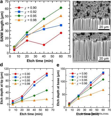
在 48 M H2O 下,不同 HF-H2O2 摩尔比的 SiNW 长度随时间的演变。 一 Effect of etch time on SiNW length. b , c SEM images of SiNWs after etching for 1 h in a solution composed of 48 M H2O and HF–H2O2 molar ratios of 0.9 and 0.98, respectively. d , e Etched bulk Si thickness with respect to the tip and base of the SiNWs over time
It should be noted from Fig. 5 that at χ = 0.9, the evolution of length with time is erratic because of the non-monotonic trend of the etch rate at the tip (see Additional file 1:Figure S5b). This may be due to differing amounts of re-nucleated Ag as more mobile Ag + ions were generated. Nevertheless, lower χ values have the advantage of forming defect-free SiNWs (Fig. 5b) as higher χ may result in some lateral pits, as shown in Fig. 5c for χ = 0.98. The trend of the overall etch rates and etch rates at the tip and base of the SiNWs with respect to χ mirrors those observed in Fig. 4. However, it can be seen in Fig. 5e that χ = 0.92, which is not included in Fig. 4, actually results in a higher base etch rate than χ = 0.9.
The SiNW length also increases with etch duration for more concentrated (46 M H2O) and dilute (50 M H2O) etchants, as shown in Fig. 6a. Likewise, the etch rate decreases with etch time for all H2O concentrations used (see Additional file 1:Figure S6a). Figure 5d, e show that, while the etch depth at the tip and base of the SiNWs both increase with time, the amount of increase at the tip is almost constant but that at the base is decreasing (see Additional file 1:Figure S6b, c). These trends are consistent with those observed for χ = 0.95 in Fig. 5 and Additional file 1:Figure S5. Hence, for χ = 0.95, the increase in the amount of re-nucleated Ag at the SiNW tips with time is negligible, while the increasing SiNW lengths progressively hampers reactant diffusion to the SiNW base. Figure 6 also shows that regardless of the etching time point, lower [H2O] generally results in more etched Si, similar to what was observed in Fig. 4. However, Fig. 6b, c show that low [H2O] solutions may result in some lateral pitting in the SiNWs whereas high [H2O] solutions do not. This could be due to fast etching at sites with re-nucleated Ag particles for low [H2O] etchants.

Evolution of SiNW length with time for different H2O concentrations at a fixed HF–H2O2 molar ratio of 0.95. 一 Effect of etch time on SiNW length. b , c SEM images of SiNWs after etching for 1 h in a solution composed of HF–H2O2 molar ratios of 0.95 and H2O concentrations of 46 and 50 M, respectively. d , e Etched bulk Si thickness with respect to the tip and base of the SiNWs over time
Fabrication of Highly Doped SiNWs with Controlled Porosity
SiNW porosity is another key parameter in SiNW-based devices [5, 16, 27, 29], making its controlled formation during SiNW fabrication highly important. The degree of porosity of SiNWs fabricated using two-step MACE is directly related to the H2O2 concentration [14,15,16,17, 20], etching time [14, 16, 17, 20], and temperature [20] and inversely related to the HF–H2O2 volume ratio [19] and wafer resistivity [17]. In our Ag deposition experiment, SiNW porosity was also found to be directly related to the amount of deposited Ag. However, the extent of SiNW porosification cannot be easily tuned without affecting other parameters. For example, length and porosity are expected to vary together if one of them is adjusted using either [H2O2], etch time, or temperature. If a SiNW of a specific length needs to have higher porosity, the [H2O2] can be increased, but the etch duration needs to be decreased as higher [H2O2] may have a higher etch rate. This raises the question of whether the desired porosity can still be achieved given the shorter etch time.
Here, the extent of SiNW porosification caused independently by χ and [H2O] was compared for χ = 0.92, 0.95, and 0.98 ([H2O] fixed at 48 M) and [H2O] = 46, 48, and 50 M (χ fixed at 0.95). The SiNW length was fixed at 20 μm by using different etch durations based on the etch rate of the respective etchant composition (see Additional file 1:Table S2). The porosity, in general, was found to be inversely related to χ and directly related to [H2O], as shown in Fig. 7a–c and Fig. 7d, b, e, respectively. (The trends are more apparent in Additional file 1:Figure S7 where more samples are shown.) Comparing the SiNWs for χ = 0.95 and χ = 0.98 (Fig. 7b, c), the samples for χ = 0.95 appear to have a higher pore density and most are surrounded by a thin porous shell [14, 17]. Meanwhile, for χ = 0.98, some SiNWs appear to be rough and solid rather than porous, which indicates a much lesser degree of porosification. On the other hand, the overall porosity obtained for χ = 0.92 (Fig. 7a and Additional file 1:Figure S7a) appears to depart from the expected trend. While some SiNWs have a porous shell, others seem to be only roughened although to a higher extent compared with those for χ = 0.98. In contrast, the increase of porosity with [H2O] is more consistent. Although no rough solid SiNWs were obtained for [H2O] = 46 M, highly porous SiNWs were formed for [H2O] = 50 M unlike in the case of χ = 0.92.

TEM images of fabricated SiNWs with a length of ≈20 μm showing the variation of porosity at the middle section with a –c HF–H2O2 molar ratio and d , b , c H2O concentration. 一 –c HF–H2O2 molar ratio of the etchant was 0.92, 0.95, and 0.98, respectively, with [H2O] = 48 M. d , b , c H2O concentration of the etchant was 46, 48, and 50 M, respectively, with HF–H2O2 molar ratio = 0.95. TEM images of SiNWs with f –h low and i –k high porosity corresponding to those shown in c 和 e , respectively, but including the f , i top and h , k bottom sections. The scale bar in e and k also applies to the images in a –d 和 f –j , 分别
The higher SiNW porosity obtained for χ = 0.95 than χ = 0.98 is consistent with the fact that metal re-nucleation, metal ion-induced etching, and hole diffusion are higher for lower χ 值。 It also shows that the longer etch time utilized for χ = 0.98 to obtain 20-μm long SiNWs did not overcome the porosification caused by the etchant χ value. The seemingly lesser degree of porosification for χ = 0.92 could not have been due to the difference in etch time as a longer etching period was utilized for it than for χ = 0.95. It is possible that more porous SiNWs were actually obtained for χ = 0.92; however, due to the very high porosity, HF–H2O2 etching of porous Si both at the surface and inside the pore walls resulted, leading to the rapid collapse of the porous shells [42] and subsequent exposure of the less porous Si surface underneath. That more porous SiNWs were obtained for higher [H2O] values confirms that etch duration has a significant effect on porosity [14, 16, 17, 20]. (Note the large differences in etch times in Additional file 1:Table S2 for different [H2O] values.) The high degree of porosity obtained for 50 M H2O without the collapse of the porous shell could be due to minimized HF–H2O2 etching inside the pore walls because of the lower diffusion rate of reactants in dilute etchants.
Examination of the surface roughness along the length of the SiNWs reveals the characteristic increase in porosity from the base to the tip of highly doped SiNWs fabricated with MACE [16, 19], as shown in Fig. 7f–k (also in Additional file 1:Figure S8). The increase in porosity towards the tip of the SiNWs is due to the longer exposure time of these portions in the etchant solution [19]. Figure 6f–k and Additional file 1:Figure S8 also show that the SiNWs are tapered, with the tapering being more severe in SiNWs which are more porous (Fig. 7i–k and Additional file 1:Figure S8a–c). This is expected considering that porosification is directly related to the amount of dissolution of the metal catalyst at the SiNW base [15, 17]. However, a closer look at the SiNWs reveals that some nanowires exhibit a slightly biconic or hourglass longitudinal profile, which seems to occur more often among those with higher porosity. Likewise, more porous SiNWs generally have larger diameters than the less porous ones (see Additional file 1:Figure S7). In order to achieve highly porous SiNWs with smaller diameters, it might be necessary to use a more inert catalyst like Au [32].
Based on the results obtained here, porosity control in highly doped SiNWs of a given length is possible through the use of the appropriate etchant composition. To achieve low porosity, it is best to use high χ values as rough solid nanowires could be obtained. To achieve highly porous SiNWs, on the other hand, the use of dilute etchants with moderate χ values (≈0.95) is advisable as this avoids the disintegration of the porous shell which occurs in etchants with low χ 值。 It is conceivable that lower porosities could be achieved using an etchant of both high χ and low [H2O] values and higher porosities using an etchant of both (slightly) lower χ and high [H2O] values. In the case of low-porosity SiNWs, the maximum χ and minimum [H2O] values would probably be dictated by the values where considerable lateral pitting occurs. On the other hand, for high-porosity SiNWs, the minimum χ and maximum [H2O] values would be determined by the values where the porous shell dissolves and the SiNW structures are lost, respectively. These methods can be combined with our earlier finding of porosity control via the amount deposited Ag in order to obtain a wide range of SiNW porosities.
Conclusions
Porous SiNWs were fabricated from degenerately doped p-type Si substrates using metal-assisted chemical etching in HF–H2O2 with electrolessly deposited Ag catalyst. The effect of Ag deposition time, etchant HF–H2O2 molar ratio, and etchant H2O concentration on the morphology and etch rate of the Si nanostructures was systematically studied. It was shown that there is an optimal amount of deposited Ag particles necessary to form damage-free SiNWs. Furthermore, the amount of deposited Ag particles affects the SiNW etch rate in a non-monotonic manner and provides an additional mechanism to control the porosity of the resulting nanowires. Likewise, the etchant composition has a significant effect on the resulting nanostructures. There is an appropriate χ window within which uniform SiNW arrays can be formed. For H2O concentrations between 46 and 48 M, this χ range is 0.85–0.98; more dilute etchants increase the minimum χ due to sluggish etching at the SiNW base. The formation of Si nanostructures during Ag-catalyzed chemical etching is a result of the competing effects of different factors, namely, deposited Ag-catalyzed Si dissolution, re-nucleated Ag-catalyzed Si dissolution, hole diffusion, and reactant diffusion through etched pores, as reflected by the etching kinetics at the tip and base of the Si nanostructures. These factors result in a gradually decreasing etch rate over time, with re-nucleated Ag-catalyzed etching being dominant for low χ values and impeded diffusion being more pronounced for high χ 值。 These mechanisms can be exploited to control the porosity of SiNWs of the same length fabricated with different etch times. In particular, suppressing Ag re-nucleation and hole diffusion using higher χ values can effectively decrease pore density, while more controlled porosification can be achieved using dilute etchants owing to slower reactant diffusion and longer etch times. Since the general mechanism of Ag- and Au-catalyzed MACE of Si is similar [11, 33, 35], the findings of this study may also apply to porous SiNWs fabricated with Au metal catalyst, except that metal ion-induced etching is expected to be greatly suppressed and hole diffusion acts as the main mechanism of porosification and tip etching.
缩写
- AgNP:
-
Ag nanoparticle
- DI:
-
Deionized
- MACE:
-
Metal-assisted chemical etching
- SEM:
-
Scanning electron microscopy
- SiNW:
-
Silicon nanowire
- TEM:
-
透射电子显微镜
- χ :
-
HF–oxidant molar ratio
纳米材料