

迈向智能多材料纤维的数字化制造
摘要
纤维无处不在,而且通常是被动的。在光纤中实现的光电子技术可以彻底改变多个应用领域,包括生物合成和可穿戴电子产品、环境传感和能量收集。然而,在纤维中实现高性能电子器件仍然是一项艰巨的挑战,因为材料加工策略难以捉摸,该策略允许将晶体半导体(如硅)制成的器件以有序、可寻址、和可扩展的方式。当前的光纤传感器制造方法要么是不可扩展的,要么将半导体的选择限制为非晶半导体,例如硫属化物玻璃,其电子性能不如硅,导致与标准硅相比,此类传感器的带宽和灵敏度有限光电二极管。我们的团队证实了类似于超大规模集成 (VLSI) 的逻辑电路和传感系统的通用光纤制造,这使得现代微处理器的出现成为可能。我们开发了一种通用的混合制造方法,可以组装典型的纤维内材料架构,用于集成二氧化硅、硅和高温金属中的微电子设备和系统。这种被称为“用于纤维的 VLSI”或“VLSI-Fi”的方法结合了预制件的 3D 打印、纤维的热拉拔以及通过材料选择性空间相干毛细管分解的纤维嵌入集成设备的拉拔后组装的纤芯。我们相信,这种方法将提供一种新型的耐用、低成本、普遍的纤维设备和传感器,使织物与人造物品(如家具和服装)相结合,并融入物联网 (IoT)。此外,它将推动 3D 打印的创新,将数字制造方法扩展到纳米电子领域。
介绍
尽管玻璃拉制光纤的历史可以追溯到罗马时代,但第一批功能性光纤是在 1792 年由法国 Chappe 兄弟制造的,用于通信目的 [1]。 1842 年,瑞士物理学家让-丹尼尔·科拉登 (Jean-Daniel Colladon) 表明,光可以通过水射流在内部进行引导 [2]。这两项发现催生了数十年的光学和材料工程改进,催生了当今的高效光纤,使世界各地数公里的高速电信和数据存储成为可能,例如完成了 25,000 公里长的跨太平洋海底电缆 (TPC) 1996 年 [3, 4]。此外,光纤传感器 (FOS) 被广泛用于生物医学、石油和天然气、海洋、建筑、化学和航空航天应用 [5, 6]。
使用 Philip Russel 于 1996 年开发的光子晶体光纤 (PCF) 控制和改进光传播的性能为研究更复杂的光纤内部功能结构打开了大门 [7,8,9]。新的微结构也欢迎在其构成中整合材料的多样性 [10, 11] 以设计用于电子学 [12]、光电子学 [11]、纤维内合成 [13]、微流体 [14]、微机电系统 [15, 16] 和生物合成界面 [17]。智能光纤与传统光纤的不同之处在于,它包含了光通信之外的非传统功能以及光纤在商业织物中的典型用途。智能纤维可用于电子纺织品中的美学设计,通过控制纤维因微观结构中的光学干涉而产生的颜色外观 [18] 或用于提高性能,例如在允许光导的传统光纤导管和电介质镜衬的情况下通过空气 [19, 20]。
为了使纤维具有功能性,它应该由具有不同电子特性的材料组成,它的结构应该专门设计来执行给定的功能,并且它的内部特征应该在纳米级减少,比当前电信的核心小几个数量级纤维。光纤通常由光纤制造方法制成,即从称为“预制件”的宏观圆柱形或长方体棒热拉制而成。制造过程从选择合适的纤芯和包层材料开始,例如金属、绝缘体和半导体。例如,第一种包含金属-绝缘体-半导体结构的光纤是在 2004 年开发的,用于光电检测 [21]。选择用于预制件的材料,使其粘度 μ , 在拉制温度下相当,大致下降在 4
预制件本质上是纤维的放大版本,可以使用多种技术构建,例如像地毯一样滚动材料片、像拼图一样堆叠铣削部件或 3D 打印,如图 1a 所示(I) 并在此综述中讨论,然后通过真空烧结进行固结。然后将预制件在炉中加热并拉长成类似焦糖或太妃糖的纤维(参见图 1a (II) 中的拉丝锥),同时根据结构的给定热机械特性(例如粘度、界面)保留其横截面排列能量、相互粘附和不同的热膨胀(图 1a(III))[22]。对于 3D 打印预制件的情况,此过程示意性地显示在图 1a 中。典型的拉伸可以产生数公里的纤维,其横截面直径非常细,纳米级约为 5 nm [23, 24]。
<图片>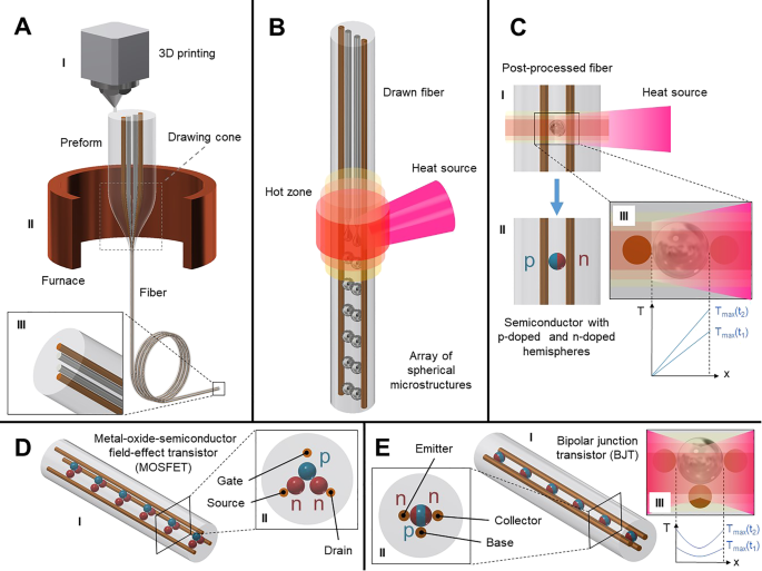
VLSI-Fi:代表“2D + 1D + 0D”方法的 VLSI-Fi 技术的概念示意图。一个 3D 打印的瓶坯 a (I) 被热拉 a (II) 成细长的纤维,保留预制件 (2D) 的横截面几何形状。 b 通过空间连贯、材料选择性毛细管破裂 (+1D) 轴向图案化纤维,导致最初连续、分离的核心组装成并联接触的离散装置阵列。 c 分离驱动的分裂后半导体粒子掺杂控制,允许控制单个器件的内部结构 c (II) 通过热梯度c (三)。 d (I) 通过 VLSI-Fi 的金属氧化物半导体场效应晶体管 (MOSFET) 示意图,其中 p 型和 n 型半导体分别以蓝色和红色显示。嵌入二氧化硅纤维中的金色连续棒充当栅极、源极和漏极。所得纤维横截面显示在 d 中 (二)。同样,e (I) 显示了由 VLSI-Fi 实现的双极结型晶体管 (BJT) 的示意图,通过从发射极和集电极侧同时撞击热源来实现。纤维截面e (II)显示了BJT(嵌入光纤中的连续棒)的发射极、集电极和基极,蓝色和红色分别显示了n-p-n结的p型和n型半导体
在拉伸后的步骤中,利用毛细管不稳定性,可以通过加热使纤维重新液化,以允许以空间连贯的材料选择性方式分解纤芯,从而能够对纤维嵌入结构进行轴向控制 [25,26, 27]如图1b所示。轴向图案化核心的替代技术包括通过光聚合核心中的光掩模进行紫外线曝光,从而产生非平凡形状的微粒 [28]。其他混合功能化技术包括用功能材料涂覆纤维表面 [10, 29] 和通过拉伸 [12] 将纤维包层限制到由标准互补金属氧化物半导体 (CMOS) 制造制造的光电器件阵列。
纤维可以编织成织物或网,以获得超越单根纤维的集体功能[30]。通过仿生学设计,纤维可以根据大自然的有用特征进行塑造,以增强织物的功能,例如疏水性 [31]。纤维也可以被认为是廉价材料生产的合成平台,例如将铝芯转化为二氧化硅包覆纤维中的硅 [13] 或通过相分离热诱导制造多孔结构 [32]。光纤还可以用于远程和分布式信号检测,例如危险挥发物的环境化学传感 [29]。纤维设计的灵活性使得多种功能模式可以集成到一根纤维中,用于复杂的应用,例如深度脊髓皮质刺激和小鼠神经退行性疾病研究的监测 [33]。这些例子展示了智能纤维是自然解决方案的一些领域。
动机
尽管光纤无处不在,但在细光纤中集成高性能微电子系统仍然是一项重大挑战 [11, 12]。已经提出了解决这一挑战的不同方法,主要集中在低温材料上。例如,高压化学气相沉积 (HPCVD) 已被用于在微结构光纤 (MOF) 中集成化合物半导体 [34],以及创建柔性硅 p-i-n 结光纤 [35]。或者,使用 CO2 激光器对石英纤维中的 SiGe 芯进行重结晶,以设计它们的电子特性 [36]。这种方法要么导致器件的电子带宽有限,如硫属化物材料,其本质上是非晶态或本质上是不可缩放的。
因此,纤维和增材制造支持系统实验室 (FAMES Lab) 已经开发并目前实施了一种用于控制纤维 3D 架构的技术,本评论中对此进行了描述。由于最终光纤的复杂性与预制件横截面的复杂性相关,预制件的自由形状制造使光纤设备功能无法实现。此外,3D 打印的应用范围很广,使其成为传统方法的一种经济高效且用户友好的技术替代方案,允许使用范围广泛的材料,从热塑性塑料到高温材料,以及生物材料 [37]。
此外,FAMES 实验室有能力处理高温材料,以及在增材制造中使用更传统的热塑性塑料,使我们能够利用 Si/Ge 中的高电子迁移率等特性 [38],以及作为未来将锆钛酸铅 (PZT)/BaTiO3 复合材料用于压电应用,与聚合物相比具有更大的压电系数 [39, 40] 和更高的声带宽 [41]。
考虑到这些挑战,我们提出了使用增材制造的优化解决方案,以实现更快、更复杂的预制件制造,毛细管破裂模拟以优化纤维的轴向控制,以及我们的纤维与组织工程的组合。这些策略有助于创建具有生物传感和生物功能化能力的现实生物医学平台,用于体外药物和治疗分析,是有前景的光纤器件应用之一。
概念
为了实现功能性纤维,我们从超大规模集成 (VLSI) 中汲取灵感——这种数字设计和制造技术在 1970 年代催生了现代微处理器。该技术使用光刻和化学/热处理半导体衬底晶片的暴露区域来定义该层 (2D) 中集成电路的特征,同时通过在垂直于晶片表面 (+1D)。此外,电路中各个组件的电子掺杂 (+0D) 可以通过注入和热激活来控制 [42]。我们对纤维的处理方法,被称为“用于纤维的 VLSI”或“VLSI-Fi”,与此类似:首先,预制件的增材制造和热拉伸定义了纤维装置 (2D) 的横截面几何形状;其次,所得到的光纤稍后可以进行轴向图案化(+1D),从而允许从最初连续但分离的纤芯组装集成分立器件阵列;第三,可以执行单独的光纤嵌入设备 (0D) 的隔离驱动结构化。表 1 对两种技术进行了比较,突出了每种技术(“2D + 1D + 0D”)实现的几何控制的每个程度之间的对应关系。所描述的步骤的示意图在图 1 中详细显示,其中可能的光纤嵌入设备的示例可以使用 VLSI-Fi 技术实现。
实验部分
在本节中,我们首先描述了我们在聚碳酸酯预制件 3D 打印方面的工作,然后介绍了使用立体光刻技术在玻璃 3D 打印方面的最新进展。然后,我们通过空间连贯的、材料选择性的毛细管破裂来处理纤维的轴向图案,这允许将最初连续的、单独的核心组装成平行接触的离散设备阵列。最后,我们建议应用我们的生物界面纤维,结合组织工程来监测体外活组织的生长。通过使用纤维内微流体通道传递细胞和信号生化物质,使用形状记忆合金线进行运动控制,以及使用压电元件通过超声波绘制环境来实现功能。
3D 打印瓶坯绘图
如前所述,传统的预制件制造技术,如薄膜轧制和堆叠和原始 [10],在生产复杂的几何结构方面受到限制,在光纤拉制过程中占用大量时间,并且需要熟练的技术劳动力和昂贵的设备。 3D 打印借助可溶性支撑材料及其部分自动化和用户友好的过程解决了这些问题。这允许在相对较短的时间内轻松打印非常复杂的几何形状。
为了评估聚碳酸酯 (Hatchbox 3D) 预制件的打印角度的影响,使用单头 Prusa i3 MK2 FDM 打印机打印圆柱形和方形杆。挤出机和打印床的温度分别设置为 235 °C 和 105 °C,并且打印机设置为使用 0.35 毫米喷嘴生产 100% 填充预制件。预制件中各层的取向取决于部件相对于打印床的水平取向,并且当在热拉拔过程中将预制件引入熔炉时,热流受层取向的影响。为了测试哪种方向最适合热拉伸,打印了 0°、15°、30°、45° 和 90° 方向的预制件。所有角度都是在预制件的纵轴和水平轴之间测量的。 3D 打印的预制件在具有 90 °C、100 °C 和 200 °C 三个温度区的熔炉中进行热拉伸过程。对于圆柱形预制件,热拉拔在 0° 和 45° 的角度是成功的。 90°瓶坯拉拔总是因分层而失败。
我们还能够成功绘制非平衡结构,例如具有临时填充图案的方形杆,如图 2a (I) 所示,其中填充图案不是直线填充图案,而是设置为跟随周边并打印在有序的结构中。基于 0° 方形的预制件拉制成功,虽然它略微变形,但光纤仍然能够保持预制件的形状。尺寸低至 40 μm × 60 μm 的纤维被成功拉伸,如图 2a 所示,没有分层。此外,所有层都得到了适当的合并。纤维横截面的示例如图 2a (IV) 所示,退火前后的纤维图像分别如图 2a (V) 和 2a (VI) 所示,其中我们看到退火纤维实现了光学透明度,这将在未来的工作中进行表征。从这些实验中,我们得出结论,最成功的预制件是在 0° 打印的预制件,而 90° 在拉伸过程中总是分层。随着3D打印预制件取向角的减小,热拉伸纤维中的层固结得到改善。
<图片>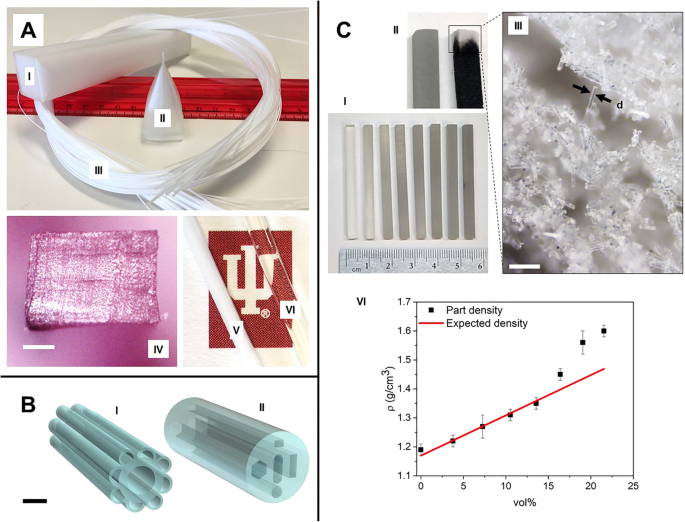
3D 打印瓶坯:a (I) 方形底座 3D 打印聚碳酸酯预制件。 一 (II) 拉锥。 一 (III) 热拉伸后得到的聚碳酸酯纤维。 一 (IV) 拉伸后的纤维截面,无分层。由于填充图案的非各向同性孔隙度(比例尺 200 μm),横截面为矩形。 一 (V) 退火前的拉伸纤维。 一 (VI) 退火后具有明显光学透明性的拉伸纤维。 b 玻璃瓶坯的 CAD 模型,通过基于高精度挤压的 3D 打印在钠钙玻璃中成功实现。 b (I) 结构模仿蓝色狼蛛毛发。 b (II) 具有非平衡截面几何形状的瓶坯模型(比例尺 1 cm)。 c (I) 使用 SLA 技术打印的玻璃填充量不断增加的方形玻璃样品(从左到右)。 c (II) 玻璃样品在烘烤前(左)和烘烤过程中(右)的细节。在后者中,可以看到树脂碳化残留物导致的黑色,而这些残留物灰化后尖端呈现白色。 c (III) 灰化部分显微镜下的图片(比例尺 200 μm),其中白色是相互连接的多孔结构中压实的研磨纤维的自然颜色的结果。此外,玻璃纤维的标称宽度(在图像中由 d 表示)与预期值 16 μm(#38 Fiber Glast)相关。 c (IV) 打印的玻璃瓶坯密度图 (ρ ) 作为与树脂混合的玻璃纤维的体积分数以及打印材料的平均密度的函数
玻璃瓶坯的 3D 打印
除了热塑性塑料,包括熔融石英在内的玻璃在光学、通信和电子领域具有重要的科学和工程应用 [43]。结构化二氧化硅光纤可以使多种应用受益,例如用于时尚的织物的无染料着色、用于光化学检测的光子晶体光纤或用于电信和光的紧密聚焦的单模光纤。这些光纤通常通过 2 个步骤制造:预制件制造和将预制件热拉制成光纤。虽然拉丝工艺相对简单且便宜,但此时的瓶坯制造需要逐案处理,并且对于每个特定的瓶坯配置,必须开发和应用单独的技术。
图 2b 显示了钠钙玻璃预制件计算机辅助设计 (CAD) 模型,该模型在基于挤压的打印技术中以高精度成功实现,类似于 Micron3DP 公司描述的产品 [44]。这种材料具有良好的光学特性,尤其是在长波长(如 IR)[45] 中,使其成为制造具有新型光学功能的光纤的有趣候选材料。图 2b (I) 中所示的预制件模型模仿了蓝色狼蛛毛发的结构,类似于 [46] 中提出的结构,在图 2b (II) 中,预制件横截面包含非平衡几何形状,并且是因此由于表面张力最小化而易于重塑。这些模型的设计和实现是为了验证实现复杂的非平衡预制件横截面的可能性。
由于包层结构在拉制过程中为光纤提供了机械完整性——由最粘稠的材料组成——我们迄今为止的努力一直集中在光纤的这个组件上,我们最终的目标是保持横截面几何形状的预制件。从长远来看,我们的目标是开发多材料挤出技术,这将使我们能够将多种材料整体集成到同一张印刷品中。或者,可以用粉末材料(例如 Si 或 Ge)填充该结构。然后可以烧结填充的结构以获得预成型件。古门尼克等人。已经描述了类似的方法[47]。
如果有兴趣生产以钠钙玻璃为芯材的纤维,一种简单的方法是打印悬浮芯预制棒。悬芯光纤在各种应用中受到关注,包括传感 [48] 和低损耗太赫兹引导 [49],并且通常用聚合物实现 [49]。在这种类型的光纤几何结构中,纤芯由将其连接到外层的支柱支撑。绘制后,这些结构被缩小到感兴趣的波长数量级的尺寸,对于引导光,效果是悬浮的核心。门罗等人。已经报道了各种材料(如二氧化硅和铋玻璃)中的悬浮芯纤维 [48]。他们还提供了一系列这些纤维传感应用的例子,特别是在生物和化学传感方面,证实了这些纤维几何结构的可行性。
已经使用光固化二氧化硅纳米复合材料设计了使用定制树脂进行基于立体光刻的玻璃 3D 打印的新方法 [50]。在这里,我们提出了一种基于现成的商用树脂通过 3D 打印制造玻璃纤维预制件的方法,使其成为使用立体光刻 (SLA) 实现 3D 打印玻璃部件的一种经济高效且更简单的方法。 SLA 打印机(Formlabs 的 Form 2)使用波长为 405 nm 的激光进行操作,随着构建的平台逐层上升,树脂通过桶底部交联。
为了获得玻璃印刷品,我们使用商业透明树脂 (Formlabs FLGPCL04 Clear) 和 0.79 mm (1/32") 硼硅玻璃纤维(#38 Fiber Glast)的混合物进行印刷。这可以很好地控制最终打印材料的组成和实现纤维所需性能的灵活性。使用磁力搅拌器将玻璃纤维分散到透明树脂中。玻璃以小增量添加,每次添加后均质约 3 分钟。对于打印过程,打印机设置为开放模式以允许使用我们的定制树脂。尺寸为 4 × 4 × 50 mm 的长方体预制件以 90° 方向打印。打印后,将部件浸入异丙醇中 10 分钟以去除多余的树脂, 并在 60 °C 下用紫外线灯后固化 30 分钟。随着玻璃纤维与印刷树脂混合的体积比增加(从左到右),固化玻璃预制件如图 2c (I) 所示。
然后对预成型件进行后处理,以去除残留树脂并烧结玻璃颗粒,从而形成完全由玻璃组成的部件。这些工艺对预制件的影响如图 2c (II) 所示,其中我们看到了固化后(左)和烘烤工艺后(右)的预制件。在后者中,可以看到在灰化炉中烘烤产生的黑色,而在脱脂后尖端呈现白色。图 2c (III) 显示了烧结前预制件在显微镜下拍摄的图像,其中可以看到所有树脂确实从零件中烘焙出来,导致仅由玻璃纤维形成的互连结构。必须控制几个参数,例如烘烤温度和加热曲线,以控制化学反应和收缩。使用灰化炉实现粘合剂的热脱脂。得到的棕色部件在高温管式炉中烧结。在1300 °C的温度和5 × 10 -2 的压力下进行烧结 mbar,遵循 [51] 中规定的协议。将保持阶段设定为 800 °C,以蒸发分子结合的水和表面结合的硅烷醇基团。真空烧结提高了光学透明度,因为它减少了烧结玻璃部件内部的空气[52]。
在后处理之后,测量零件的体积和重量以获得密度。然后将其与由可固化树脂和玻璃纤维混合物组成的打印材料的平均密度进行比较,计算公式为 ρ avg =ρ 树脂 (1 − χ v) + ρ 玻璃 (χ v),其中 ρ 树脂 =1.17 g/cm 3 是固化透明树脂的密度,ρ 玻璃 =2.55 g/cm 3 是磨碎的玻璃纤维的密度,χ v为混入树脂中的玻璃纤维的体积比。
结果显示在表 2 和图 2c (IV) 中,其中我们展示了树脂中不同体积比例的玻璃纤维的打印部件密度,与打印材料的平均密度相比。我们观察到,对于混合到树脂中的较低玻璃体积比,获得的结果在预期范围内。然而,在较高的玻璃浓度下,我们看到了与理想密度的线性行为的偏差。这可以归因于打印过程中的沉淀,在这些体积比下变得显着,从而有效地在这些打印中产生更高浓度的玻璃。印刷过程发生在罐的底部,在印刷过程中,由于沉淀,玻璃浓度不断增加。它从(及以上)应落在计算曲线上的初始均匀浓度开始。
从表 2 中可以看出,在 21.54 vol% 研磨玻璃纤维填充部分,实测密度为 1.61 g/cm 3 ,即实际体积比例为 31.88 vol%。在实验过程中,我们得到了一个实际填充有 34.78 vol% 研磨玻璃纤维的样品。这一结果与 Kotz 等人制造的 37.5 vol% 二氧化硅填充物相去甚远。 [53],与我们在这项工作中使用的商业树脂相比,开发了一种定制树脂。这项工作的未来方向包括热处理程序、零件烧结以及所得零件的机械和光学性能的研究。
掺杂的相干材料选择性毛细管破裂和分离控制
一旦预制件被热拉伸,结果是一种长而细的纤维,其中保留了横截面,如图 1a (III) 所示。对于具有一个或多个纤芯的光纤,这些纤芯可以通过空间相干、材料选择性毛细管破裂过程 [26] 轴向图案化,如图 3 所示。而 Tomotika 模型探索了周期性不稳定性的形成无限、均匀加热的流体圆柱体,考虑到周围流体的影响 [55],传播瑞利不稳定性引入了前传播的概念 [56]。尽管在文献中可以找到毛细管不稳定性数学处理的几个例子,例如 Liang 等人。 [57],这些工作主要集中在等温方案上,这在我们的案例中不适用。此外,我们的案例具有传播热梯度和粘度梯度的额外复杂性。因此,它可能更接近于边缘不稳定性标准驱动的过程,如 Powers 等人所述。 [56]。通过结合计算和实验结果,我们旨在通过轴向热梯度现象建立纤维断裂的数学模型。
<图片>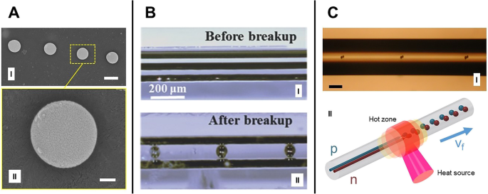
毛细管破裂:a (I) 纤维截面显示通过毛细管破裂形成的 Si 球体(比例尺 0.5 μm)。 一 (II) 描述形状质量的单球体图像(比例尺 100 nm),来自 Gumennik 等人。 [26]。 b (I) b之前单根石英光纤中的金属-半导体-金属光电探测装置示例 (I) 和 b 之后 (II) 分手过程,来自 Wei 等人。 [54]。 c (I) 将双芯光纤分解为双球形簇(比例尺 100 μm),来自 Gumennik 等人。 [26]。 c (二)c所示过程示意图 (I),p型和n型核分别用蓝色和红色表示
毛细管破裂模拟的现阶段侧重于静止状态。我们有兴趣分析在受到热梯度影响的初始静止光纤中如何首先发展不稳定性。这个过程类似于 Gumennik 等人进行的毛细管破裂实验的初始步骤。 [26],其中具有 4 μm 厚 Si 芯的二氧化硅纤维以分别为 0.3 和 0.1 L/min 的流量通过氢氧火焰的热区。虽然这种炬管的最高温度可达2800 °C,但纤维所承受的最高温度必须低于二氧化硅沸点2230 °C。
Considering that the flame width is between 3 and 3.5 mm and that the fiber has a diameter of about 300 μm, it is easy to understand why it is not feasible to experimentally measure the temperature gradient to which the fiber is exposed. Furthermore, the dynamic nature of the breakup process and the fact that it involves multiple materials with varying emissivities further adds to the complexity of the problem, while the fiber’s high aspect ratio and sharp viscosity ratios render the numerical simulation of the full Navier-Stokes equations computationally challenging.
In our simulations (using COMSOL Multiphysics® 5.3a, with its Microfluidics and Heat Transfer modules) shown in Fig. 4a, we assume an axisymmetric fiber with radius r fiber = 140 μm, composed of a thin Silicon core (r core = 2 μm) enclosed in a Silica cladding. Initial heat-transfer simulations showed that a fiber length of 15 mm is sufficient to ensure that the fiber extremities remain at room temperature, thus avoiding influence from the boundaries to the breakup process. Through the sweep of different parameters such as heat source length and distance to the fiber surface, as well as power, we can observe the changes produced in the breakup behavior, thus collecting information about the temperature gradient. Also of importance are the breakup period and speed, parameters which can be compared to experimental results and used for the refinement of the simulations.

Capillary breakup simulations:a Image of the simulated Si core during the first droplet formation, right before the pinch-off for T max = 1900 °C. Color scale represents surface velocity (scale bar = 50 μm). b Snapshot of fiber breakup experiment recording just after the first droplet pinch-off, indicating a breakup time of 14 ± 3 s (scale bar = 60 μm). c Breakup time t breakup for different values of T 最大限度。 The exponential dependence of t breakup on T max is evident, a behavior that is expected due to the dependence of t breakup on the core’s viscosity, which in turn depends exponentially on the temperature. The shaded rectangle encompasses the temperature range compatible with this breakup time-scale. d Si core and SiO2 cladding viscosities as a function of axial position, with temperature pro le over-imposed, for T max = 1900 °C
The simulations are performed in two steps:first, the steady-state temperature profile is calculated for different heat source powers, in order to achieve the desired maximum temperature T 最大限度。 The results are then exported to a time-dependent fluid-flow simulation, where the Navier-Stokes equation is solved with time steps of 0.05 s, from 0 s until the first droplet pinch-off (t breakup), which is dependent on T max, as can be seen in Fig. 4c, where t breakup is plotted for different values of T 最大限度。 It is possible to observe that t breakup has an exponential dependence on T max, which is expected since t breakup is proportional to the core’s viscosity, which in turn is exponentially dependent on the temperature.
The relevant parameters used in these simulations are listed in Table 3. Preliminary simulations indicate that the phase transition of the Si core has no significant influence on the steady-state temperature pro le obtained, neither on the subsequent fluid-flow simulations since, in the entire region where the capillary instabilities occur, the temperature is higher than the melting point of Si. Therefore, in order to maintain the model as less computationally intensive, we simulate a core of liquid Si as a first approximation. Moreover, although a fully coupled heat-transfer and fluid-flow simulation is preferable, we consider that the effects of coupling bring second-order corrections to the solution and thus can be neglected at this stage. An image of the simulated core during the first droplet formation, right before the pinch-off, is shown in Fig. 4a, for T max = 1900 °C. A plot of the densities of silica and silicon, as a function of the axial position (in the simulation, the z-axis) for this particular simulation, is presented in Fig. 4d, with the temperature profile over-imposed.
Our results allow us to define the ranges of viscosities for which the time scales for breakup are comparable to those observed experimentally, thus assessing qualitatively the temperature profile imposed on the fiber. Fig. 4b shows a snapshot of a fiber breakup experiment recording just after the first droplet pinch-off, at the frame corresponding to t = 39 s. Since the resolution of the images before this frame is not ideal, judging on the basis of the symmetry of the breakup behavior, it is possible to assess that the pinch-off of the first droplet occurs at t = 35 ± 3 s, which translates to a breakup time after the temperature steady-state regime is achieved, of 14 ± 3 s. The shaded rectangle in Fig. 4c encompasses the temperature range compatible with this breakup time-scale, from which we can infer that the maximum temperature to which the fiber is exposed is 1885 ± 15 °C. With the collection of statistics on the breakup behavior in the future, we aim to develop a procedure for the temperature measurement of the process, which is otherwise unattainable by conventional means [26, 58, 59].
Moreover, segregation-driven control of doping in post-breakup semiconducting particles is attainable, allowing to control an individual device’s internal architecture. It is possible to control the structure of a single sphere, as was demonstrated by Gumennik et al. [47] shown in Fig. 5. When the droplet is exiting the flame, it experiences a thermal gradient:it is colder on the end distant from the flame, and consequently, it is expected to solidify laterally, starting from the colder side. If the sphere is doped with a material that is more soluble in a liquid than in a solid, this dopant will be repelled into the liquid as the solidi cation front propagates, collecting predominantly on the hot side. This effect is shown schematically in Fig. 1c and can be used to synthesize structured particles, composed for example of Ge-rich Si, (as shown in Fig. 5):Starting with 50:50 Si-Ge mixture in the fiber core, after the breakup the sphere will solidify, such that the Ge is extruded into the melt as the solidi cation evolves, leading to anisotropic distribution and resulting in axially oriented Janus particle heterojunctions [47]. This method can be extremely useful in assembling complex fiber-embedded devices such as heterojunctions, as shown in Fig. 1d and e.

Segregation control of doping:a (I) Schematic illustration of the segregation-driven control of doping in post-breakup semiconducting particles. Details:cross section of a Ge-rich Silicon continuous core in silica fiber a (II) and post-breakup schematic drawing of doping-segregated sphere, or Janus particle, with the Ge-rich side indicated in green a (III). b (I) Scanning Electron Microscope image in backscattered mode of the fiber, polished along its axis, showing an array of Janus particles. b (II) Detail of single Janus particle cross section. b (III) Energy-dispersive X-ray spectroscopy (EDS) map of Janus particle, indicating non-homogeneous distribution of Ge along the cross section, from overlaid maps of Si (in red) and Ge (in green). b (IV) Si-Ge equilibrium phase diagram, liquidus (solid line), and solidus (dashed line). b (V) SiGe atomic content distribution along the dashed line in b (III). (From Gumennik et al. [47])
Biomedical Application
Fiber technology is frequently utilized in various biomedical applications as chemical, biological, and physical sensors. Fiber-embedded sensors have been designed to monitor physical parameters such as stresses, temperature, pressure, and humidity or chemical parameters such as pH level, oxygen concentrations, and carbon dioxide concentrations [60]. Fiber bundles are beneficial to embed multiple sensors together in a single system and in increasing signal reception levels, resulting in higher signal-to-noise ratios. Lightness, flexibility, and unique optical properties are the main characteristics that lead the demand for fiber sensors in biomedical studies. To meet clinical usage requirements, preforms must be fabricated from biocompatible, non-toxic, and chemically inert materials to prevent immune reaction from the patient. Examples of smart fiber development include a neural fiber probe composed of a polymer and metal core composition that enables flexibility and bending stiffness of the neural probe as it provides in vivo optogenetic stimulation and delivers drugs as an input in order to record feedback electrical and physiological output signals [33]. Another example is a fiber integrating microfluidic principles with complex cross-sectional geometries and meter-long microchannels which analyzes cell separation by dielectrophoresis (DEP). Live and dead cells are separated by inertial and dielectrophoretic forces by sheathless, high-throughput microfluidic cell separator which contains conductive materials in the microchannels [14]. The following strategies show a new array of possibilities where smart fibers can be used in biological interfacing.
Consider an artificial gut that can serve as a bioactivity testing platform at the microscale and at the macroscale. With today’s progress in tissue engineering, a variety of functionalities can be integrated in bioink-coated fibers co-extruded using a bioprinter for tissue fabrication, as shown in Fig. 6(I). Traditionally, bioprinting research aims at creating tissue grafts for regenerative medical practice and does so by carefully designing the hydrogel (Fig. 6(II)) with the appropriate nutrition and signaling molecules for the type of cells required based on the application (Fig. 6(III)). Tissue engineering is very challenging to study as the whole biology of the system completely changes microseconds after the experiment has been launched. Monitoring and regularly tuning a tissue’s maturation remains very complex.

Biological interfacing. (I) Three-dimensional bioprinting of a tissue. (II) Standard microextrusion of bioink. (III) Conventional bioink with cells suspended in hydrogel. (IV) Novel coaxial microextrusion of biointerfacing fiber coated in bioink. (V) Close-up view of fiber where biointerfacing occurs:epithelial cells and vascular epithelial growth factors are excreted from different microchannels and result in cellular self-assembled vasculature between two orifices; piezoelectric elements measure surrounding cell density by ultrasound; and shape memory alloy wires provide peristaltic motion in the tissue. (VI) Visualization of biointerfacing fiber and its components
We propose here a solution by introducing smart fibers in the design (Fig. 6(IV)) to provide a better understanding of the climate and environmental growth. The embedded fiber holds multiple functionalities (Fig. 6(VI)) such as inducing vasculogenesis, ultrasonic imaging, peristaltic movement, and microfluidic flow. Control of the microenvironment takes place via the fiber hooked to syringe pumps and wired to an analytical software. The features of this application (Fig. 6(V)), including pilot experimental data, are detailed in the next subsections.
The Extracellular Matrix and Vasculature
Tissue engineering is widely explored with the increase of artificial tissue needs [61, 62], and the ability to bioprint realistic tissue has an important role to play in tomorrow’s drug and treatment development [63, 64]. One of the biggest challenges is the design of the extracellular matrix (ECM), composed of proteins, growth factors, and other biomolecules, that guide the cell’s contribution to the tissue [65]. Naturally, the ECM gives purpose and structure to the cells, and its extraction typically works by decellularizing tissue and recycling or reusing the ECM for a new cellular construct. The ECM comes in the form of solvents, hydrogels, biopolymers, bioceramics, aerogels, or foams to provide biodegradable or resorbable structure to the tissue [66]. Due to tissue engineering’s high complexity in defining the specifics of the biosystem—mechanical properties, scaffold dissolvability or absorption rates, initial cell types, nutrition, density and ratios, growth factors introduction, and its resulting bioactivity and tissue self-assembly—it is vital to assess the behavior of different types of naturally produced ECM or artificially developed biomaterials in the presence of interacting cells. Moreover, viable tissue requires an organized vascular system that supplies nutrition and oxygen to the tissue for the health and growth of cells. Vascularization provides the natural microfluidic feed of biochemicals to initiate proliferation, specialization, interactions, and motion. The vascular network is formed by vasculogenesis, arteriogenesis, and angiogenesis. Vasculogenesis develops its network through the differentiation and division of endothelial stem cell [67]. Angiogenesis forms new sprouts from existing vessels that are formed in the early embryonic vasculogenesis stage [68].
In-Fiber Microfluidic Feed
Microfluidic conduits with periodic microchannels for content delivery can be used to weave microfluids to specific locations in tissue constructs. The liquefaction front at the boundary of the hot zone defines the droplets’ pinch-off location as described previously. Multiple cores can therefore be broken up in a spatially coherent manner. For example, a silica fiber including a platinum and a silicon core can become a fiber tube with multiple outlets, by inducing the silicon core into an array of spheres and then thinning the fiber using hydrogen fluoride, etching the silicon spheres with potassium hydroxide and etching the platinum core with regal water. An example of the result is shown in Fig. 6(V). The flexibility of fibers allows the microfluidic feed to be integrated in multiple ways in tissue construct. In Fig. 6(IV), the microfluidic channels are used to provide the necessary cell type and growth factors to initiate vascularization and angiogenesis as the tissue reaches maturity.
Biomaterial and Biochemical Testing
In parallel to fiber development, a new testing platform (Fig. 7a (I)) was designed to analyze vascularization and cell-to-cell interactions in the presence of growth factors (Fig. 7a (II)). The platforms were printed in high resolution at an orientation of 30 from biocompatible resin by stereolithography (Formlabs’ Form 2 and Dental LT Clear resin). The print result, shown in Fig. 7a (III), was assembled with two glass capillary tubes with outer diameters of 1.8 mm and 1.0 mm where biological agents are fed. Initial trials will assess diffusion parameters of biochemicals and the growth of cellular colonies in various biocompatible materials. These platforms are designed to be single-use. In 2 h, 24 testing wells can be printed at a relatively low cost. The distance between each capillary outlet of two parallel fibers can be adjusted between 100 and 400 m to investigate the optimum vasculogenesis range that is accepted around 200 m [67]. The medium of interaction in the well’s chamber will first host commercial bioinks (Cellink, USA), one containing sodium alginate and nanofibrillar cellulose and the other containing gelatin methacryloyl, before developing our own in-house biomaterials. The glass capillary tubes shown in Fig. 7a (I) will eventually be replaced by the microfluidic fiber shown in Fig. 6a (V) which will be discussed in the next section.

Pilot experiments for biointerfacing:a (I) Cross section of biotesting well showing fluidic feed. 一 (II) Example of the interaction of epithelial cells (blue circles on the left) with vascular endothelial growth factors (yellow dots on the right) resulting in vasculogenesis excreted by the cells (red lines in the center). 一 (III) Printed testing platform in biocompatible resin (scale bar = 5 mm). b Temperature-stress-strain graph of the shape memory effect. c (I) Cross section of in-fiber SMA wires (scale bar = 1 mm). c (II) Side view of in-fiber SMA wires (scale bar = 1 mm). c (III) 5.2-mm segment of an in-fiber SMA wire in contraction after being heated at 80 °C. c (IV) 5.36-mm segment of extended in-fiber SMA wire at room temperature
Peristaltic Motion
Shape memory alloy (SMA) wires are lightweight, non-corrosive, and cost-efficient actuating materials for refined applications in a variety of applications such as prosthetic biomimicry [69], self-expandable surgical implants [70], and aerospace engineering [71].
SMAs are metal compounds known for their shape memory effect and pseudoelasticity. Although such properties are typically found in nickel-titanium, these properties can be found in a range of different other metal alloys. Figure 7(b) shows the shape memory effect in terms of temperature, stress, and strain. As shown, at low temperatures, the SMA in its martensite solid state can be deformed by mechanical force, and when thermally induced, goes through a non-diffusive molecular reordering, converting to an austenite solid state. When cooled, the material will return to its initial martensite form, hence the shape memory effect. This thermal cycle is defined by four temperatures, the starting and finishing martensite and austenite temperatures (M s, M f, A s, and A f), which specifies the start and end of transition periods between states. When the SMA is deformed in as martensite, the molecular de-ordering is defined as detwinning, and it allows the material to experience elongation, which is particularly useful for actuation applications. Essentially, the shape memory effect cycle can occur hundreds of times for an average elongation of 6% and contraction [72], hence its nickname “muscle wire” for its close similarity to muscular myofibrils.
This unique characteristic was first reported by Alden Greninger and Victor Mooradian in 1938 [73], can also be triggered by magnetic field energy [74], namely ferromagnetic shape memory alloys (FSMA), and can be found in polymers (SMP) as well [75]. Today, SMA’s mechanical fatigue and fracture, elasticity, and thermodynamics have been characterized well experimentally [76] and mathematically [77], and its behavior has been modeled [78].
Although the shape memory effect allows for nice contraction behavior of a material, for appropriate robotic applications, the motion needs to be reversable. Typically, an SMA is set in tandem with an opposite mechanism, such as springs, electric drives, elastic bands, or simply another SMA wire. Furthermore, the assembly changes whether it is a linear or rotatory actuation and if the opposing contractions of the actuation are equal. Although wires are thin and weak alone, they can be bundled together to reach the desired force and keep its shape memory effect response time. SMA wires can also be coiled around a capstan to provide greater elongation over shorter distances. Various strategies have been reviewed and chosen for specific applications [79]. The thermal induction is typically best controlled by powering the SMA wire and varying the input current of the order of hundreds of milliamperes. Cooling can be done naturally or by including heat sinks and ventilation.
Fiber drawing technology allows us to play on different material characteristics and to provide to an SMA wire an elastic coating that helps preserve the disorder state of the SMA fiber. As shown in Fig. 7c (I) and c (II), a fiber can be drawn with multiple embedded SMA wires. Styrene-ethylene-butylene-styrene (SEBS) was chosen as the surrounding structure to the SMA wires. SEBS is a copolymer elastomer that can withstand the drawing temperature of 80 °C. While preliminary results show that the actuation can work but with lower efficiency than bare SMA wires, the back-and-forth motion through heating (Fig. 7c (III)) and cooling (Fig. 7c (IV)) cycles is observed for a deformation of approximately 3.07%. More research is required to optimize the setup, but this early stage of experimentation in-fiber SMA actuation shows promising outlooks. The wires were physically pulled and heated using a hot plate to prove the concept. Heating by current would allow speeding up the shape memory effect and controlling better the heat’s diffusion through the fiber. The 5.35-mm wire was measured to have a diameter of 0.11 mm and a resistance of 18.2 was recorded across the fiber segment. To provide a frame of reference, according to SMA wire manufacturers (Dynalloy, Inc.), a 0.1-mm-thick wire made of nickel and titanium requires approximately 200 mA of current for a 1 s contraction. Controlling each wire individually would allow for directional movement, and adding more SMA wires to the design would allow multi-directional motion and greater contraction strength. Moreover, if ferromagnetic SMA wires were used, the control of the motion could become locally controllable via tuning of the interacting magnetic field. Additionally, the FAMES Lab’s drawing tower having the ability to rotate a preform as it is drawing into a fiber enables the possibility to manufacture spring-like structures of SMA wires in the fiber which allows for greater deformation, similar to commercially available SMA springs. Clearly, varieties of strategies are enabled with in-fiber SMA wires.
Biosensing
Biosensors are developed in a wide variety of ways. They can be designed label-based or label-free to detect specific expressions from biological elements such as cells, bacteria, hormones, proteins, DNA, and more [80, 81], from sampling blood, urine, saliva, sweat, or tears. Psychophysiological conditions can be observed from real-time biofeedback such as blood pressure, electrodermal activity, skin conductance, respiration and heart rates, and more [82, 83]. Bioimaging has been done by optical imaging, ultrasound, magnetic resonance frequency, computed tomography, near-infrared spectroscopy, quantum dot probing, and by many more techniques [84].
In optical fiber research, previous biosensing fibers have been fabricated relying on silicon photonic crystal detection of biological radiation [85]. Photonic crystal technology has been used before to monitor in label-free real-time cellular morphology and survival [86]. Such progress in biophotonics has led to hollow-core microstructured fibers visible under magnetic resonance imaging (MRI) [87]. The hollow core allows the propagation of the optical radiations along the fiber over very long distances. The geometry of the hollow fibers varies to tune the photonic bandgaps and dispersion of different detected wavelengths. The inner walls of these hollow tubes are coated with oppositely charged polyelectrolytes and magnetite nanoparticles which are used as contrast agents for MRI. Such design therefore enables new biomedical precision diagnosis opportunities, for example, in the observations of neural activity in vivo [87, 88].
Ultrasonography technology enables us to observe density of cells in liquid or gel in a non-intrusive manner [89, 90]. Ultrasonic probes typically function according to the piezoelectric effect (generation of electricity from applied stress), which was first discovered by Jacques and Pierre Curie in 1880 [91]. The inverse piezoelectric effect (deformation of a piezoelectric crystal from an applied electric field) was induced mathematically by Gabriel Lippmann in 1881 [92] and later in 1916, Chilowsky Constantin and Paul Langevin developed ultrasonic submarine detection for World War I military applications [93]. Thereon, sonar applications have been diverse, such as underwater imaging and fish-finding [94, 95] and energy harvesting [96, 97].
The piezoelectric elements convert electrical energy to and from mechanical energy and transmit sound waves between each other. All frequency and bandwidth parameters require precise regulation, and good energy transmission requires good acoustic and damping matching impedances. Two fibers with integrated piezoelectric elements, designed as pulsing emitter and receiver, can create an ultrasonic waveguide between each other to measure density over the wave’s trajectory. This fiber enables us to sense the microstructures of the environment as the tissue reaches maturation. The piezoelectric elements are created by capillary breakup from a PZT core for example. PZT elements have an acoustic impedance of 33.7 × 10 6 kg/m 2 s with a resonance frequency below 25 MHz. The produced spheres are lined with conductive electrodes to a transducer. This setup provides the feedback in a control system to better adjust microfluidic and motion feed. The in-fiber ultrasonic imaging of the microenvironment clearly helps understand how the tissue environment behaves over time.
结论
We have formulated the concept of VLSI for fibers (VLSI-Fi)—a combination of liquid-phase processing techniques in microelectronic materials forming a toolbox for fabrication of high-performance devices and systems in fibers and textiles. Our experimental work focuses on a set of demonstrations substantiating our control over narrower aspects of VLSI-Fi, such as preform 3D printing, in-fiber circuit assembly by material-selective spatially coherent capillary instability, and segregation-driven doping control at the level of an individual fiber-embedded device. We envision that VLSI-Fi will enable realization of product in multiple technological areas, one of which is fabrication of active biomimetic scaffolds for engineered tissues with realistic microstructures.
数据和材料的可用性
Not applicable.
缩写
- BJT:
-
Bipolar junction transistor
- CAD:
-
Computer-aided design
- CMOS:
-
互补金属氧化物半导体
- DEP:
-
Dielectrophoresis
- ECM:
-
Extracellular matrix
- EDS:
-
能量色散X射线光谱
- FAMES Lab:
-
Fibers and Additive Manufacturing Enabled Systems Laboratory
- FOS:
-
Fiber optic sensors
- FSMA:
-
Ferromagnetic shape memory alloys
- HPCVD:
-
High-pressure chemical vapor deposition
- IoT:
-
Internet of Things
- MOF:
-
Microstructured optical fibers
- MOSFET:
-
Metal-oxide-semiconductor field-effect transistor
- MRI:
-
磁共振成像
- PCF:
-
Photonic crystal fiber
- PZT:
-
Lead zirconate titanate
- SEBS:
-
Styrene-ethylene-butylene-styrene
- SLA:
-
Stereolithography
- SMA:
-
Shape memory alloy
- SMP:
-
Shape memory polymers
- TPC:
-
Trans-Pacific undersea cable
- 紫外线:
-
紫外线
- VLSI:
-
Very large-scale integration
- VLSI-Fi:
-
Very large-scale integration for fibers
纳米材料