

通过纳米压痕加工引起的次表面缺陷对材料位错演化和机械性能的影响
摘要
次表面缺陷对纳米结构的精度和性能有显着影响。本文通过纳米压痕的分子动力学模拟研究了加工引起的次表面缺陷对材料位错演化和力学性能的影响,其中通过符合实际的纳米切削构建了具有次表面缺陷的试样模型。讨论了次表面缺陷的形成机制以及机械诱导缺陷与位错演化的相互作用机制。计算了单晶铜试样的硬度和杨氏弹性模量。仿真结果表明,工件表面下存在稳定的缺陷结构残留物,如原子团、堆垛层错四面体、阶梯位错等。纳米压痕二次加工可以修复工件内部缺陷,但会加剧二次加工区域的亚表面损伤。试样的纳米压痕硬度随着次表面缺陷的引入而增加,从而形成加工硬化效应。次表面缺陷的存在会削弱材料抵抗弹性变形的能力,其中位错与次表面缺陷的相互演化起着重要作用。
背景
纳米尺度的超精密制造被广泛认为是获得具有亚微米尺寸精度和纳米级表面质量的纳米组件的有效方法[1]。制造后,工件内部会留下一些稳定的亚表面缺陷 [2,3,4,5]。亚表面缺陷不仅影响加工精度和表面质量,而且严重影响纳米部件的机械性能和使用寿命。许多关于次表面缺陷的研究已经通过分子动力学(MD)方法进行,主要集中在次表面缺陷s的形成和演化[6, 7],次表面缺陷(SSD)层的厚度[8, 9],以及表面缺陷对表面完整性的影响 [10, 11]。然而,次表面缺陷对工件材料力学性能的影响研究较少。纳米结构的机械性能对其使用性能和寿命至关重要。因此,次表面缺陷对材料力学性能的影响成为研究的关键问题。
许多研究已经通过纳米切割过程的分子动力学模拟来考虑SSD层。 Narayanan [12] 研究了单晶金层错四面体 (SFT) 的形成,并介绍了 SFT 的变形诱导机制。 Inamura [13] 探讨了纳米切削过程中切屑形成和材料滑移变形,并指出切屑形成主要是由剪切滑移变形引起的。裴[14]研究了纳米切削过程中切削参数对位错演化和切削力的影响,发现当工件大于40 nm时,尺寸效应不显着。 Dai[15]和Liu[16]分别采用MD模拟和实验方法研究金刚石工具结构和尺寸效应对工件次表面缺陷演化的影响。以往的研究表明,纳米切割后的工件存在稳定的亚表面缺陷。切削参数和刀具几何参数对次表面损伤层的厚度和演化,甚至加工精度有很大影响。然而,工件材料的力学性能不能通过分析纳米切割获得的相关数据来计算。
纳米压痕是表征硬度和弹性模量等机械性能的有效技术[17]。已经进行了大量关于纳米压痕的研究,以通过实验和理论模型来评估机械性能的性能。 Zimmerman [18] 通过滑移矢量分析了纳米压痕过程中的位错发射。 Ruestes [19] 通过 MD 模拟研究了单晶 Fe 的纳米压痕,发现在次表面产生位错是从压痕区去除材料所必需的。 Huang [20] 对单晶金刚石基体上的纳米压痕进行了 MD 模拟,发现压痕下金刚石材料的变形主要受〈110〉{111} 位错环的成核和传播的支配。 Sharma [21] 在铜基体中人工构建了硬质颗粒模型,分析了硬质颗粒对加工过程中亚表面缺陷演变的影响。彭[22]通过纳米压痕研究了Cu衬底上石墨烯涂层的强化机制,这是由界面产生的应力均化效应引起的。从以上分析可以看出,以往对亚表面缺陷影响的研究主要是基于完美的晶体材料或人工构建的假想缺陷,与实际的亚表面缺陷相去甚远。因此,在现实中构建具有亚表面缺陷的工件模型对于分析亚表面缺陷对工件力学性能的影响至关重要。
本文采用纳米切割方法获得符合实际特点的具有亚表面缺陷的工件模型。在此基础上进行纳米压痕模拟研究亚表面缺陷对单晶铜力学性能的影响。首先讨论了纳米切割过程中亚表面缺陷的形成和演化机制,分析了纳米切割后工件亚表面的典型缺陷结构。其次,将分析加工引起的次表面缺陷与压痕过程中位错形核之间的相互作用机制。第三,基于纳米压痕获得的载荷-位移数据,计算单晶铜试样的硬度和杨氏弹性模量。最后总结了一些新的结论。
方法
仿真模型
为了研究亚表面缺陷对纳米加工材料力学性能的影响,需要构建具有亚表面缺陷的试样模型。在本研究中,它是通过纳米切割过程的MD模拟来实现的。首先建立MD仿真模型,进行纳米切割工艺仿真。 然后试样和刀具在 MD 模拟过程中放松了足够的时间 .最后,一些稳定的缺陷留在地下 的工件。三维MD模拟模型示意图如图1所示,其中纳米切割模型如图1a所示,具有亚表面缺陷的纳米压痕模型如图1b所示。在图1中,工件和试样的材料是单晶铜,工具和压头是金刚石材料。圆弧刃金刚石刀具采用纳米切削工艺,刀具刃口半径为3 nm。纳米压痕压头呈半球形,直径为6 nm。工件和试件分为三部分,分别是牛顿层、温度层和边界层。为了减小尺寸效应和边界效应,在仿真系统的[010]方向采用周期性边界条件(PBC)。为避免刀具和工件之间的初始相互作用,刀具放置在工件右上方 3 nm 处,压头放置在距试样 6 nm 处。详细仿真参数如表1所示。
<图片>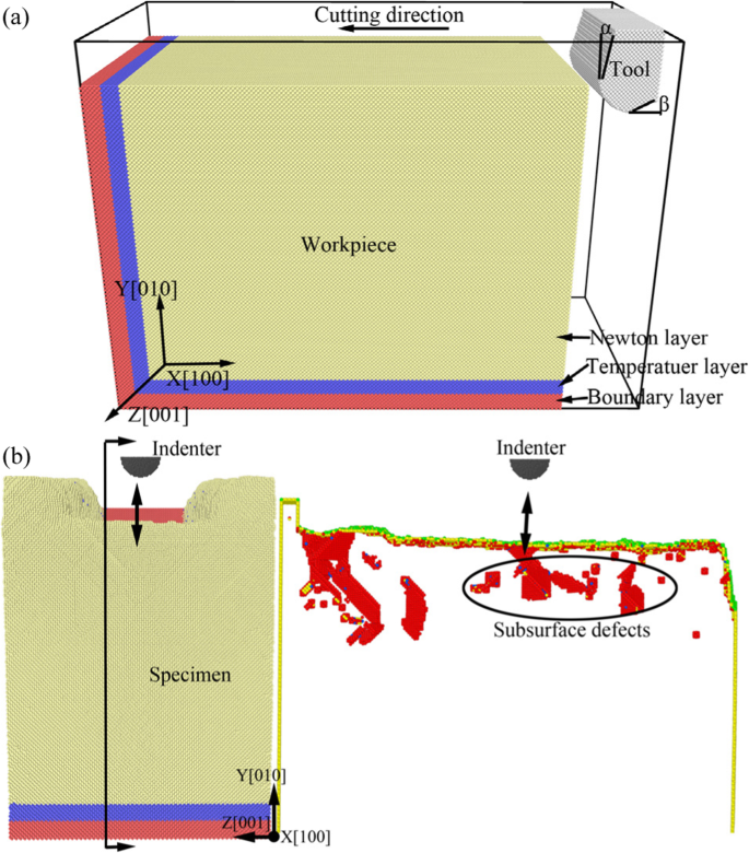
用于纳米切割和纳米压痕的单晶铜 3-D MD 模拟模型示意图。 一 纳米切割工艺模型。 b 含亚表面缺陷的纳米压痕工艺模型
原子间势函数
在本研究中,三维 MD 模拟由大规模原子/分子大规模并行模拟器 (LAMMPS) 执行。并行计算是在消息传递接口库的帮助下实现的。模拟中使用了莫尔斯势、嵌入原子法 (EAM) 势和 Tersoff 势,它们从 LAMMPS 软件包中调用。工件中的铜原子与刀具中的碳原子之间的相互作用是通过莫尔斯势计算的,如式(1)所示。 1 [23]。
$$ u\left({r}_{ij}\right)=D\left[\exp \left(-2\alpha \left({r}_{ij}-{r}_0\right)\right )-2\exp \left(-\alpha \left({r}_{ij}-{r}_0\right)\right)\right] $$ (1)其中 r 0, α , 和 D 分别是原子间距、弹性模量和结合能。数值如表2所示。
工件中铜原子之间的原子间函数用 EAM 势描述,如方程 1 所示。 2, 3 [24, 25]。
$$ E=\sum \limits_i^N\left[F\left({\rho}_i\right)+\sum \limits_{j>i}^Nu\left({r}_{ij}\right) \right] $$ (2) $$ {\rho}_i=\sum \limits_jf\left({r}_{ij}\right) $$ (3)金刚石工具中碳原子之间的相互作用由 Tersoff 势计算,如方程式 1 所示。 4, 5 [26]。
$$ E=\frac{1}{2}\sum \limits_{i\ne j}{V}_{ij} $$ (4) $$ {V}_{ij}={f}_c\left ({r}_{ij}\right)\left[{V}_R^{\hbox{'}}\left({r}_{ij}\right)+{b}_{ij}{V} _A\left({r}_{ij}\right)\right] $$ (5)其中 f c (r ij ) 是原子间的截断函数,V A (r ij ) 是吸收项的双势,V R (r ij ) 是排斥项的对偶势,r ij 是原子 i 之间的原子距离 和原子 j .
缺陷分析方法
在单晶铜的纳米切割中,变形和位错在工件表面下成核。在本文中,引入中心对称参数(CSP)来分析工件的位错形核和缺陷演化。对于面心立方 (FCC) 材料,CSP 值可以通过公式计算。 6 [27]。
$$ CSP=\sum \limits_{i=1}^6{\left|{R}_i+{R}_{i+6}\right|}^2 $$ (6)其中 R 我 是相同长度的相邻原子和 R i+6 是相反方向的相邻原子。 FCC晶体、部分位错、堆垛层错和表面原子的CSP值分别为0、2.1、8.3和24.9[27]。
CSP方法能够识别原子交错,但不能识别工件的局部原子晶体结构状态。因此,引入了共同邻居分析(CNA)来识别局部晶体结构缺陷。在 Honeycutt 和 Andersen [28] 提出的原始 CNA 方法中,各种结构用图表表示。目前,OVITO [29] 中有五种 CNA 模式,其中局部晶体结构被确定为面心立方 (FCC)、密排六方 (HCP)、体心立方 (BCC)、二十面体 (ICO)、和未知,分别。在本文中,还引入了位错提取算法(DXA)[30]来分析位错缺陷的演变。通过DXA,工件中不同的晶体结构会用不同的颜色标记,工件中的位错缺陷会用不同颜色的线条表示。
结果与讨论
纳米切割过程中的次表面缺陷演变
在纳米切削加工中,刀具在刀具对工件的挤压和剪切作用下,去除与切削深度相同厚度的工件表面材料,形成具有一定尺寸精度和表面质量的新加工表面。伴随能量转换和应力集中,工件表面和亚表面发生包括应力变形和热变形在内的复杂弹塑性变形。因此,形成亚表面损伤层并去除芯片。图2显示了单晶铜纳米切割过程中亚表面缺陷演变和材料去除的即时视图。在图 2 中,原子由 CSP 和 CNA 分析结果的值着色。在图 2a 和 c 中,黄色、绿色、红色和蓝色原子是表面原子、表面缺陷原子、次表面缺陷原子和 FCC 原子。从图 2 可以看出,在纳米切削加工过程中,工件表面下会形成大量典型的缺陷结构,如点缺陷、空位缺陷、堆垛层错、团簇缺陷、棱柱位错和螺旋位错环等。
<图片>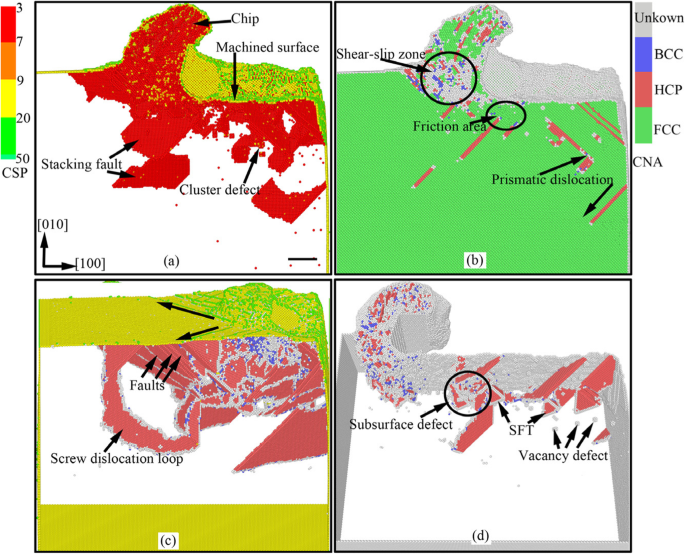
单晶铜纳米切割过程中亚表面缺陷演变的即时视图(在线颜色,比例尺 5 nm)。 a的切割距离 , b , c , 和 d 分别为18 nm、18 nm、6 nm和32 nm
由于刀具的挤压和剪切作用,在纳米切削过程中,前刀面前的原子产生剪切滑移变形,在工件内部形成初级剪切滑移区,如图. 2b.这些原子中的一些沿着前刀面向上滑动,形成如图 2a 所示的切屑。一些向下移动,加工表面在刀具侧面的挤压摩擦下形成,如图 2b 所示。其他部分向内移动并形成次表面缺陷,如堆垛层错、团簇缺陷和棱柱位错,如图2a和b所示。
由于刀具后刀面的摩擦和挤压,后刀面附近的原子发生能量积累,变成高能原子。当原子能超过一定水平时,高能原子所携带的能量就会释放出来,在高能原子的驱动下形成位错。因此,在侧面摩擦区域形成了大量位错,如图2d所示。随着加工表面的形成,位错在表面下成核、延伸和湮灭。最后,缺陷结构如堆垛层错、SFT 和空位缺陷留在地下,如图 2d 所示。堆垛层错在刀具下方的剪切滑移区成核,然后扩展到工件内部,最后在工件自由表面湮灭。最终,在工件表面形成位错线。位错线沿着\( \left[\overline{1}0\overline{1}\right] \), \( \left[\overline{1}01\right] \), 和[101]方向。位于剪切滑移带边缘的螺旋位错环由若干层错层和一系列螺旋位错组成。螺旋位错是在剪切滑移区压缩应力状态的驱动下形成的[11]。
在纳米切削过程中,位错在刀具的作用下成核和延伸。伴随着能量的聚集和释放,切削力随着切削距离的增加而波动,如图3的三个维度所示。在图 3 中,黑色、红色和蓝色曲线分别是进给力 (Fx)、后退力 (Fy) 和切向力 (Fz)。从图 3 可以看出,切削过程分为初始切削阶段和稳定切削阶段两个阶段。在初始切削阶段,进给力和后退力呈直线快速增加。进给力的最大值达到了 1100 nN 以上,但反作用力刚好达到 600 nN 左右。当刀尖完全切入工件时,就形成了加工面,如图3中第一个标记为加工面的小图所示。然后,纳米切削过程转移到稳定切削阶段。在稳定切割阶段,三个力都在它们的平衡位置波动。平均进给力约为 1000 nN,平均后退力仅为 500 nN 左右。从图 3 可以看出,进给力在 20 nm 的切削距离处迅速下降。这是因为能量积累达到了一定程度,即临界晶格应变能,如图 3 中的第二个小图所示。 同时,很大的阻力作用在刀具上,导致切削力为一个峰值。然后,能量被释放,导致位错发射,切削力减小,如图 3 中的第三个小图所示。因此,在稳定切削阶段,切削力是波动的。位错的形核、延伸和湮灭导致切削力的波动,最终导致工件内部存在次表面缺陷。
<图片>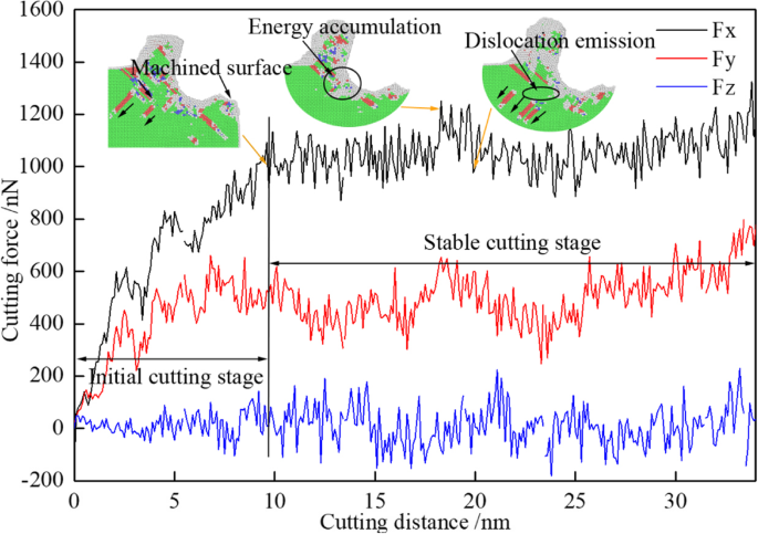
切削力随切削距离的变化曲线(彩色在线)。黑色、红色和蓝色曲线分别为进给力(Fx)、后退力(Fy)和切向力(Fz)
为了详细研究纳米切削过程中工件表面下位错缺陷的演变和特征,采用CNA方法对位错分布及其随切削距离的变化进行了细致的分析。工件某区域次表面缺陷演化如图4所示,其中图4a、b、c、d、e、f的切割距离分别为8 nm、10 nm、12 nm、20 nm 、24 nm 和 32 nm。由图 4a 可以看出,在切削过程的初始阶段,在刀具的挤压剪切作用下,大量的位错缺陷在剪切滑移区形核。特别是在原子应力和能量的驱动作用下,剪切滑移区形成了V型位错和断层,如图4b所示。在后续的加工过程中,随着刀具的不断移动,剪切滑移区向前移动。由于变形能的降低,断层逐渐消失。在刀具不断前进的过程中,后刀面摩擦带向断层附近移动。并且在后刀面的挤压和摩擦下形成粗糙的加工表面。然后故障继续湮灭并逐渐从工件表面脱离,如图4d所示。最后,故障转化为簇状缺陷,稳定存在于工件表面。同样,形成的V型位错在两个堆垛层错和一个位错锁的相互作用下逐渐演化为SFT。这些稳定的缺陷由次表面变形层组成,如图4e和 图4f所示。
<图片>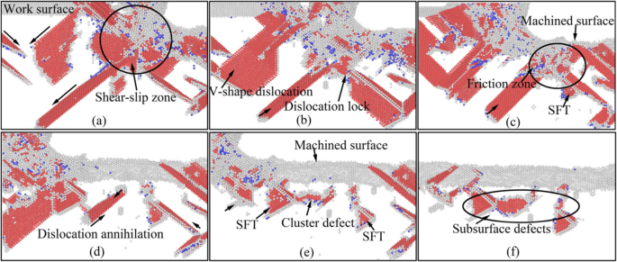
工件的次表面缺陷演变(在线颜色)。 a的切割距离 , b , c , d , e , 和 f 分别为8 nm、10 nm、12 nm、20 nm、24 nm和32 nm
众所周知,会发生残余应力释放和内部缺陷恢复 时效处理后的工件上。在实际的纳米加工中,加工过程中形成的一些亚表面缺陷会在加工过程中消失。为了模拟时效处理后的工件状态,对切削系统进行长时间的分子动力学弛豫。工件表面下经过长时间MD弛豫的残余缺陷分布图如图5所示,其中原子根据CSP和CNA方法的分析结果进行了着色。从图 5 可以看出,初级位错在弛豫后消失。工件表面下存在空位缺陷、堆垛层错、原子团簇、棱柱位错、螺旋位错、SFT、阶梯位错等,如图5所示。复杂内应力的诱发和位错缺陷的相互作用,将影响纳米加工后工件的尺寸精度和表面质量。
<图片>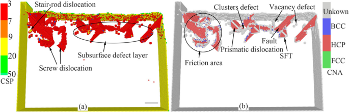
纳米切割后工件亚表面残留缺陷分布(彩色在线,比例尺5 nm)。 一 黄色、绿色、红色和蓝色原子是表面原子、表面缺陷原子、次表面缺陷原子和 FCC 原子。 b 绿、红、灰、蓝原子分别为FCC、HCP、未知、BCC结构
具有机加工引起的次表面缺陷的铜样品的纳米压痕测试
加工引起的次表面残留缺陷控制着表面的机械性能,尤其是硬度和杨氏模量。因此,研究纳米压痕过程中位错的成核和相互作用似乎非常必要。为了研究加工引起的亚表面缺陷对单晶铜力学性能的影响,采用与纳米切割模拟相同的参数对纳米切割后的试样进行纳米压痕工艺。仿真结果如图 1 和图 5 所示。 6、7、8、9和10。纳米压痕初始状态下表面缺陷分布的瞬时原子图如图6所示。从图中可以看出有几个SFTs,一个V形位错、一些棱柱位错和一些压头下方的簇缺陷。这些亚表面缺陷会影响工件在纳米压痕过程中的位错形核和扩展。进而改变工件材料的力学性能。
<图片>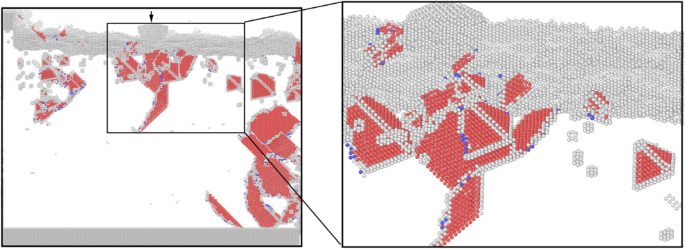
初始压痕状态下工件表面缺陷分布(在线颜色)。红、灰、蓝原子为HCP、未知、BCC结构
<图片>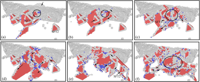
纳米压痕加载过程中亚表面位错缺陷演化(彩色在线)。 a对应的压痕深度 –f 分别为0 nm、0.5 nm、1 nm、2 nm、3 nm和4 nm
<图片>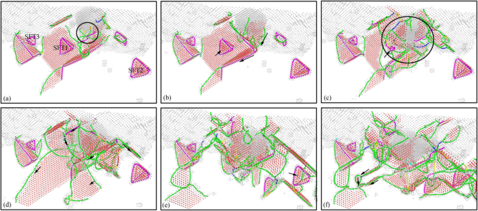
纳米压痕加载过程中亚表面位错的分布(彩色在线)。 a对应的压痕深度 –f 分别为 0 nm、0.5 nm、1 nm、2 nm、3 nm 和 4 nm。配色方案:深蓝色为完美位错,绿色为肖克利位错,粉红色为阶梯型位错,黄色为赫斯位错,浅蓝色为弗兰克位错,红色为不明位错
<图片>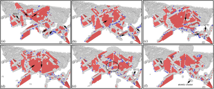
纳米压痕卸载过程中亚表面缺陷演变(彩色在线)。 a对应的压痕深度 -f分别为4 nm、3 nm、2 nm、1 nm、0 nm和-1 nm
<图片>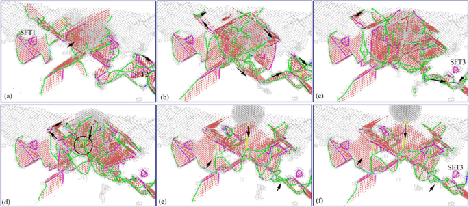
纳米压痕卸载过程中亚表面位错的分布(彩色在线)。 a对应的压痕深度 –f 分别为4 nm、3 nm、2 nm、1 nm、0 nm和-1 nm。配色方案:深蓝色为完美位错,绿色为肖克利位错,粉红色为阶梯型位错,黄色为赫斯位错,浅蓝色为弗兰克位错,红色为不明位错
纳米压痕加载过程中次表面位错的原子演化图如图 7 所示。 从图 7a 可以看出,当压头接触试样表面时,位错的初始形核发生在试样表面。样品。随着压头的向下压力,形核位错逐渐扩大。同时,在压头施加的应力的影响下,大量位错成核并沿滑移系统移动,如图7b所示。在新形成的位错与原有亚表面缺陷的相互作用下,一些简单的缺陷逐渐消失,而V型位错则继续逐渐演化和湮灭。压头下的 SFT 逐渐减小,如图 7c 所示。随着压痕过程的进行,新的成核位错缺陷的规模增加,V型位错和压头下的SFT1逐渐消失。同时,压痕过程中形成的位错缺陷逐渐演化为棱柱形位错环,其中堆垛层错逐渐消失,如图7d所示。新形成的棱柱位错环继续延伸到压头右下方的 SFT2。由于其稳定的结构,SFT2 在棱柱位错环的扩展过程中保持不变形,如图 7e 所示。随着压头的下压,棱柱位错环继续向下扩展,亚表层位错缺陷的规模逐渐增大。 SFT2结构稳定存在于试样的亚表面,在位错缺陷的移动和干涉过程中没有发生变化,如图7 f所示。
为了更清楚地显示压痕过程中次表面缺陷的演变和分布,采用DXA方法对压痕后的试样进行分析。由DXA分析得到图7对应各时刻的次表面位错分布图,如图8所示。位错按以下方案着色:深蓝色为完美位错,绿色为肖克利位错,粉色为Stair-rod位错,黄色为 Hirth 位错,浅蓝色为 Frank 位错,红色为未识别位错。
从图 8 可以看出,工件亚表面在初始压痕状态下主要由 Shockley 位错和 Stair-rod 位错组成。存在于地下的 SFT 是由 6 个楼梯杆位错组成的规则四面体结构。当压头接触工件时,工件表面的位错形核为黄色Hirsh位错,如图8a所示。随着压头下压,大量位错成核并沿滑移系统移动。黄色的Hirsh 位错逐渐变为绿色的Shockley 位错,如图8b 所示。在新形成的位错与原始 SFT1 的相互作用下,一些简单的位错逐渐消失,如图 8c 所示。次表面位错的规模随着压头的下降而增加,新形成的位错主要是绿色Shackley位错。肖克利位错和 SFT1 之间的相互作用导致 SFT1 的大小逐渐减小并最终消失,如图 8d 所示。随着缺陷规模的增加,试样表面下位错的数量和类型也随之增加。地表下形成红色未知类型的位错,多个肖克利位错构成棱柱位错环,如图8e所示。在Shockley位错和Stair-rod位错的相互作用下,由于压头的挤压较弱,远离压痕区域的SFT2和SFT3最终没有消失,如图8f所示。
纳米压痕卸载过程中亚表面位错的演化图像如图9所示。图10为图9对应的亚表面位错分布图。从两张图中可以看出亚表面缺陷的规模增加开始,然后在压头向上移动的过程中逐渐减小。它是由材料变形能的持续释放与压头对试样施加的粘附力之间的综合作用引起的。在卸载过程的初始阶段,压头效应对试样的向上吸附力不显着。 The evolution of subsurface defect is mainly driven by the material deformation energy, which results in the scale of subsurface defects increase. And the main types of dislocations in the stage are the green Shockley dislocation and the pink ladder dislocation, as shown in Figs. 9a, b and 10a, b. The interaction between the SFT2 and Shockley dislocation nearby makes pink stair-rod dislocation turn into green Shackley dislocation in the area far away indenter action. Meanwhile, the SFT2 is transformed into a smaller defect which is SFT3, as shown in Figs. 9c and 10c. With the continuous lifting of the indenter, the bonding and adsorbing effect exerted by the indenter on the specimen increases gradually. Accompany with the deformation energy release, the size and types of dislocations in subsurface increase. And more perfect dislocations, Hirh dislocations, and unknown dislocations are formed, as shown in Figs. 9d and 10d. In later stage of unloading process, the material deformation energy is basically released, and the evolution of subsurface defects is dominated by the adsorption from the indenter. Therefore, the subsurface defects are annihilated rapidly, and the scale of subsurface defects decreases rapidly. And a typical Hirsch dislocation is formed in the direction of the indenter upward, which is shown in Figs. 9e, f and 10e, f. Finally, the scale of subsurface defects decreases considerably, and some typical subsurface defects, such as SFT and atomic clusters, are gradually disappeared. From the above analysis, it can be seen that secondary processing (nano-indentation) can restore the typical internal defects formed in nano-cutting, and the subsurface damage becomes more serious in the secondary processing area. These characteristics of subsurface defects will affect the mechanical properties of materials. Hence, it is necessary to study the effect of subsurface defects on the mechanical properties of material.
Mechanical properties of materials can be calculated by load-displacement curve, such as hardness, elastic modulus, and yield strength. In this study, hardness and Young’s modulus of single crystal copper were investigated. The variation of load on the indenter was monitored during the nano-indentation process, and the load-displacement curve of the nano-indentation process was drawn, as shown in Fig. 11. The max indentation depth of the red and black curves respectively is 2 nm and 3 nm, in which both loading and unloading processes are included. The upward direction of load is defined as positive direction, so the load-displacement curves are all above the zero line in the process of loading, while the load on the indenter changes from positive to negative during unloading. The elasticity restore of deformed matrix material exerts an upward force on the indenter. Therefore, in order to keep the indenter raising in uniform speed, a downward force (positive) is required. With the gradual recovery of deformation, the force gradually decreases until it disappears. Then the force applied on the indenter becomes negative, and the absolute value of the force first increases and then decreases. From the graph, it can be seen that the specimen is in the stage of elastic deformation during loading process, and the load increases in proportion to the displacement. When the displacement of the indenter is 1 nm, the load on the indenter is fluctuated dramatically, as indicated by the arrow on the left side of Fig. 11. This is because that the indenter is pressed down to the SFT1 shown in Fig. 7, which results in the greater impediment to the indenter. When the indenter displacement is in the range of 2 to 3 nm, the fluctuation amplitude of the load increases. This is because the indenter is pressed down to the SSD layer, and the impediment of the indenter to the subsurface defect in the specimen is more significant, so the fluctuation amplitude of the load increases significantly.

Load-displacement curve of nano-indentation on the machining-induced specimen (color online). The maximum indentation depth of the black curve and the red curve respectively is 3 nm and 2 nm
According to Oliver-Pharr Method [31], nano-indentation hardness can be defined as indentation load divided by the contact area between indenter and specimen, which is calculated by Eq. 7.
$$ H={F}_{\mathrm{max}}/{A}_c $$ (7)In which, F max is the peak value of the load. A c is projected contact area for indenter and specimen, which can be obtained by
$$ {A}_c=\pi {r}^2 $$ (8)其中 r is contact radius for indenter. Because the indenter is hemispherical in shape, r is approximately equal to indentation depth.
The elastic deformation of single crystal copper material is caused by the load exerted from indenter. Based on the previous load-displacement curve, Young’s modulus (E ) of single crystal copper can be calculated by Eq. 9.
$$ E=\frac{\sigma }{\varepsilon }=\frac{F/S}{DL/L}=\frac{F/\pi {r}^2}{DL/L} $$ (9)其中 F is applied load, S is contact area, r is projection radius of indenter, DL is material deformation along loading direction, which is equal to indentation depth, and L is the total length of material along loading direction. In this study, L is equal to 30 nm.
According to the Oliver-Pharr method and load-displacement data, nano-indentation hardness and Young’s elastic modulus of single crystal copper materials with subsurface defects can be calculated based on Eqs. 7, 8, 9. Table 3 shows the applied load acting on the specimens by indenter with different indentation depths.
The nano-indentation hardness of single crystal copper can be calculated by Eqs. 7 and 8 combining the data in Table 3. When the maximum depth is 2 nm, F max =190.67 nN and from Fig. 11 r =2.75 nm. The calculated value of nano-indentation hardness H2 is 8.029 GPa. When the maximum depth is 3 nm, F max =244.66 nN and r =3 nm. The calculated value of nano-indentation hardness H3 is 8.675 GPa, which is slightly larger than it obtained at indentation depth of 2 nm. It is because the indenter is pressed down to the subsurface defects area at indentation depth of 3 nm, and the deformation resistance of the subsurface defects increases. Therefore, the hardness of the single crystal copper increased. It can be concluded from the result that the subsurface defects make the machined surface much harder, which is work-hardening phenomenon.
The Young’s modulus E of single crystal copper can be calculated by Eq. 9 combining the data in the Table 3. The calculation results are shown in Table 4. It can be noted that the Young’s modulus becomes distinctly higher when the indentation depth is smaller than 1.5 nm. In the initial stage of nano-indentation, the indenter does not contact the defects residual area in subsurface. However, the work-hardening effect makes the specimen material not easily be occurred elastic deformation; therefore, the Young’s modulus of single crystal copper is larger in the initial stage of indentation. The value of Young’s modulus is 119.4 GPa when indentation depth is 2 nm, which is almost the same with Zhang’s research (120.4 GPa) [14]. With the increase of indentation depth, the Young’s elastic modulus of single crystal copper specimens decreases gradually, and the ability of materials to resist elastic deformation is weakened. It is due to the permanent elastic deformation is derived from the dislocation motion and its interaction with subsurface defects. It has been revealed that the nano-cutting-induced subsurface defects will affect the physical and mechanical properties of single crystal copper materials, which is also applicable to other FCC materials. The existence of subsurface defects will enhance the hardness of machined surface and weaken the ability of material to resist elastic deformation, in which the mutual evolution between dislocations and subsurface defects plays an important role. Therefore, it is very important to predict the thickness of subsurface deformation layer and study the surface properties for nano-fabrication.
结论
The subsurface defects stable exist in workpiece after nano-cutting can affect the mechanical properties, which is critical to the service performance and life of nano-structures. The previous studies are mainly based on perfect crystal materials or artificial constructing hypothetical defects, which is far from the actual subsurface defects. In this paper, molecular dynamics simulation of nano-cutting is performed to construct the specimen model with subsurface defects. Based on the built MD model, nano-indentation simulation is carried out to study the influence of machining-induced subsurface defects on the physical and mechanical properties of single crystal copper materials. The interaction mechanism between dislocation and complex defects during nano-indentation is studied. The nano-indentation hardness and Young’s elastic modulus of single crystal copper materials are calculated. Based on the above analysis, some interesting conclusions can be drawn as follows.
- 1.
The dislocation nucleation and expansion in workpiece subsurface are driven by the extrusion and shearing action of cutting tool during the nano-cutting process, which results in the fluctuation of cutting force. After nano-cutting, there are stable defect structure residues in the subsurface of workpiece, such as vacancy defects, stacking faults, atomic clusters, SFT, and stair-rod dislocations, which together constitute the subsurface defect layer of workpiece.
- 2.
The existence of subsurface defects affects the nucleation and expansion of dislocations during nano-indentation process. Some stable defects directly below the indenter, such as V-shaped dislocation and SFT1, are annihilated after indentation. And SFT2 far from the indentation region is transformed into a smaller one. Secondary processing of nano-indentation can restore typical internal defects of the workpiece, but the subsurface defects in the secondary processing area are aggravated.
- 3.
The nano-indentation hardness of specimens increases with the introduction of subsurface defects, which results in the formation of work-hardening effect. The Young’s modulus of single crystal copper is larger in the initial stage of indentation and gradually decreases with the increase of indentation depth. The existence of subsurface defects can weaken the ability of material to resist elastic deformation, in which the mutual evolution between dislocations and subsurface defects plays an important role.
数据和材料的可用性
The conclusions made in this manuscript are based on the data which are all presented and shown in this paper.
缩写
- MD:
-
Molecular dynamics
- SSD:
-
Subsurface defects
- SFT:
-
Stacking fault tetrahedral
- PBC:
-
Periodic boundary condition
- LAMMPS:
-
Large-scale atomic/molecular massively parallel simulator
- EAM:
-
Embedded-atom method
- CSP:
-
Centro-symmetry parameter
- FCC:
-
Face center cubic
- CNA:
-
Common neighbor analysis
- HCP:
-
Close-packed hexagonal
- BCC:
-
Body centered cubic
- ICO:
-
Icosohedral
- DXA:
-
Dislocation extract algorithm
纳米材料
- 3D 打印材料市场的演变:2019 年的趋势和机遇
- SLS 的演变:新技术、材料和应用
- 工程师如何评估塑料材料和材料强度?
- 通过溶胶-凝胶工艺制备的纳米结构二氧化硅/金-纤维素-键合氨基-POSS 混合复合材料
- 接触非平衡等离子体对 Mn Х Fe3 − X О4 尖晶石结构和磁性能的影响
- 富勒烯衍生纳米材料及其聚合物复合材料的顺磁特性:剧烈泵出效应
- 石墨烯和多壁碳纳米管对 Cu/Ti3SiC2/C 纳米复合材料的微观结构和机械性能的协同作用
- 通过蒸发诱导自组装和增强的气敏特性简便合成虫孔状介孔氧化锡
- 工程材料的特性:一般、物理和机械
- 材料的 14 种不同机械性能列表
- 用于冲头的钢材和工具的性能
- 不同类型的材料机械性能