

通过有限元撕裂和互连方法有效预测和分析纳米尺度的光学俘获
摘要
数值模拟对于基于等离子体纳米光镊的光俘获预测具有重要作用。然而,等离子体效应的复杂结构和剧烈的局部场增强给传统的数值方法带来了巨大的挑战。在本文中,提出了一种基于双原始有限元撕裂和互连(FETI-DP)和麦克斯韦应力张量的准确有效的数值模拟方法,以计算捕获纳米粒子的光学力和潜力。引入了低秩稀疏化方法以进一步提高 FETI-DP 模拟性能。该方法通过使用非重叠域划分和灵活的网格离散化,将大规模复杂问题分解为小规模简单问题,具有较高的效率和并行性。数值结果表明了该方法在纳米尺度光学俘获预测和分析中的有效性。
介绍
基于表面等离子体激元 (SP) 的等离子体光镊引起了广泛关注,并已广泛应用于捕获纳米粒子 [1,2,3,4,5,6]。 SP 是由特定波长的入射光和自由电子在金属和电介质的界面耦合引起的共振现象 [7]。 SP 使光镊能够突破衍射极限。此外,SP 的剧烈局部场增强可以降低对入射光强度的需求 [7, 8]。然而,SPs与物体的材料和尺寸以及入射光的波长密切相关,在实践中需要大量的实验来确定SP光镊的最佳参数。基于此,仿真方法作为SP光镊设计和优化的辅助手段发挥着越来越重要的作用[9]。在这些模拟中,需要计算光学力来预测稳定的俘获。对于球体等规则物体,可以从广义 Lorenz-Mie 理论 [10, 11] 解析导出光学力。然而,对于具有复杂构型的物体,需要采用严格求解控制麦克斯韦方程组的数值方法来对电磁场以及随后的光力和势进行建模。
这些数值方法主要可分为微分方程法 (DEM) 和积分方程法 (IEM) [12,13,14,15]。与 IEM 相比,微分方程方法 (DEM) 在处理复杂的几何形状和组件方面表现出卓越的能力。 DEM 还具有直接计算近场分布的优势,这在 SP 分析中起着重要作用。作为具有代表性的 DEM,在时域中实现了有限差分时域 (FDTD) 方法,可以轻松获取宽带信息和瞬态响应 [16, 17]。然而,FDTD 需要一个准确的色散模型来描述 SP 中与频率相关的材料特性,而 FDTD 求解精度在很大程度上取决于该色散模型的近似精度 [18]。此外,FDTD 依赖于结构化网格,这通常会导致曲面的阶梯误差。作为另一种代表性的 DEM,有限元法 (FEM) 已被广泛采用,因为它可以轻松处理频域中的色散材料并通过非结构化网格消除阶梯误差 [19,20,21,22]。与FDTD相比,FEM可以直接采用实测材料参数,无需任何近似色散模型。然而,SP 中的剧烈局部场增强需要 FEM 离散化中的精细网格。此外,具有大尺寸和多个对象的对象会显着增加未知数。这些因素会导致矩阵系统病态和巨大的计算消耗,这给传统有限元法对SP增强光学俘获的分析带来了巨大挑战。
在本文中,介绍了一种有效的双原始有限元撕裂和互连 (FETI-DP) 方法来模拟纳米级的光学俘获。 FETI-DP采用非重叠域分解方案,将一个原始的大规模复杂问题分解为一系列小规模的简单问题来克服它们。它在子域接口处强制传输条件以确保场连续性,并引入对偶变量以通过拉格朗日乘子将原始三维(3D)问题简化为二维(2D)问题。提取子域角处的原始变量以加快对偶问题迭代求解的收敛速度[23,24,25,26]。开发了一种低秩稀疏化方法来提高 FETI-DP 的性能。它使用数据稀疏算法来提高解决子域问题和对偶问题的效率 [27, 28]。所提出的方法提供了完全解耦的子域,从而能够并行模拟用于捕获纳米粒子的光学力。麦克斯韦应力张量(MST)揭示了电磁场和机械动量之间的关系,用于评估光学力[29]。基于获得的光力,可以进一步计算光势以分析稳定捕获。与IEMs相比,所提出的方法在处理复合材料和解决基于SP的光阱的近场问题上更强大。与FDTD相比,所提出的方法可以准确处理基于SP的光学俘获系统中的色散金属材料,并消除具有曲线边界的物体的阶梯误差。与有限元法相比,所提出的方法适用于光学捕获的大规模计算。对几个例子进行了分析,数值结果证明了所提出的方法在纳米尺度光阱预测和分析中的准确性和有效性。
方法
FETI-DP 配方
对于FETI-DP实现,原始计算域Ω首先被撕成一系列不重叠的子域Ω i (i =1, 2, 3⋯, N s ),如图1所示。在每个子域Ω i ,从矢量波动方程可以推导出子域有限元系统
$$ \nabla \times {\mu}_r^{-1}\nabla \times {\mathbf{E}}^i-{k}_0^2{\varepsilon}_r{\mathbf{E}}^i ={jk}_0{\eta}_0{\mathbf{J}}_{\mathrm{imp}}^i\kern1.08em \mathrm{in}\kern0.24em {\Omega}^i $$ (1 ) $$ \hat{n}\times \nabla \times {\mathbf{E}}^i+{jk}_0\hat{n}\times \left(\hat{n}\times {\mathbf{E} }^i\right)=0\kern0.96em \mathrm{on}\kern0.24em {\Gamma}_{\mathrm{ABC}}^i $$ (2)
FETI-DP 方法中具有非重叠子域的域划分方案。 一 原始域。 b 划分子域和离散网格
其中 E i 表示在 \( {\Omega}^i \), k 中待解的未知电场 0 和 η 0 分别是自由空间波数和固有阻抗,\( {\mathbf{J}}_i^{\mathrm{imp}} \) 是外加电流。 \( {\Gamma}_{\mathrm{ABC}}^i \) 表示吸收边界条件 (ABC) 来截断无限开放区域。需要注意的是 k 如果周围介质不是自由空间,则应将 0 替换为介质中的波阻抗,这对于光捕获来说很常见。在子域接口Γ i ,需要一个假设的边界条件来生成Ω i中的完整边界值问题 .这里,具有未知辅助变量Λ的Robin型传输条件 我 被强制为
$$ {\hat{n}}^i\times \left({\mu}_r^{-1}\nabla \times {\mathbf{E}}^i\right)+{\alpha}^i{ \hat{n}}^i\times \left({\hat{n}}^i\times {\mathbf{E}}^i\right)={\boldsymbol{\Lambda}}^i\kern1. 2em \mathrm{on}\kern0.36em {\Gamma}^i $$ (3)其中\( {\hat{n}}^i \) 表示子域界面Γ i 处的单位法向外向矢量 , 和 α i 是一个复杂的参数,通常可以选择为 jk 0. 然后所有子域都由四面体元素离散化。在每个元素中,我们展开 E 带有向量基函数 N 和未知的电场系数E 如
$$ \mathbf{E}=\sum \limits_{p=1}^s{E}_p{\mathbf{N}}_p $$ (4)其中 s 表示每个四面体元素中向量基函数的数量。 s 传统的基于边缘的低阶基函数选择为6,而高阶向量基函数由于引入了基于面或体积的附加基函数,因此选择较大。
应用伽辽金方法,Ω i中的有限元矩阵方程 关于未知电场系数E i 可以得到
$$ \left(\begin{array}{cc}{\mathbf{K}}_{rr}^i&{\mathbf{K}}_{rc}^i\\ {}{\mathbf{K}} _{cr}^i&{\mathbf{K}}_{cc}^i\end{array}\right)\left(\begin{array}{l}{E}_r^i\\ {}{E }_c^i\end{array}\right)=\left(\begin{array}{l}{f}_r^i-{\mathbf{B}}_r^{i^T}{\lambda}^ i\\ {}{f}_c^i\end{array}\right) $$ (5)其中下标符号 c 和 r 区分角自由度 (DOF) 和剩余自由度,提取角自由度作为原始变量来构建对偶原始 (DP) 方案。在这里,K 是 FEM 系统矩阵和 f 是激励向量。 B 是一个布尔矩阵,用于提取子域的界面自由度。 λ 是由扩展Λ产生的对偶变量 我 ,也称为拉格朗日乘子。
然后,相邻的子域可以通过在界面处增强切向电场和磁场的连续性来互连。我们组装所有子域接口并消除所有子域内部未知数E i .一个关于双变量λ的简化全局接口方程 可以得到
$$ \left[{\tilde{\mathbf{K}}}_{rr}+{\tilde{\mathbf{K}}}_{rc}{\tilde{\mathbf{K}}}_{cc }^{-1}{\tilde{\mathbf{K}}}_{cr}\right]\lambda ={\tilde{f}}_r-{\tilde{\mathbf{K}}}_{rc }{\tilde{\mathbf{K}}}_{cc}^{-1}{\tilde{f}}_c $$ (6)等式(6)可以通过迭代方法求解,例如广义最小残差(GMRES)方法。 \( {\tilde{\mathbf{K}}}_{cc} \) 是全局角系统,可以加速原始空间的迭代收敛。可以使用合适的预处理器来提高迭代收敛速度,例如近似逆和不完全 LU 分解。一旦对偶变量λ 求解后,每个子域内的电场可以通过(5)独立评估。对于全局矩阵 \( {\tilde{\mathbf{K}}}_{rr} \) 的构造,需要构造子域数值格林函数 \( {\mathbf{Z}}_{rr}^ i \) 形式为
$$ {\mathbf{Z}}_{rr}^i={\mathbf{B}}_r^i{\left({\mathbf{K}}_{rr}^i\right)}^{- 1}{{\mathbf{B}}_r^i}^T $$ (7)其中包括子域 FEM 矩阵 \( {\left({\mathbf{K}}_{rr}^i\right)}^{-1} \) 的逆矩阵。此外,对于矩阵 \( {\tilde{\mathbf{K}}}_{rc} \), \( {\tilde{\mathbf{K}}}_{cr} \) 和 \( {\tilde {\mathbf{K}}}_{cc} \) 和向量 \( {\tilde{f}}_r \) 和 \( {\tilde{f}}_c \),\( {\left({ \mathbf{K}}_{rr}^i\right)}^{-1} \) 需要计算。 \( {\left({\mathbf{K}}_{rr}^i\right)}^{-1} \) 在预处理阶段的构造以及它们在迭代求解阶段的计算成本很高。虽然 \( {\mathbf{K}}_{rr}^i \) 是稀疏的,\( {\left({\mathbf{K}}_{rr}^i\right)}^{-1} \ ) 是密集的,这意味着高计算成本。接下来,引入低秩稀疏化方法来加速 \( {\left({\mathbf{K}}_{rr}^i\right)}^{-1} \) 的计算。由于全局接口系统中的一些子矩阵可以用低秩矩阵的形式表示,它们的计算可以用低秩算法进行,从而提高了FETI-DP的性能。可以看出,FETI-DP 提供了独立的子域操作,因此可以利用并行计算来提高效率。对于一个高效的并行方案,域划分的一个原则是使每个子域中的自由度数量尽可能均衡。因此,子域的大小应与网格离散化密度相关。通常,细网格区域采用小子域,粗网格区域采用大子域。
低秩稀疏化
提出了一种低秩稀疏化方法,以提供一种数据稀疏方法来提高 FETI-DP 效率。在这里,数据稀疏 意味着这些矩阵实际上不是稀疏的,但它们是稀疏的,因为它们的某些子块可以用低秩分解矩阵形式表示为
$$ \mathbf{M}={\mathbf{XY}}^{\mathrm{T}}\kern0.72em \left(\mathbf{M}\in {\mathrm{\mathbb{C}}}^{ m\times n},\mathbf{X}\in {\mathrm{\mathbb{C}}}^{m\times k},\mathbf{Y}\in {\mathrm{\mathbb{C}}} ^{n\times k}\right) $$ (8)其中 X 和是 是全矩阵形式,秩 k 远小于 m 和 n .矩阵 \( {\left({\mathbf{K}}_{rr}^i\right)}^{-1} \) 可以用数据稀疏矩阵形式表示,因为它具有积分的矩阵性质操作员。因此,如果 \( {\left({\mathbf{K}}_{rr}^i\right)}^{-1} \) 在给定的子域中具有低秩属性,它可以被有效地计算和存储在数据稀疏形式与低秩稀疏化方法,加速迭代解决方案中的MVP。
低秩稀疏化方法的过程可以分为以下步骤:(1)通过细分每个子域中的基函数集构建聚类树,(2)通过两个聚类树的相互作用构建块聚类树,( 3) 通过可接受条件生成 \( {\mathbf{K}}_{rr}^i \) 的数据稀疏形式, (4) 执行低秩格式化算法以获得 \( {\left({\mathbf{K}}_{rr}^i\right)}_{\mathrm{DS}}^{-1} \),和 (5) 输入 FETI-DP 系统的解由数据稀疏算法。可以使用合适的预处理器来加速求解。需要注意的是,数据稀疏LU分解\( {\left({\mathbf{K}}_{rr}^i\right)}_{\mathrm{DS}}={\left({\mathbf {L}}_{rr}^i\right)}_{\mathrm{DS}}{\left({\mathbf{U}}_{rr}^i\right)}_{\mathrm{DS} } \) 代替矩阵求逆\( {\left({\mathbf{K}}_{rr}^i\right)}_{\mathrm{DS}}^{-1} \)。采用嵌套解剖技术来进一步提高低秩稀疏化的效率。嵌套剖析使用分隔符产生大的非对角零子块,在LU分解过程中将保持为零,从而可以显着减少填充。
为了生成\( {\left({\mathbf{K}}_{rr}^i\right)}_{\mathrm{DS}} \),我们首先构造一个簇树T 我 通过递归细分子域基于边的基函数集I ={1,2,……N 使用边界框。通过嵌套解剖,一个簇 t 在对应的bounding box内分为三个后继{s 1, s 九月 , s 2},其中 s 1 和 s 2是两个断开的边界框的索引集和s 九月 是分隔符的索引集。图 2a 显示了此过程的一个简单示例。然后,一个块簇树T 我 × 我 可以通过交互两个簇树T来构建 我 ,如图2b所示,可以选择作为原始基于边的基函数集的聚类树和Galerkin方法中的测试基函数集的聚类树。接下来,我们需要引入一个基于嵌套剖析的可接受条件来区分T中的完整块、低秩分解块和非对角零块 我 × 我 [23]。因此,\( {\left({\mathbf{K}}_{rr}^i\right)}_{\mathrm{DS}} \) 可以通过用非零条目填充相应的块来产生\( {\mathbf{K}}_{rr}^i \)。最后,\( {\left({\mathbf{K}}_{rr}^i\right)}_{\mathrm{DS}}={\left({\mathbf{L }}_{rr}^i\right)}_{\mathrm{DS}}{\left({\mathbf{U}}_{rr}^i\right)}_{\mathrm{DS}} \ ) 可以从
递归计算 $$ {\mathbf{K}}_{rr}^i=\left[\begin{array}{ccc}{\mathbf{K}}_{11}&&{\mathbf{K}}_{13 }\\ {}&{\mathbf{K}}_{22}&{\mathbf{K}}_{23}\\ {}{\mathbf{K}}_{31}&{\mathbf{K }}_{32}&{\mathbf{K}}_{33}\end{array}\right]=\left[\begin{array}{ccc}{\mathbf{L}}_{11}&&\\ {}&{\mathbf{L}}_{22}&\\ {}{\mathbf{L}}_{31}&{\mathbf{L}}_{32}&{\mathbf{ L}}_{33}\end{array}\right]\left[\begin{array}{ccc}{\mathbf{U}}_{11}&&{\mathbf{U}}_{13} \\ {}&{\mathbf{U}}_{22}&{\mathbf{U}}_{23}\\ {}&&{\mathbf{U}}_{33}\end{array} \right] $$ (9)
基于嵌套解剖的4级簇树和块簇树的构建。 一 基于边的基函数集I递归细分构造聚类树 ={1,2,…18}。 b 构建一个块簇树,其中白色 块是零矩阵和绿色 块可以是满矩阵或低秩分解矩阵
其中传统的全矩阵算术被它们的数据稀疏对应物取代 [28]。自适应截断误差ε t 用于控制低秩近似的准确性。得到的LU因子\( {\left({\mathbf{L}}_{rr}^i\right)}_{\mathrm{DS}} \) 和\( {\left({\mathbf{U} }_{rr}^i\right)}_{\mathrm{DS}} \) 被存储并用于构造\( {\mathbf{Z}}_{rr}^i \) by
$$ {\mathbf{Z}}_{rr}^i={\mathbf{B}}_r^i{\left({\mathbf{U}}_{rr}^i\right)}_{\ mathrm{DS}}^{-1}{\left({\mathbf{L}}_{rr}^i\right)}_{\mathrm{DS}}^{-1}{\mathbf{B} }_r^i $$ (10)其中 \( {\mathbf{B}}_r^i{\left({\mathbf{U}}_{rr}^i\right)}_{\mathrm{DS}}^{-1} \) 和\( {\left({\mathbf{L}}_{rr}^i\right)}_{\mathrm{DS}}^{-1}{\mathbf{B}}_r^i \) 可以是由数据稀疏的上下三角求解器计算。 \( {\left({\mathbf{L}}_{rr}^i\right)}_{\mathrm{DS}} \), \( {\left({\mathbf{U}}_{ rr}^i\right)}_{\mathrm{DS}} \),和\( {\mathbf{Z}}_{rr}^i \) 进入FETI-DP计算,数据稀疏向前和向后替换 (FBS) 和数据稀疏 MVP。
光学力和势
根据电动力学理论,光学力可以通过麦克斯韦应力张量 (MST) 来评估,它揭示了电磁场和机械动量之间的关系 [29]。一旦获得了物体周围的电磁场分布,就可以通过在物体周围的封闭表面上对 MST 进行积分来计算光力。根据得到的电场分布,可以构造任意坐标处的MST
$$ \overleftrightarrow{\mathbf{T}}=\frac{1}{2}\operatorname{Re}\left[\varepsilon {\mathbf{EE}}^{\ast }+\mu {\mathbf{HH }}^{\ast }-\frac{1}{2}\left(\varepsilon {\left|\mathbf{E}\right|}^2+\mu {\left|\mathbf{H}\right |}^2\right)\overleftrightarrow{\mathbf{I}}\right] $$ (11)其中上标星号表示电场或磁场的共轭,ε 是 μ 是介电常数和磁导率,\( \overleftrightarrow{\mathbf{I}} \) 是一个 3 × 3 单位矩阵。由向量的外积,\( \overleftrightarrow{\mathbf{T}} \) 的张量形式可以写成
$$ \overleftrightarrow{\mathrm{T}}=\left[\begin{array}{lll}{T}_{xx}&{T}_{xy}&{T}_{xz}\\ {} {T}_{yx}&{T}_{yy}&{T}_{yz}\\ {}{T}_{zx}&{T}_{zy}&{T}_{zz} \end{array}\right]=\left[\begin{array}{ccc}\varepsilon {E}_x{E}_x^{\ast }+\mu {H}_x{H}_x^{\ast }-\frac{\varepsilon {\left|\mathbf{E}\right|}^2+\mu {\left|\mathbf{H}\right|}^2}{2}&\varepsilon {E} _x{E}_y^{\ast }+\mu {H}_x{H}_y^{\ast }&\varepsilon {E}_x{E}_z^{\ast }+\mu {H}_x{ H}_z^{\ast}\\ {}\varepsilon {E}_y{E}_x^{\ast }+\mu {H}_y{H}_x^{\ast }&\varepsilon {E}_y {E}_y^{\ast }+\mu {H}_y{H}_y^{\ast }-\frac{\varepsilon {\left|\mathbf{E}\right|}^2+\mu { \left|\mathbf{H}\right|}^2}{2}&\varepsilon {E}_y{E}_z^{\ast }+\mu {H}_y{H}_z^{\ast} \\ {}\varepsilon {E}_z{E}_x^{\ast }+\mu {H}_z{H}_x^{\ast }&\varepsilon {E}_z{E}_y^{\ast }+\mu {H}_z{H}_y^{\ast }&\varepsilon {E}_z{E}_z^{\ast }+\mu {H}_z{H}_z^{\ast }- \frac{\varepsilon {\left|\mathbf{E}\right|}^2+\mu {\left|\mathbf{H}\right|}^2}{2}\end{array}\right] $$ (12)其中下标 x , y , z 表示三个方向的分量。根据E的展开 (4) 中描述的 MST T 的条目 百万 (米 , n =x , y , z ) 可以在 FETI-DP 计算中转换为扩展形式
$$ {\displaystyle \begin{array}{l}{T}_{mn}=\sum \limits_{p,q=1}^s{E}_p{E}_q\left\{\varepsilon {\ left({\mathbf{N}}_p\right)}_m{\left({\mathbf{N}}_q^{\ast}\right)}_n-\frac{1}{\omega^2\mu }{\left(\nabla \times {\mathbf{N}}_p\right)}_m{\left(\nabla \times {\mathbf{N}}_q^{\ast}\right)}_n\right .\\ {}\kern1.75em \left.-\frac{1}{2}\left[\varepsilon \left({\mathbf{N}}_p\right)\left({\mathbf{N}} _q^{\ast}\right)-\frac{1}{\omega^2\mu}\left(\nabla \times {\mathbf{N}}_p\right)\left(\nabla \times {\ mathbf{N}}_q^{\ast}\right)\right]\right\}\kern1.75em \mathrm{if}\ m=n.\end{array}} $$ (13) $$ {T }_{mn}=\sum \limits_{p,q=1}^s{E}_p{E}_q\left\{\varepsilon {\left({\mathbf{N}}_p\right)}_m {\left({\mathbf{N}}_q^{\ast}\right)}_n-\frac{1}{\omega^2\mu }{\left(\nabla \times {\mathbf{N} }_p\right)}_m{\left(\nabla \times {\mathbf{N}}_q^{\ast}\right)}_n\right\}\kern1.25em \mathrm{if}\ m\ne n. $$ (14)其中 ω 是角频率; N 和 s 已在方程中描述。 (4).
最后,施加在物体上的光学力可以通过在其周围的任何封闭表面上积分 MST 来计算
$$ \mathbf{F}={\oint}_S\left(\overleftrightarrow{\mathbf{T}}\cdot \hat{n}\right)\ dS。 $$ (15)请注意,光学力的计算也可以并行执行,因为 MST 的积分分配给相应的子域。对于稳定的光捕获,主要条件之一是梯度力应大于散射力。换句话说,合力的方向应该与梯度力的方向一致,梯度力总是指向电场强度最强的位置。
光势是另一个有吸引力的参数,揭示了光捕获的稳定性。基于获得的光力,光势深度U 在位置 r 0 可以计算为
$$ \mathbf{U}\left({r}_0\right)=-{\int}_{\infty}^{r_0}\mathbf{F}\left(\mathbf{r}\right)\cdot \mathbf{r}, $$ (16)其中下标 ∞ 表示无穷大,定义为具有零电位的参考点。 U 的价值 可以用 k 表示 B T,其中 k B 表示玻尔兹曼常数 1.3806488 × 10 −23 J/K 和 T 是环境温度。一般情况下,粒子在溶液中克服布朗运动,当 U> 1 k B T 很满意。否则,粒子不能被稳定地捕获。由于总光力包括保守梯度力分量和非保守散射力分量,所以总光力F 从 (15) 是非保守的 [30, 31]。然而,假设纳米粒子的运动仅限于一维,即使总光力是非守恒的,这也可以从(16)中得出对光势的明确定义。
结果与讨论
给出了三个例子来证明所提出方法的有效性。由于贵金属通常用于激发表面等离子体,我们选择具有代表性的金和银材料进行分析。第一个例子计算了银纳米粒子的光学力,以验证所提出方法的准确性。第二个和第三个例子模拟和讨论金纳米粒子的光学捕获。对于所有示例,无限域被 ABC 截断,并且 ABC 与对象之间的距离设置为一个波长,这足以达到可接受的精度。所有计算均在配备 3.6 GHz Intel Xeon 处理器的戴尔工作站上进行。
银色纳米胶囊
首先考虑使用银纳米胶囊来测试所提出的 FETI-DP 方法在预测光力方面的准确性和效率。图 3a 和 b 显示了其配置和尺寸。银的本构参数都是取自[32]的测量值。为了实现 FETI-DP 方案,首先将整个分析域划分为 24 个子域。为了模拟等离子体局部场增强效应,金属表面附近需要更密集的网格。离散化采用四面体单元,总共有 6.9 × 10 5 未知数,包括 4.1 × 10 4 双未知数和 313 个角未知数。入射光沿+z方向照射 , 而电场的极化方向为 −x .
<图片>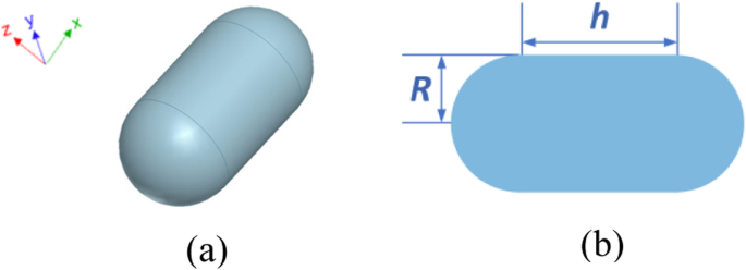
银纳米胶囊结构的配置。 一 3D 视图。 b 前视图和尺寸,其中 R =30 nm 和 h =60 nm
首先,我们改变入射光的波长λ 从 200 nm 到 400 nm 以模拟施加在纳米胶囊上的光学力。由于 FETI-DP 在频域中工作,因此在 15 个采样频率点计算光力。图 4 显示了施加在银纳米胶囊上的光学力的计算曲线。为了表明FETI-DP的准确性,将FETI-DP的光学力结果与商业软件Lumerical FDTD Solutions [33]的光学力结果进行比较,可以观察到良好的一致性。
<图片>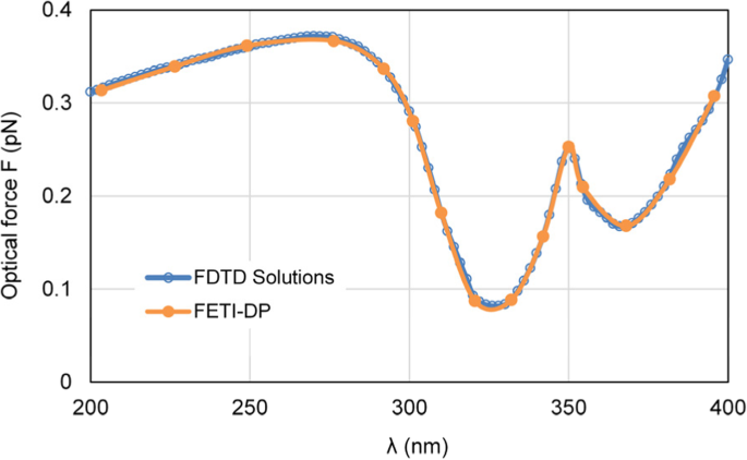
施加在银纳米胶囊上的光力结果随波长λ而变化 入射光,包括FETI-DP和商业软件FDTD解决方案的结果
Then, the performance of FETI-DP is tested for different numbers of subdomains. We increase the number of subdomains from 4 to 24 by keeping the discretization density. We assign each processor to deal with one subdomain. Table 1 reports the time used for the construction of global interface Eq. (6) and the total solution time. It can be seen that the FETI-DP can fully exploit parallel computing resources and significantly improve the solution efficiency. Besides, the accuracy of the FETI-DP with the number of subdomains increasing is also examined and reported in Table 1. Here, the accuracy is defined by the 2-norm relative error of the optical force as δ OF = ‖OF 我 − OF ref‖/‖OF ref‖, where OF 我 is the optical force using i subdomains and OF ref denotes the reference optical force using two subdomains. It can be seen that the accuracy keeps almost constant with the number of subdomains increasing.
Gold Nanosphere Dimer
The second example analyzes the optical trapping of a gold nanosphere by using a gold nanosphere dimer. The plasmonic effects at the dimer gap can effectively enhance the optical force for trapping nanoparticle. Figure 5 a and b gives the configuration and dimensions of this system. The constitutive parameters of gold are all measured values taken from [32]. The surrounding medium is water with a relative refractive index of n = 1.33. The incident light is a plane wave with the power of 10 mW/μm 2 , the electric field polarization direction is +x , and the incident direction is −z . The optical force exerted on the object nanosphere is calculated by the FETI-DP method. For the FETI-DP implementation, the whole computational domain is divided into 32 subdomains and discretized by tetrahedral meshes, which results in 3.5 × 10 6 unknowns, including 1.6 × 10 5 dual unknowns and 1738 corner unknowns.

Configuration of an optical trapping system of a gold nansphere dimer in water. 一 3D view. b Front view and dimensions, where R = 25 nm, r = 5 nm, and g = 2 nm
First, we test the parallel performance of the proposed FETI-DP by using various numbers of processors. Table 2 reports the solution time for Eq. (6) as well as the total solution time. Besides, the speedups for the parallel computation are also provided in Table 2. Here, the speedup is defined by
$$ \mathrm{Speed}\ \mathrm{up}=\raisebox{1ex}{${T}_1$}\!\left/ \!\raisebox{-1ex}{${T}_{N_p}$}\right. $$ (17)where \( {T}_{N_p} \) denotes the total wall-clock time using N p processors. It can be seen that the FETI-DP significantly improves the solution efficiency and exhibits good parallel speedup. For this large number of unknowns, the total memory usage of all the processors is only 57.2 GB.
Then, the effectiveness of the low-rank sparsification approach is examined. With the low-rank sparsification, the subdomain matrix can be factorized by data-sparse algorithm and stored as data-sparse matrices. The construction time and memory usage are only 18 s and 0.5 GB, while they are 67 s and 1.7 GB by conventional matrix algorithm. It can be seen that we get 72% time saving and 70% memory compression. Related to the memory usage, the subsequent MVPs can also get 70% time-saving.
Next, the FETI-DP is tested for the optical force calculation with the wavelength λ varying from 277 nm to 818 nm. In practice, the analyses of optical force under incident light of different wavelengths are often necessary for searching the plasmonic resonance wavelength, where drastic field enhancement occurs and the strongest optical force can be obtained. Two cases are considered with the nanosphere located at (0, 0, 20 nm) and (0, 0, − 20 nm). Figure 6 a and b plots the calculated optical forces exerted on the nanosphere for different λ . It can be seen that the maximum optical force occurs at λ = 472 nm, which is the plasmonic resonance wavelength. The optical force at this resonance wavelength enhanced by nearly 40 times as against that at non-resonance wavelength. Moreover, the optical force always points to the dimer gap, as shown in Fig. 6, where the electric field intensity is strongest. It is also the direction of gradient force to trap the object. Figure 7 a and b shows the calculated electric field enhancement distributions at the non-resonance wavelength of λ = 300 nm and the resonance wavelength of λ = 472 nm, respectively. It can be seen that the electric field intensity has been increased by almost 250 times due to the plasmonic resonance effect.

Calculated results of optical forces exerted on the nanosphere in the system of gold nanosphere dimer, varying with the wavelength λ of incident light. 一 The object nanosphere is located at (0, 0, 20 nm). b The object nanosphere is located at (0, 0, − 20 nm)

The electric field enhancement distributions on the xoz plane for the system of gold nanosphere dimer. 一 λ = 300 nm (non-resonance wavelength). b λ = 472 nm (resonance wavelength)
Besides, the optical force and optical potential are calculated with the nanosphere moving from (0, 0, − 30 nm) to (0, 0, − 17 nm) along the z -轴。 Since the most typical and interesting behavior of trapping forces and potentials are those acting along z -direction, we here consider the axial trapping potential by integration along the z -轴。 Because the motion of the nanoparticle is restricted to one dimension, the definition of an optical potential is unambiguous from (16), even though the total optical force from (15) is non-conservative. As shown in Fig. 8 a, b, with the nanosphere moving to the dimer gap, the optical force and optical potential depth obviously increase. At the position of (0, 0, − 17 nm), an optical potential depth of 4.6 k B T is produced, which is sufficient to overcome the Brownian motion in water to achieve stable optical trapping.

The optical forces and optical potentials exerted on the nanosphere in the system of gold nanosphere dimer, when the nanosphere moves from (0, 0, − 30 nm) to (0, 0, − 17 nm). 一 The optical forces. b The optical potentials
Finally, we test the effects of the dielectric substrate for this example. The optical forces are calculated with and without a substrate, respectively. For both two cases, the nanosphere is located at (0, 0, − 20 nm) and the incident wavelength is chosen as the resonance wavelength. For the case without substrate, the calculated result of the optical force is |F 0| = 0.769 pN. For the case with a substrate, the gold nanosphere dimer is put on a dielectric substrate with a thickness of 60 nm and a relative permittivity of ε r = 2.25. The calculated result of the optical force is |F 1| = 0.761 pN. The relative error between these two results of optical forces is about 1.0 × 10 −2 , which is defined as |F 1 − F 0|/|F 0|.
Gold Truncated Cone Dimer
The third example deals with the optical trapping of a gold nanosphere by using a gold truncated cone dimer. Figure 9 gives the configuration and dimensions of this system. The constitutive parameters of gold are taken from [32]. The dielectric substrate has a relative permittivity of ε r = 2.25. The surrounding medium is water with a relative refractive index of n = 1.33. The incident light is plane wave with the power of 10 mW/μm 2 , the electric field polarization direction is +x , and the incident direction is −z . The whole computational domain is divided into 32 subdomains and discretized by tetrahedral meshes, which leads to 3.1 × 10 6 unknowns, including 1.3 × 10 5 dual unknowns and 1227 corner unknowns.

Configuration of an optical trapping system of a gold truncated cone dimer based on a dielectric substrate in water. 一 3D view. b Front view and dimensions, where UR = 20 nm, LR = 30 nm, h = 35 nm, and g = 2 nm
First, we analyze the optical forces by changing λ from 277 nm to 818 nm. Figure 10 plots the calculated optical forces exerted on the nanosphere for different λ . The nanosphere is located at (0, 0, 35 nm). It can be seen that the maximum optical force occurs at λ = 464 nm, which is the plasmonic resonance wavelength, and the optical force here is enhanced by nearly 30 times at non-resonance wavelength. Moreover, the total optical force always points to −z , as shown in Fig. 10, which is the direction of the gradient force. This confirms that the gradient force is greater than the scattering force, which is one of the conditions that the nanosphere can be stably trapped. Figure 11 a and b presents the calculated electric field distributions at the non-resonance wavelength of λ =300 nm and the resonance wavelength of λ = 464 nm, respectively. It can be seen that electric field intensity has been increased by almost 500 times due to the localized surface plasmon resonance.

Calculated results of optical forces exerted on the nanosphere in the system of gold truncated cone dimer, varying with λ . The nanosphere is located at (0, 0, 35 nm)

The electric field enhancement distributions on the xoz plane for the system of gold truncated cone dimer. 一 λ =300 nm (non-resonance wavelength). b λ =464 nm (resonance wavelength)
Then, the location of the nanosphere is changed to 0, 5, and 35 nm to observe the optical force. Figure 12 gives the calculated optical forces exerted on the nanosphere, where obvious y -component of optical force can be observed, while greater z -component of optical force exists. The total optical force still points to the position with the strongest electric field to trap the nanosphere.

Calculated results of optical forces exerted on the nanosphere in the system of gold truncated cone dimer varying λ . The nanosphere is located at (0, 5 nm, 35 nm)
Furthermore, we analyze the optical potential with the nanosphere moving from (0, 0, 50 nm) to (0, 0, 20 nm) along the z -轴。 Here, we consider the axial trapping potential along z -direction, which restricts the motion of the nanoparticle to one dimension and leads to an unambiguous definition of optical potential. Both the optical force and potential are calculated. As can be observed from Fig. 13 a, b, with the nanosphere moving to the dimer gap, the optical force and the optical potential depth obviously increase. At (0, 0, 20 nm), an optical potential depth of 3.8 k B T is obtained, which is sufficient to overcome the Brownian motion in water to achieve stable optical trapping.

The optical forces and optical potentials exerted on the nanosphere in the system of gold truncated cone dimer, when the nanosphere moves from (0, 0, 50 nm) to (0, 0, 20 nm). 一 The optical forces. b The optical potentials
Finally, we test the computational costs of the FETI-DP by changing the number of unknowns from 1.0 million to 3.2 million based on different mesh size. In practice, the tests under different mesh density are usually necessary to meet different accuracy requirements. Such a large-scale complex problem brings great challenges to conventional numerical methods. However, the FETI-DP can easily handle this problem. Thirty-two processors are employed for the FETI-DP simulation, while each processor deals with a subdomain. Table 3 reports the computational costs of the FETI-DP. It can be seen that the FETI-DP exhibits high simulation efficiency and low memory requirement.
结论
An FETI-DP method combined with low-rank sparsification is proposed for the prediction and analysis of optical trapping of metal nanoparticles. The proposed method provides fully decoupled subdomain problems, which converts a large-scale complex problem into a series of small-scale simple problems. It is well-suited for parallel computation and can significantly improve the efficiency of numerical simulation. Examples demonstrate that the proposed method exhibits excellent performance of large-scale computation and is well-suited for the fast and accurate simulation of optical trapping at nanoscale.
数据和材料的可用性
本研究中生成或分析的所有数据均包含在本文中。
缩写
- ABC:
-
Absorbing boundary condition
- DOF:
-
Degrees of freedom
- FDTD:
-
有限差分时域
- 有限元:
-
有限元法
- FETI-DP:
-
Dual-primal finite element tearing and interconnecting
- MST:
-
Maxwell stress tensor
- MVP:
-
Matrix-vector product
纳米材料