

用于 Micro-LED 和 VCSEL 的高级原子层沉积技术
摘要
近年来,纳米器件的工艺要求导致半导体器件的规模逐渐缩小,随之而来的蚀刻引起的侧壁缺陷也不容忽视。由于等离子体增强化学气相沉积无法提供足够的阶梯覆盖,因此利用原子层沉积ALD技术的特性来解决这个问题。 ALD 利用前体气体和基板表面之间的自限性相互作用。当反应气体形成单层化学物质吸附在基板表面时,它们之间不会发生反应,生长厚度可以控制。在 Å 级别,它可以提供良好的阶梯覆盖。在这项研究中,回顾和比较了最近关于微发光二极管和垂直腔面发射激光器的 ALD 钝化的研究。几种钝化方法被证明可以提高光效率,减少泄漏,并提高可靠性。
介绍
原子层沉积 (ALD) 技术的发展始于 1970 年代。 1977年,芬兰的Tuomo Suntola博士正式申请了ALD技术的第一项专利[1]。 1983 年至 1998 年间,ALD 技术被应用于芬兰赫尔辛基机场的电子显示器生产。 1990年代后期,由于ALD工艺引入半导体行业,投入了大量的研发资金和人力,为ALD工艺技术的快速发展做出了重要贡献。 2007年,英特尔采用ALD工艺技术生长出二氧化铪(HfO2)栅极钝化层,应用于45纳米微处理器上的金属氧化物半场效应晶体管,进一步巩固了ALD工艺技术在半导体行业的重要性[2].
ALD基于表面化学反应[3],具有优异的原子级厚度精度、大面积高均匀性、薄膜在高纵横比结构上的一致性等特点。与传统的化学气相沉积 (CVD) 或物理气相沉积 (PVD) 不同,如图 1 所示,ALD 工艺通常使用两种不同的化学前体。它们在不同的时间进入反应室,形成两个半循环反应,所有的化学反应都通过化学吸附被限制在表面。这两个半循环反应构成了促进单层膜沉积的 ALD 循环,可以逐层重复以生长膜。这些表面化学反应发生在自限反应的条件下,这是 ALD 工艺窗口。采用两次半循环反应沉积薄膜,避免了反应室中同时存在两种化学前驱体,形成CVD等沉积模式,使ALD技术能够精确控制薄膜厚度和均匀性[4, 5,6,7]。
<图片>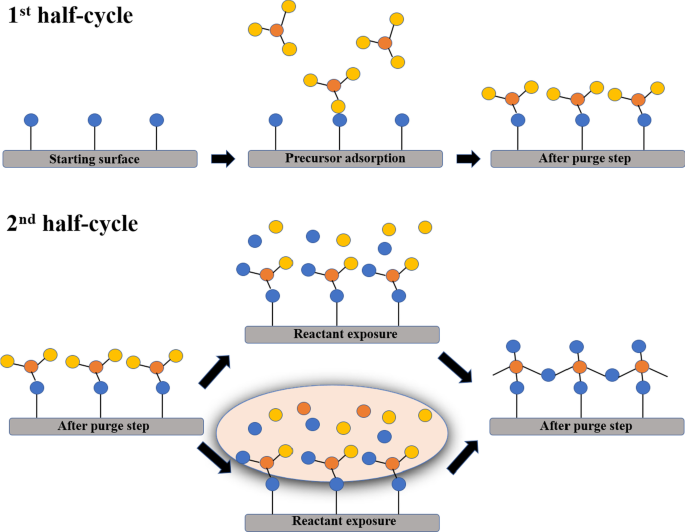
热和等离子体辅助ALD示意图
ALD 薄膜的生长速率由每周期生长 (GPC) [8, 9] 表示。一般而言,GPC 的厚度范围为 0.05 至 0.1 纳米。化学前体的选择会影响薄膜的质量、生长速度和工艺所需的时间。 ALD 沉积过程由四个连续步骤组成:脉冲 A、清洁 A、脉冲 B 和清洁 B。脉冲 A 由金属前体蒸气组成,脉冲 B 由非金属前体蒸气组成。在清洁A和清洁B期间,惰性气体例如氮气或氩气和真空泵用于从反应空间清洁气态反应副产物和残留反应物分子。沉积顺序包括至少一个沉积循环。重复沉积循环,直到沉积序列产生所需厚度的薄膜。
自限反应形成了 ALD 的核心 [10,11,12,13]。设置和调整工艺参数(如工艺温度、化学前驱体选择、用量等)使表面化学反应达到自限状态是 ALD 工艺发展的第一步。在满足ALD工艺窗口的情况下,所有化学反应都发生在表面,满足自限条件。因此,如果在每个 ALD 循环中引入足够的化学前体分子,则参与表面化学反应的化学前体的总量取决于表面反应基团的数量。如果将工艺温度控制在化学前体分子不在物理吸附和自动热裂解范围内的水平,则可以在每个 ALD 循环中在所有基板表面上均匀沉积原子层。因此,ALD技术具有优异的均匀性和保形能力,可以降低薄膜的厚度。控制精度是原子水平的关键因素[14,15,16,17]。
ALD最重要的应用是在半导体领域[18,19,20,21,22],例如制备高k电介质、金属薄膜、铜阻隔膜和鳍片领域的蚀刻停止层-效应晶体管 (FinFET) [23,24,25,26,27,28]、氧化物钝化层和 LED 和 VCSEL 的抗反射层。 ALD 非常均匀的覆盖范围和高密度薄膜特性使其适用于对水和氧气敏感的设备。因此,ALD已成为对可靠性要求高的器件保护层的最佳镀膜工具。水蒸气透过率(WVTR)是衡量薄膜对水和氧气的抵抗力的重要指标,尤其是对水蒸气敏感的柔性有机发光二极管(OLED)显示器[29,30,31, 32,33,34,35,36,37]。它的值需要达到 10 −4 克/米 2 -天或更少。对于其他大功率VCSEL、功率器件、高端LED,其WVTR至少需要小于10 -3 克/米 2 -day 以确保在恶劣环境中的可靠性。因此,这些器件已开始使用 ALD 钝化来确保其稳定性 [38,39,40,41,42,43,44]。除了上述应用之外,光伏[45,46,47]、锂电池[48,49,50]、燃料电池和微机电系统(MEMS)设备也使用了许多ALD工艺[6, 51, 52,53]。在本文中,我们重点关注 ALD 技术对器件性能的影响,并回顾了 VCSEL 的案例。此外,本文还概述了用于提高 VCSEL 性能的 ALD 工艺。
Micro-LED 的 ALD 技术
蓝绿光 LED 主要由 InGaN 基材料组成。由于其晶体结构,它是一种压电材料。它具有很强的内置电场,会影响有源区的发射波长和载流子复合效率。这种现象被称为量子限制斯塔克效应(QCSE),这是 LED 发光效率提高的主要原因之一 [54]。因此,研究团队通过绿色外延片上的环形纳米结构来利用 QCSE 的特性。该结构的制造释放了 LED 有源区的应力,以实现波长调制。它将发射波长从绿色调制到蓝色,因为纳米结构牺牲了部分发光区域并降低了发光强度 [55]。图 2 显示了微型 LED (μ-LED) 的示意图。随着μ-LED尺寸的减小,侧壁缺陷对晶圆的影响更大,导致芯片发光效率降低[56,57,58]。微型 LED 的钝化通常使用等离子体增强化学气相沉积 (PECVD) 来完成,它使用基于氢的前体来实现快速沉积速率 [30, 32]。 ALD 是微型 LED 的首选。与PECVD沉积的钝化层相比,ALD能够沉积纳米级厚度的高度致密的介电薄膜。 ALD 通过提供紧凑和致密的介电薄膜以及更好地控制薄膜厚度,为 μ-LED 的钝化提供了一种有前途的方法。因此,许多研究团队引入了ALD薄膜钝化保护技术来替代传统的PECVD方法。 F Koehler 等人。据报道,标准 PECVD 可以在中等温度 (400°C) 下沉积薄膜,但会受到强烈的负载影响。 ALD 的优点是在低温下具有良好的保形性。此外,ALD 显示出优异的晶圆间和晶圆内均匀性 [59,60,61]。此外,Milojevic [38] 报告说,较小的 μ-LED 中漏电流的增加可能是由于 PECVD 的介电质量。这种增加表明PECVD侧壁钝化不足以降低周长/面积比大的μ-LED的漏电流;中村等人。已经使用 ALD 和 PECVD 研究了侧壁钝化对 μicro-LED 的光电效应,这些结果还表明 ALD 更有利于增强光学和电学效应 [62]。 ALD钝化保护层具有高密度、高阶梯覆盖、有效的缺陷修复等特点,可以防止载流子被器件表面的缺陷捕获。因此,器件的发光强度大大增加,从而提高了效率[44, 55, 60, 63,64,65,66,67]。
<图片>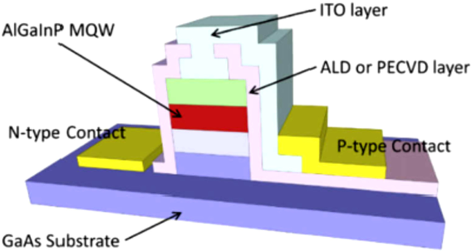
μ-LED 示意图 [67]
考虑到PECVD和ALD生长的钝化保护层对漏电流的影响,图3显示了PECVD和ALD钝化保护后红色μ-LED的漏电流图[66,67,68]。观察到使用 ALD 的器件的平均泄漏电流比使用 PECVD 获得的低得多。此外,由于小器件的表面积与体积比的增加和反向偏置下的额外泄漏路径,泄漏电流随着组件尺寸的减小而均匀增加。
<图片>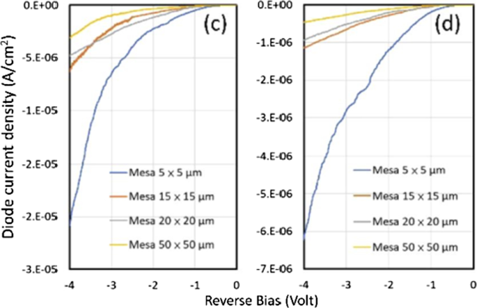
a 的反向偏置 J-V 曲线 PECVD 样品和b ALD 样品 [68]
为了说明钝化保护层对红光μ-LED光功率的影响,图4比较了不同尺寸和电流密度下PECVD和ALD钝化保护层的光功率。可以看出,当元件尺寸在 15 µm 以上时,PECVD 和 ALD 钝化层的光功率可以达到令人满意的水平,但当元件尺寸小于 5 µm 时,ALD 的性能优于 PECVD 提供的钝化保护。通过比较具有不同涂层和不同电流水平的设备,可以观察到集成光功率的急剧下降。在相同的电流密度和不同的尺寸下,ALD提供的光功率相差570倍,而使用PECVD的元件则高达850倍。这表明 ALD 仍然可以为小部件提供出色的钝化。保护层能够持续抑制表面缺陷并提高辐射复合效率。此外,ALD 提供的钝化保护提高了器件的可靠性。由于干蚀刻工艺会对侧壁造成损伤和缺陷,当器件尺寸减小时,侧壁缺陷的影响可能会成比例地增加,导致性能过早下降。因此,钝化层的质量尤为重要。上述结果表明,随着器件尺寸的缩小,ALD 钝化保护的器件在不同条件下表现更好。在未来的先进制造工艺中,ALD技术有望继续发挥重要作用。
<图片>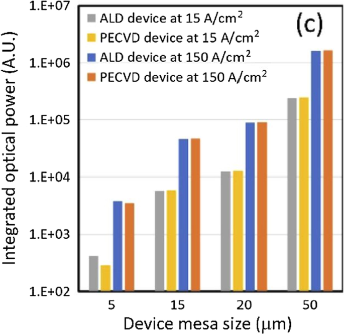
高/低电流密度下ALD和PECVD样品的积分光谱强度[68]
考虑到 EQE 的影响,本研究确定侧壁上存在钝化层,并比较了通过 ALD 和 PE-CVD 产生的钝化层对 EQE 的影响如下: LED-1:μ-LED 未经受到侧壁钝化; LED-2:经过ALD侧壁钝化和电感耦合等离子体蚀刻的μ-LED; LED-3:经过PE-CVD侧壁钝化和HF蚀刻的μ-LED; LED-4:经过 ALD 侧壁钝化和 HF 蚀刻的 μ-LED。图 5a、b 显示了 100 × 100 μm 2 获得的 EQE 和 20 × 20 μm 2 器件,分别说明不同侧壁钝化技术的影响。所有钝化的100 × 100 μm 2 μ-LED 具有类似的峰值 EQE(LED-1,40%;LED-2,36%;LED-3,38%;和 LED-4,41%)。由于周长面积比小,侧壁损伤对器件性能影响不大。因此,侧壁钝化不会显着影响大型 μ-LED。此外,在较大器件的情况下,EQE 受侧壁损坏的影响较小,并且不会随着侧壁钝化而改善。对于 100 × 100 μm 2 对于样品,无论使用何种侧壁钝化方法,EQE 下降都会发生变化,尽管最大 EQE 保持不变。对于面积为20 × 20 μm的μ-LED 2 ,使用和不使用 ALD 钝化实现的 EQE 分别为 33% 和 24%。这一结果归因于增强的光提取、表面重组和侧壁损伤导致的漏电流降低的综合作用。
<图片>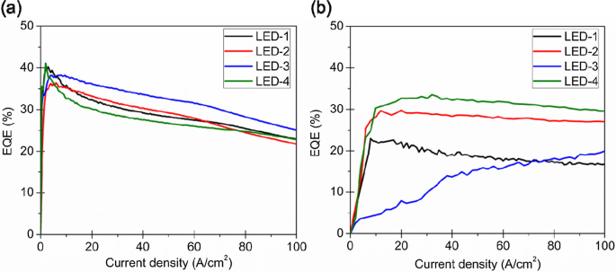
a 的 EQE 对电流的依赖性 100 × 100 μm 2 和 b 20 × 20 μm 2 不同侧壁钝化方法的器件[63]
因此,μ-LED 技术具有改变固态照明业务的巨大潜力,它肯定会成为改变游戏规则的显示技术。侧壁钝化对于保持高性能所需的可靠性以及进一步减小器件尺寸至关重要。一般来说,ALD 是进行侧壁钝化以防止 μ-LED 效率下降的关键技术,因为它们的特征尺寸因漏电流而减小到微米级 [69]。
用于 VCSEL 的 ALD 技术
氧化物 VCSEL 有许多优点,例如更好的模态稳定性和数据传输应用的低抖动,以及非密封收发器封装的低成本。然而,由于激光器的高功率密度,氧化物VCSEL也需要更多的保护措施来防止激光器特性的突变。
VCSEL 由三部分组成:顶部分布布拉格反射器 (p-DBR)、腔体和底部 n-DBR。 DBR 由 20-40 对薄膜组成。腔体通常为几微米厚。与侧发射极的增益长度相比,VCSEL的有源层的增益长度非常小(几十纳米)。为了获得辐射光的受激发射,DBR必须具有非常高的反射率才能发生辐射光的受激发射。为了改善VCSEL的特性,ALD已被应用于制备钝化层、DBR、多量子阱(MQW)甚至VCSEL的透明电极。
用于 VCSEL 钝化层的 ALD 技术
ALD 已被应用于增强量子点和 LCD 的可靠性 [31, 32, 70, 71],对于 VCSEL 的钝化层,ALD 均匀致密的涂层薄膜可以提高其可靠性。插入致密薄膜作为 VCSEL 的氧化物钝化层对于保护 VCSEL 的腔体非常重要。早些时候,保护膜通常使用 PECVD 进行电镀。然而,通常需要厚膜来保持薄膜的致密性,这会导致过大的应力并影响VCSEL的可靠性。 ALD技术可以沉积特性类似于VCSEL钝化层的Al2O3薄膜,均匀致密的涂层薄膜可以使保护芯片完全绝缘。因此,ALD已被用于替代PECVD,成为VCSEL钝化层的最佳涂层工艺。
氧化物 VCSEL 在 85/85(85°C 和 85% 相对湿度,RH)测试中的可靠性非常高,因为与 DBR 层相比,AlGaAs 的氧化层具有更高的铝浓度。较高的氧化铝孔径导致氧化物-半导体界面处的腐蚀分层。谢等人。表明,暴露在潮湿环境中的氧化物 VCSEL 的很大一部分发生了位错生长、严重开裂和孔径表面退化 [72]。赫里克等人。还观察到由于暴露于 85/85 室中的湿气而引起的类似故障 [73]。在过去的二十年里,许多研究人员和公司投入研究防止 VCSEL 元件因水分进入而引起的老化,并提出了广泛的保护性钝化膜和版图设计更改。例如,在 2004 年,安捷伦科技公司提出蚀刻孔并填充到聚合物中以防止水分暴露 [74]。 2006年Debraander提出了台面钝化膜针孔检测方法[75],而2014年TrueLight提出了SiON钝化膜[76]。在这里,我们仅举一些研究作为例子。本研究主要使用 ALD 生长的 Al2O3 薄膜,并与 PECVD 生长的 SiNx 形成复合堆叠的防潮钝化薄膜。我们设计了实验并进行了对比研究,以展示ALD层对85/85测试失败的改善,PECVD和ALD沉积的VCSEL结构的耐潮介电层分别表示为器件A和器件B .
图 6 显示了 VCSEL 的结构,包括 n 型 DBR、MQW 层、高铝含量 (~ 0.98) AlGaAs 氧化物孔径层和 p 型 DBR 层。以下描述与标签有关。氧化后仅在器件B的侧壁上通过ALD沉积防潮钝化层。
<图片>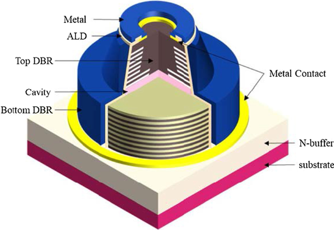
VCSEL示意图[42]
表 1 显示了本工作和其他组中 VCSEL 的比较。在这项工作中,研究了有和没有 ALD 的 VCSEL 的 LIV、S 21、眼图和湿高温工作寿命(WHTOL),这些结果表明 ALD 不影响高速度VCSEL,但提高了高速VCSEL的可靠性。
如图 7 所示,在预加重 NRZ-OOK 调制下,GI 单模光纤 (SMF) 中高达 100 米的 53 Gb/s 无差错传输是在少数几个直径为 6 微米的氧化物孔径的情况下获得的。 -模式 (FM) VCSEL。在这项工作中,ALD技术被用来提高FM VCSEL的可靠性。
<图片>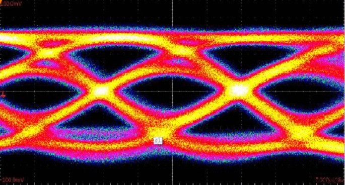
ALD 后 VCSEL 中氧化物孔径直径为 6 μm 的 53 Gb/s 无差错传输高达 100 m 的眼图
演示了设备 B 的直流、交流和传输性能。图 8a、b 显示了器件 B 在 25°C 时的光电流 (L-I) 曲线和小信号调制响应。图 9 描绘了 I 偏置下 56 Gb/s 的脉冲幅度调制 4 级 (PAM4) 眼图 =8 mA,25°C。图 10a、b 显示了 I 偏置下 28 Gb/s 的开关键控 (OOK) 眼图 =8 mA,设备 B 在 25°C 和 75°C 时。
<图片>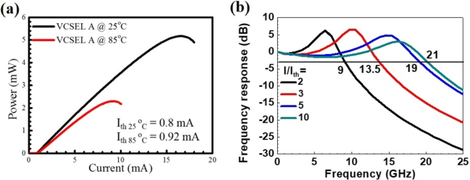
一 850 nm VCSEL 在 25°C 和 85°C 下的光电流特性,b 25°C 时器件 B 的小信号调制响应
<图片>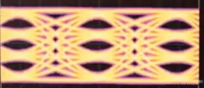
在 I 偏置下由 850 nm VCSEL 以 56 Gb/s 传输的 PAM4 信号的眼图 =8 mA,56 Gb/s,25 °C
<图片>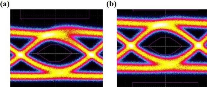
在 I 偏置下由 850 nm VCSEL 以 28 Gb/s 传输的 OOK 信号的眼图 =8 mA at a 25°C 和 b 75°C
为了研究通过钝化 Al2O3 ALD 层提高防潮性,定义了两个涂有介电层的器件。在器件 A 中,介电层仅涂覆了 SiNx,而在器件 B 中,它同时涂覆了 Al2O3 ALD 和 SiNx。 SiNx、聚酰亚胺、SiNx和金属化依次完成。第一个 p-金属与 GaAs 顶部材料形成欧姆接触。第二个p-金属是焊盘金属。复杂的堆叠钝化膜有效地覆盖了器件 B 中的台面表面。老化器件封装采用开罐式TO制备。
老化的环境条件为 85°C 和 85% RH,湿高温操作寿命 (WHTOL) 偏置为 6 mA。设备 A 和 B 的输入量分别为 18 和 18。结果如图 11 所示。在设备 A 中,有五个故障芯片,并且在 500 小时内随机发现故障。与设备 B 相比,直到 960 小时才发生故障。结果如图 11a、b 所示。这些结果表明,ALD 生长的 Al2O3 ALD 膜在台面侧壁上比仅 PECVD 生长的 SiNx 膜具有更好的密封性,以防止水分进入。
<图片>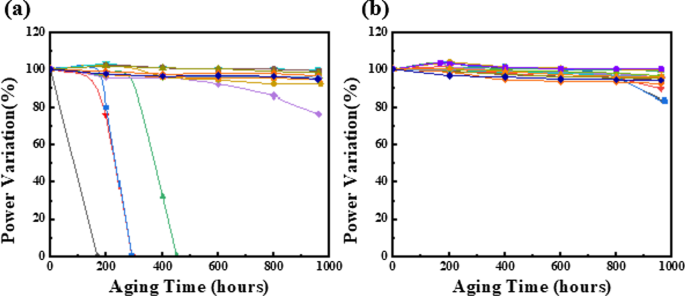
VCSEL 芯片的 WHTOL(85°C/85% 湿度)性能,a 器件 A,只有 SiNx 作为钝化层,b 器件 B,Al2O3/SiNx 作为钝化层
用于VCSEL DBR的ALD技术
ALD 沉积的 VCSEL 的 DBR 具有与蓝宝石衬底的良好粘附性和 DBR 不同介电层界面的良好条件 [80]。根据VCSEL的结构,激光垂直方向的腔由两组反射镜夹住有源层形成,光线在p-DBR和n-DBR之间经过多次反射后传播到空气中. DBR的结构由两种不同折射率的半导体材料组成,DBR的周期厚度应精确控制在λ/4(λ表示中心波长)。设计和生长方法构成了制造高反射率 DBR 的基础。对于高质量的 DBR,相位干涉效应有助于增强腔内的光,而 DBR 的高反射率(> 99%)可以大大提高 VCSEL 的阈值增益和量子效率。为了实现高反射率、宽阻带和温和的相位响应,DBR 的周期应在 20 到 40 之间,并且其制造材料应具有较大的折射率差异。在这种情况下,许多研究组报道了AIAs/GaAs、Al2O3、HfO2、SiO2等适合DBR的生长。
DBR 有多种生长方法,包括分子束外延 (MBE) 和金属有机气相沉积 (MOCVD)。但是,ALD 也是 DBR 的一种精确生长方法。由于ALD制备的低厚度、高反射率、低粗糙度的DBR可以有效改善VCSEL的性能,许多研究人员研究了使用ALD技术增强DBR的技术。例如,在 1997 年,Huffaker [81] 提出可以通过使用厚度小于四分之一波的 AlxO1-x 层来降低由于较低 DBR 引起的应变。 2013 年,郭等人。 [82]报道称,ALD工艺制成的DBR质量优于EBE工艺,ALD工艺时间与EBE工艺几乎相同甚至更少。此外,要生长至少由两种或多种材料组成的DBR,在EBE工艺中通常需要频繁地升高和降低温度,而在沉积不同材料的ALD工艺中可以保持温度相同。 2017 年,Liu [83] 报道称,ALD 方法可用于制备具有清晰界面和良好均匀性的高质量层。因此,ALD适用于沉积高质量的DBR。
例如,Sakai 等人。提出了在晶圆上制造具有 ALD 沉积 DBR 的蚀刻镜 UV-C 激光二极管(LD),这有助于降低激光阈值电流密度。在这项研究中,使用 ALD 为 DBR 沉积了四个周期的 HfO2 和 Al2O3。 Al2O3 被选为低折射率材料,因为它的沉积速率明显高于 SiO2。图 12 为 ALD 沉积 DBR 的 TEM 图像,显示了 DBR 优异的厚度和质量。
<图片>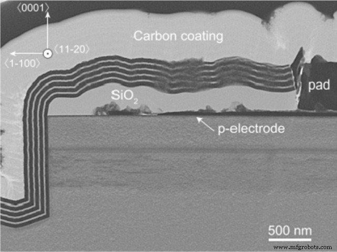
ALD沉积的DBR的TEM图像[84]
MOCVD技术在DBR的沉积中得到了广泛的应用,具有精确的薄膜生长控制和高质量薄膜沉积等诸多优点。但在实际生产过程中,DBR不同介质层的界面处界面状况会受到影响;否则,DBR 的设计方法将需要复杂的优化,例如在不同介电层的界面处沉积另一个额外的缓冲层。图 13a 显示了在没有插入缓冲层的情况下使用 MOCVD 计算 DBR 反射率的转移矩阵方法 (TMM)。用 ALD 沉积的 HfO2/Al2O3 DBR 的反射率光谱与图 13b 中计算的 TMM 光谱更一致 [85]。在这种情况下,与MOCVD相比,ALD技术可以沉积DBR,不同介电层之间具有更好的界面(图14)。
<图片>
用 a 沉积的设计 DBR 的测量和计算反射光谱 MOCVD,b ALD [84, 85]
<图片>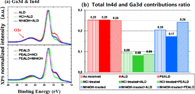
一 没有、有 HCl 或有 NH4OH 表面处理的 ALD 和 PEALD 样品的归一化 Ga3d-In4d 光谱的叠加,b 与 Al2O3 自由表面相比,相同样品的 Ga3d-In4d 比 [86]
用于 VCSEL 多量子阱的 ALD 技术
由于 VCSEL 对光学增益的高要求,大多数设备使用 MQW 作为有源区。一般来说,当MQW周期增加到一定值时,VCSEL的阈值电流密度主要由以下三个因素引起。首先,对于量子阱的宽度,有源区不能与波形的峰值位置重叠。量子阱离峰值位置越远,其增益效率越低。 Therefore, distant quantum well regions cannot play a significant role in improving the optical gain. Second, there is a direct proportional relationship between the total transmittance current and period of MQWs. The total transmittance current increases with the MQW period because the transmittance current is a part of the threshold current of the device. Therefore, the threshold current of the device will increase with the transmittance current. Third, as the current increases, the slope of the optical gain to current curve will decrease, increasing the threshold current of the device. Hence, thin MQWs with high crystalline quality and optical properties are promising candidates for realizing VCSELs.
For the MQWs of VCSEL, ALD can optimize the interface properties and surface recombination of MQWs [80, 83,84,85]. In the last several decades, methods for optimizing MQWs using ALD have been studied. In 2008, Lo et al. reported the successful growth of high-quality ultraviolet (UV) AlGaN/GaN MQWs structures using ALD [87]. In the same year, Bosund et al. [88] proposed that a thick TiN passivation layer deposited by ALD on top of InGaAs/GaAs can significantly increase the photoluminescence intensity and carrier lifetime of the MQWs, while Li et al. reported that a low dislocation density ultraviolet (UV) AlGaN/GaN MQW structure can be grown using the ALD technique. In 2019, Lee et al. [89] proposed that the emission intensity of the 860 nm GaAs VCSEL with SiN anti-reflection film was significantly increased (compared to the VCSEL without the SiN anti-reflection film) to improve the light extraction efficiency of a VCSEL. Here, we cite a few studies as examples.
A deep understanding of semiconductor–dielectric interface properties will provide guidelines for optimizing efficient passivation solutions for InGaN/GaN-based µ-LEDs. To this end, quantum well (QW) semiconductors are of tremendous interest because many surface recombinations are likely to occur at the edges of the LED active regions and are probably responsible for the low µ-LED efficiencies. Thus, Le Maoult et al. [86] studied the X-ray photoemission (XPS) and wavelength dispersive X-ray fluorescence (WDXRF) characteristics of In0.1Ga0.9N surfaces after acid, base, or sulfur-based chemical treatments followed by ALD of Al2O3 thin films with TMA/H2O or TMA/O2 plasma (plasma-enhanced ALD) at 250 °C.
The ALD of Al2O3 with H2O as a weak oxidizer does not seem to significantly modify the InGaN surface. Indium depletion occurs as the In4d intensity decreases, as observed previously in the case of the HCI or NH4OH-treated surfaces only (upper portion of Fig. 15a, b). On the contrary, during the PEALD of A12O3 (strong oxidizer), the NH4OH-treated surfaces changed compared to HCl because the In4d component level is indistinguishable from the PEALD reference (as illustrated by Fig. 15a, bottom, and 15b). Then, if indium is assumed to be the main species sensitive to plasma-induced oxidation, the indium-depleted surfaces after HCI treatment would indeed remain in a stable state of oxidation regardless of the ALD or PEALD process. On the contrary, a higher proportion of indium from the NH4OH-treated surfaces is more likely to be oxidized by the plasma species.

一 Superposition of normalized Ga3d-In4d spectra for ALD and PEALD samples without, with a 30’ (NH4)2S or with a NH4OH + 30’ (NH4)2S surface treatment, b proportion of O1s components and total indium contribution using In4d line [86]
If a 30' (NH4)2S surface treatment with or without prior treatment with NH4OH is performed before ALD, the quantitative analysis seems to report (Fig. 15b) results similar to those observed previously without the alumina layer. As an example, a similar decrease in the indium proportion was observed (~ 75%). However, a slight increase in the O–Al-related component from the O1s line was observed for the sample that underwent the double surface treatment, probably owing to the increased surface hydrolysis by the first NH4OH treatment. Thus, ALD does not seem to significantly modify the initial state of the (NH)S-treated surfaces. However, these results do not provide quantitative information regarding the proportion of sulfur after the deposition of Al2O3 by ALD. Considering that sulfur was adsorbed on InGaN before deposition, further investigations are required to determine the evolution of sulfur bonds after ALD of Al2O3, especially if binding state differences with stronger oxidizing processes such as PEALD are evident.
ALD Technologies for the Transparent Electrode of VCSEL
For the transparent electrode of VCSEL, ALD can deposit the electrode with high transparency and good current spreading properties [90]. In terms of the current spreading of the conventional VCSEL, the metal electrode has good current spreading properties, but strongly absorbs the emitted light. Hence, the conventional VCSEL relies on the upper heavily-doped layer for current spreading. However, since the upper heavily-doped layer has poor current spreading performance and absorbs part of the emitted light, the light output power of the device is lowered. Therefore, a transparent conductive oxide (TCO) film deposited by ALD, exhibiting excellent photoelectric performance, can solve the current spreading problem described above.
Figure 16 shows the SEM images of ZnO films deposited on Si with ALD and CVD modes as the transparent conductive materials, which can be applied to new-generation photovoltaic devices. So far, there are few studies and reports on the application of TCO films in VCSEL devices. At present, the indium tin oxide (ITO) films are used in VCSEL devices. In 1997, C. L. Chua et al. [91] first reported the top-emitted VCSEL with a transparent tin oxide electrode. In this study, the peak transmittance of ITO is 96%. In 2002, Jiang et al. [92] studied the P-type ohmic contact of ITO as an 850 nm GaAs-based oxide restricted type VCSEL. In comparison with VCSELs with traditional Ti/Au contact, they found output power of the VCSEL with ITO contact is 1.27 times higher than the VCSEL with T/Au contact. In 2014, Meng et al. [93] found that the output power of the 850 nm GaAs oxide-confined VCSEL with an ITO transparent conductive film is 1.18 times higher than the traditional VCSEL.

SEM images of ZnO films deposited on Si using ALD and CVD [90]
At present, the commonly used techniques for preparing TCO are magnetron sputtering, pulsed laser deposition, CVD, ALD, etc. However, it is difficult to achieve large-scale and large-area film formation using magnetron sputtering, the film deposited by pulsed laser deposition is uniform, and it is difficult to prepare large-area films while the deposition temperature for CVD is high, which renders it unsuitable for some devices that need to be prepared at low temperature. ALD possesses the advantage of highly controllable deposition parameters and the film deposited by it is characterized by good uniformity, absence of pinholes, and excellent shape preservation for film graphics. In this case, the oxide (TCO) film deposited by ALD can improve the properties of VCSELs.
Conclusions
This article reviews the application of ALD technology to the optoelectronic devices, µ-LEDs and VCSELs. Since sidewall damage is prominently observed in μ-LEDs when their sizes are reduced to the microscale level, this issue must be addressed to achieve high device performance. ALD sidewall passivation is a crucial technique because the sidewall damage can be reduced after passivating a surface with an ALD-grown dielectric. ALD passivation has also been found to help in protecting the quantum dot (QD) conversion layer in full-color displays. Different approaches involving the deposition of passivation layers have been established for reducing sidewall damage. In addition, an 85 °C/85% RH test with bias, which is a very difficult challenge for oxide-confined VCSEL devices, was conducted. In this study, we demonstrate that complex stacked dielectric layers as passivation films resist moisture ingress. The stacked passivation layers consist of Al2O3 growth by ALD film and SiNx growth by PECVD film. A very good encapsulation that prevented damage from moisture and excellent reliability was observed. In addition, the effects of ALD on the accurate control of DBR growth are specified. This technique has also been found to enhance the optical properties of MQWs, such as the deposition of an anti-reflection layer for improving the light extraction efficiency of a VCSEL and the accurate control of the growth of MQWs for improving its crystalline quality. In addition, because the output power of the VCSEL with an ITO transparent conductive film exceeds that of the traditional VCSEL, this study addresses the potential applications of ALD for preparing the TCO films of VCSELs.
Availability of data and materials
The data used and analyzed during the current study are available from the corresponding authors upon reasonable request.
缩写
- PECVD:
-
Plasma-enhanced chemical vapor deposition
- ALD:
-
Atomic layer deposition
- LED:
-
Light emitting diode
- VCSEL:
-
Vertical cavity surface emitting laser
- CVD:
-
Chemical vapor deposition
- PVD:
-
Physical vapor deposition
- GPC:
-
Growth per cycle
- HKMG:
-
High-K metal gate
- FinFET:
-
Fin field-effect transistor
- WVTR:
-
Water vapor transmission rate
- OLED:
-
Organic light-emitting diode
- MEMS:
-
Micro-electro mechanical systems
- μLED:
-
Micro-LED
- WHTOL:
-
Wet high-temperature operation life
- OOK:
-
On–off keying
- PAM4:
-
Amplitude modulation 4-level
纳米材料
- 三菱化学先进材料的目标是到 2023 年实现气候中和,到 2030 年实现正气候
- HfO2/TiO2/HfO2 三层结构 RRAM 器件在原子层沉积制备的 Pt 和 TiN 涂层衬底上的双极电阻开关特性
- 通过等离子体增强原子层沉积原位形成 SiO2 中间层的 HfO2/Ge 叠层的界面、电学和能带对准特性
- 通过原子层沉积和水热生长制备的抗菌聚酰胺 6-ZnO 分层纳米纤维
- 通过等离子体增强原子层沉积制备的 Co3O4 涂层 TiO2 粉末的光催化性能
- 通过超循环原子层沉积调节 ZnO 薄膜的费米能级
- CuGeO3 纳米线作为高级钠离子电池负极材料的合成和研究
- 在 c 面 GaN 上沉积的 AlN 原子层中界面和电特性的厚度依赖性
- 使用二氧化碳的低温等离子体增强原子层沉积 SiO2
- 用于计算机和电池的高级冷却系统
- 冷却液通道封闭的覆层和自由形式沉积
- 用于组件和组件的 SIGRABOND® 化学 CFRP