

硅烯中周期性电位下的自旋和谷值相关电子结构
摘要
我们研究了硅烯在周期性电位下的自旋和谷相关能带和输运特性,其中自旋和谷简并都被解除。发现狄拉克点、微带、带隙、各向异性速度和电导强烈依赖于自旋和谷指数。额外的狄拉克点随着电压电位的增加而出现,对于具有不同自旋和谷值的电子,其临界值是不同的。有趣的是,除了无间隙石墨烯之外,由于电场和交换场,速度被大大抑制了。对于特定谷附近的特定自旋,可以实现极好的准直效果。自旋和谷相关的带结构可用于调整传输,并在狄拉克点观察到完美的传输。因此,实现了显着的自旋和谷极化,可以通过结构参数进行有效切换。重要的是,周期势的无序极大地增强了自旋极化和谷极化。
背景
自从发现石墨烯(例如硅烯 [1, 2]、过渡金属二硫属化物 [3, 4] 和磷烯 [5])以来,具有六方晶格结构的二维 (2D) Dirac 材料得到了广泛的探索。尽管石墨烯具有许多特殊性质,但其应用受到零带隙和弱自旋轨道相互作用 (SOI) 的限制。最近,通过外延生长制造了石墨烯的硅类似物硅烯 [6-10],理论研究预测了其稳定性 [11, 12]。石墨烯和硅烯在 K 附近具有相似的能带结构 和 K ′ 谷,以及两者的低能谱由相对论狄拉克方程 [13] 描述。与石墨烯相反,硅烯具有很强的本征 SOI 和屈曲结构。强 SOI 可能会在狄拉克点 [13, 14] 处打开间隙,并导致自旋和谷自由度之间的耦合。屈曲结构允许我们通过垂直于硅片的外部电场控制带隙 [14-16]。此外,硅烯具有与现有硅基电子技术更兼容的优势。这些特性使硅烯成为下一代纳米电子学的优良材料。特别是在实验[17]中,通过生长-转移-制造工艺成功制备了室温下的硅烯场效应晶体管。
二维狄拉克材料的发现为探索谷的量子控制提供了新的机会。两个不等价的谷 K 和 K ′ 在第一布里渊区中可以被视为除了电荷和自旋之外的量子信息和量子计算的额外自由度 [18-20]。例如,可以合并谷自由度以将电子自旋量子位扩展为自旋谷量子位 [18]。因此,旨在产生、检测和操纵谷赝自旋的谷电子学引起了相当大的兴趣。在石墨烯中,通过利用独特的边缘模式 [21、22]、三角翘曲效应 [23]、拓扑线缺陷 [24、25]、应变 [26、27] 和静电门,已经提出了各种实现谷极化的方案[28]。与石墨烯相比,硅烯在谷赝自旋研究中具有显着优势。发现硅烯在不同外场的调制下表现出丰富多样的拓扑相和陈数[13,16,29,30]。存在电场E z 并交换字段 h , Ezawa 探索了 E 中的相图 z -h 以自旋和谷指数为特征的平面 [16]。进一步考虑 Rashba SOI,由于拓扑相变 [31],在硅烯中预测了谷极化量子反常霍尔态。基于状态转换,提出了一种具有近 100% 自旋极化的基于硅烯的自旋滤波器,它对弱无序具有鲁棒性 [32]。 Yokoyama 研究了通过铁磁 (FM) 硅烯结的弹道传输,并展示了可控的自旋和谷极化电流 [33]。在反转对称性被破坏的过渡金属二硫属化物中,由于时间反转对称性,由本征 SOI 引起的价带的自旋分裂在两个谷是相反的 [3, 34, 35]。破坏的反转对称性可能导致依赖于谷的光学选择规则,可用于选择性地激发 K 中的载流子 或 K ′ 分别通过右或左圆偏振光 [3, 34]。在实验中,谷极化信号已通过光学 [36, 37] 和传输 [38, 39] 测量进行探测。在受到对称破坏的栅极电场的双层石墨烯中观察到巨大的非局域霍尔效应,并且非局域信号持续到室温 [38]。参考文献中提供了最近对二维狄拉克材料中的谷电子学的评论。 [40].
超晶格是在半导体和二维材料中设计电子结构的有效方法 [41]。当石墨烯或硅烯被放置在金属基材的顶部时,纳米级的超晶格图案可以在实验中自然出现[42, 43]。由于手性性质,石墨烯中的超晶格可能导致各向异性费米速度 [44] 重整化并在光谱中产生新的狄拉克点 [45-47],这已在实验中观察到 [43, 48, 49]。在具有电场 E 的硅烯超晶格中 z 并交换字段 h ,自旋和谷简并都被解除。经证实,由超晶格引起的微带结构和微带隙取决于自旋和谷值 [50]。此外,硅烯超晶格可以增强自旋和谷极化[51]。就像石墨烯一样,硅烯超晶格中有望出现许多新颖的电子结构。然而,关于硅烯超晶格的工作很少[50, 51]。在本文中,我们详细讨论了一个互补的方面,即硅烯的自旋和谷相关能带结构和输运特性。我们发现自旋和谷指数对额外的狄拉克点和各向异性速度有不同的影响,这些影响可以通过结构参数进行调整。由于电场和交换场,速度被大大抑制。实现了显着的自旋和谷极化,这种极化可以通过无序大大增强。
本文的结构如下。在“方法”部分,我们介绍了理论形式和色散关系。 “结果和讨论”部分显示了带结构、自旋和谷极化传输的数值结果。最后,我们在“结论”部分进行总结。
方法
在单粒子近似中,狄拉克点附近的硅烯的电子结构服从有效狄拉克哈密顿量。所考虑的系统是由一系列局部势垒U形成的一维硅烯超晶格 , 交换字段 h , 和垂直电场 E z . U , h , 和 E z 只存在于势垒宽度 d 的势垒区域 b , 而 U =h =E z =0 在井宽 d 的井区 w ,如图 1 所示。具有 Kronig-Penney 类型的超晶格仅沿 x 变化 方向,一个单位的长度是d =d b +d w .类似的模型已经在参考文献中讨论过。 [51, 52],主要关注热电和电子传输,而不是这项工作中研究的能带结构和无序效应。实验上,U 可以由金属门和 h 产生 可以通过 FM 绝缘体 EuO [33] 的磁性邻近效应产生,该绝缘体周期性地沉积在硅烯层的顶部(见图 1)。电场E z 垂直于硅烯施加可以诱导交错的亚晶格电势Δ z =ℓ E z , 2ℓ A的垂直间距≈0.46Å 和 B 由于屈曲结构而导致两个亚晶格的位置 [16]。因此,电子态可以用哈密顿量来描述,
$$\begin{array}{@{}rcl@{}} H =\hbar v_{F} (k_{x} \tau_{x} - \eta k_{y} \tau_{y}) + \Delta_ {\eta \sigma} \tau_{z} + U_{\sigma}。 \end{array} $$ (1)
上图:硅烯超晶格示意图。硅烯顶部的 FM 绝缘体,如 EuO 和 EuS,会在硅烯中诱导交换场,如石墨烯 [53] 所提出的那样。 FM 绝缘体顶部的金属栅极局部控制费米能级。下:有外场和无外场的硅烯能谱示意图
Δ η σ =Δ z -η σ λ 所以 描述了不同自旋和谷指数的带隙,可以通过交错电位 Δ 控制 z 和 SOI λ 所以 . U σ =U -σ h 是不同自旋指数的有效势。 η =±1 表示 K 和 K ′ 山谷。 σ =±1 表示自旋向上和自旋向下状态。 v F 是费米速度。在硅烯中,内在和外在的Rashba效应很小,可以忽略不计[15]。
由于沿 y 的平移不变性 方向,横波矢量k 是 是守恒的。谷η的波函数 并旋转 σ 每个区域的形式为 Ψ (x ,y )=ψ (x )e iky 是 与
$$\begin{array}{@{}rcl@{}} \psi(x) =A \left(\begin{array}{cc} 1 \\ \frac{\hbar v_{F} k_{-} }{\epsilon_{\eta \sigma}} \end{array}\right) e^{i q_{\eta \sigma} x} + B \left(\begin{array}{cc} 1 \\ \frac {- \hbar v_{F} k_{+}}{\epsilon_{\eta \sigma}} \end{array}\right) e^{-i q_{\eta \sigma} x}。 \end{数组} $$ (2)在势垒区,ε η σ =ε b =(E -U σ )+Δ η σ 和 x 波矢的分量 \( q_{\eta \sigma } =q_{b} =\sqrt {(E - U_{\sigma })^{2} - \Delta ^{2}_{\eta \sigma } - (\hbar v_{F} k_{y})^{2}} / \hbar v_{F} \)。在井区,ε η σ =ε w =E -η σ λ 所以 和 \( q_{\eta \sigma } =q_{w} =\sqrt {E^{2} - \lambda _{SO}^{2} - (\hbar v_{F} k_{y})^{ 2}} / \hbar v_{F} \)。 k ±=q η σ ±i η k 是 .传输概率T η σ 可以使用传递矩阵技术计算。零温度下特定谷中特定自旋的归一化电导由
给出 $$\begin{array}{@{}rcl@{}} G_{\eta \sigma} (E) =\frac{1}{2} \int_{-\pi/2}^{\pi/2 } T_{\eta \sigma} (E,E\sin \theta) \cos \theta d \theta, \end{array} $$ (3)其中 θ 是相对于 x 的入射角 方向。自旋和谷分辨电导定义为 \(G_{\uparrow (\downarrow)} =\left (G_{K \uparrow (\downarrow)} + G_{K^{\prime } \uparrow (\downarrow) )} \right) / 2 \) 和 \(G_{K (K^{\prime })} =\left (G_{K (K^{\prime }) \uparrow } + G_{K (K^{ \prime }) \downarrow } \right) / 2\) 分别。然后,我们引入自旋极化P s 和谷极化P v :
$$\begin{array}{@{}rcl@{}} P_{s} =(G_{\uparrow} - G_{\downarrow}) / (G_{\uparrow} + G_{\downarrow}), \ end{array} $$ (4) $$\begin{array}{@{}rcl@{}} P_{v} =(G_{K} - G_{K^{\prime}}) / (G_{ K} + G_{K^{\prime}})。 \end{array} $$ (5)基于布洛赫定理和波函数的连续性条件,色散关系E (k x ) 对于 K 附近的自旋向上和自旋向下电子 和 K ′ 谷值可以计算,
$$ \begin{aligned} \cos(k_{x} d) &=\cos(q_{w} d_{w}) \cos(q_{b} d_{b}) \\&\quad- \frac {(\epsilon_{b} q_{w})^{2} + (\epsilon_{w} q_{b})^{2} + (\epsilon_{b} \!- \!\epsilon_{w}) ^{2} k^{2}_{y}}{2 \epsilon_{w} \epsilon_{b} q_{w} q_{b}} \sin(q_{w} d_{w}) \sin( q_{b} d_{b}), \end{aligned} $$ (6)和 k x 是布洛赫波数。为了简化计算,引入无量纲单位:\(E \rightarrow E d / \hbar v_{F}\), \(U \rightarrow U d / \hbar v_{F}\), \(\ lambda _{SO} \rightarrow \lambda _{SO} d / \hbar v_{F}\), \(\Delta _{z} \rightarrow \Delta _{z} d / \hbar v_{F}\) , \(h \rightarrow hd / \hbar v_{F}\), k 是 →k 是 d , k x →k x d , d w →d w /d , 和 d b →d b /d .请注意,在 Δ z =λ 所以 =h =0,方程(6) 被简化为在周期性电位中发现的无间隙石墨烯,其中自旋和谷值都退化 [44-47]。从方程。 (6),我们可以看到交换字段h 单独可以引起自旋分裂,而谷保持退化。然而,谷简并可以通过电场E解除 z 在 SOI λ 的帮助下 所以 .因此,交换场和电场的结合可以提升自旋和谷简并[16, 31-33],如图 1 所示。在所提出的系统中,在不同谷附近具有不同自旋的电子将呈现不同的带结构和运输特征。
结果和讨论
在本节中,我们将使用上述方程来计算硅烯超晶格中不同自旋和谷指数的能带结构和输运特性。下面假设障碍和井的宽度相同。井和势垒宽度不等的情况下的结果 (d b ≠d w ) 类似于无间隙石墨烯 [47]。部分参数设置为d b =d w =50 nm 和 λ 所以 =3.9 meV 在硅胶中,除非另有说明。我们将集中讨论费米能级附近的前两个微带(最低价和传导微带)。
自旋谷相关能带结构
一、势U的影响 图 2 描绘了微带上的情况。为了同时讨论能带的有间隙和无间隙情况,我们设置 Δ z =7.8 meV=2λ 所以 .在没有潜力的情况下 (U =0), K 附近的自旋电子 山谷 (K ↑ 电子)和靠近 K 的自旋向下电子 ′ 山谷 (K ′ ↓ 电子)是无间隙的(见图 2 (a1, a4)),而自旋向下的电子靠近 K 山谷 (K ↓ 电子)和 K 附近的自旋电子 ′ 山谷 (K ′ ↑ 电子)有很大的间隙(见图 2 (a2, a3))。自旋向上(或自旋向下)电子的微带从 E 向负(或正)能量范围移动 h =0 , 由于有效势 U σ =U -σ h . K的能带结构 ↑ (或 K ↓ ) 电子和 K ′ ↓ (或 K ′ ↑ ) 电子呈现相对于 E 的镜像对称性 =0,与方程一致。 (6).然而,这种镜像对称性在 U 的存在下被破坏 .可以观察到,如 U 增加,额外的狄拉克点出现,其数量同时增加。额外的狄拉克点可以通过其附近波函数的手性来证明 [46]。硅烯体系中狄拉克点的特征很大程度上依赖于自旋和谷自由度,如图 2 所示。例如,在 U =135 meV 在图 2 (d1–d4) 中 K ↑ , K ↓ , K ′ ↑ 和 K ′ ↓ 电子,狄拉克点的数量分别为 5、6、4 和 7。对于 U 的特定值 ,例如 U K =40.66 meV ↓ 电子(见图 2 (b2))和 U K =100.63 meV ′ ↑ 电子(见图 2 (c3)),可以在 k 处生成一个新的狄拉克点 是 =0,它将分裂成一对,远离 k 是 =0 点但始终保持 k x =0,作为 U 进一步增加。因此,K 的带隙 ↓ 和 K ′ ↑ 电子是闭合的(见图 2 (b2, c3)),并且有间隙的系统变得无间隙。为了找到U的临界值 , 我们设置 d b =d w 和 k x =0。类似于无间隙石墨烯中的规则[47],考虑到隐函数定理,可以得出结论,新狄拉克点处的纵波矢满足q b =q w 当
$$\begin{array}{@{}rcl@{}} E_{0} =\frac{(U - \sigma h)^{2} - \Delta_{z}^{2} + 2 \eta \ sigma \Delta_{z} \lambda_{SO}}{2(U - \sigma h)}。 \end{array} $$ (7) 能谱与 k 是 对于几个不同的潜在 U 值 . (a1–a4) U =0; (b1–b4) U =40.66 meV; (c1–c4) U =100.63 meV; (d1–d4) U =135.0 meV。参数的值为h =8.0 meV,Δ z =7.8 meV 和 k x =0
对于 K ↑ 和 K ′ ↓ 具有 η 的电子 σ =1,当Δ z =2λ 所以 , 方程(7) 可以减少到
$$\begin{array}{@{}rcl@{}} E_{0} =\frac{U - \sigma h}{2}。 \end{array} $$ (8)相应地,方程。 (6) 变成
$$ {}\cos^{2}(q_{w} d_{w}) - \frac{\left(\epsilon_{b}^{2} + \epsilon_{w}^{2}\right) q_ {w}^{2} + (\epsilon_{b} - \epsilon_{w})^{2} k^{2}_{y}}{2 \epsilon_{w} \epsilon_{b} q_{w }^{2}} \sin^{2}(q_{w} d_{w}) =1, $$ (9)当 \(\left (\epsilon _{b}^{2} + \epsilon _{w}^{2}\right) q_{w}^{2} + (\epsilon _{b} - \epsilon _{w})^{2} k^{2}_{y} =-2 \epsilon _{w} \epsilon _{b} q_{w}^{2}\) 或 q w d =2n π (n 是一个正整数)。基于方程。 (8), 我们有 ε b =-ε w ,所以只有当 k 是 K 0=0 ↑ 和 K ′ ↓ Δ 处的电子 z =2λ 所以 ,对应原始狄拉克点。 q的解 w d =2n π 有表格
$$\begin{array}{@{}rcl@{}} k_{y0} =\pm \frac{1}{d} \sqrt{\frac{\left(E_{0}^{2}-\ lambda_{SO}^{2}\right)d^{2}}{(\hbar v_{F})^{2}} - (2n\pi)^{2}}。 \end{array} $$ (10)当 \(\sqrt {E_{0}^{2}-\lambda _{SO}^{2}}d / 2\pi \hbar v_{F} \geq n\), k 是 0 是实数,新的狄拉克点将出现在 (E 0,k 是 0)。 U 的低值 , k 是 0为虚数,n无解 ,这意味着没有额外的狄拉克点。 Dirac 点仅出现在 U 的临界值之后 ,例如 U K =40.66 meV ↓ 图 2 (b2) 中的电子,对应于 n =1。根据方程。 (10)、狄拉克点数N D 可以获得。当Δ z =2λ 所以 ,
$$\begin{array}{@{}rcl@{}} N_{D} =2 \left[ \frac{\sqrt{E_{0}^{2}-\lambda_{SO}^{2}} d}{2\pi\hbar v_{F}} \right] + 1 \end{array} $$ (11)对于 K ↑ 和 K ′ ↓ 电子,而
$$\begin{array}{@{}rcl@{}} N_{D} =2 \left[ \frac{\sqrt{E_{0}^{2}-\lambda_{SO}^{2}} d}{2\pi\hbar v_{F}} \right] \end{array} $$ (12)对于 K ↓ 和 K ′ ↑ 电子,其中 [...] 表示整数部分。请注意,在 U 的临界值处 ,例如 U =40.66 meV 和 100.63 meV,狄拉克点数为N D =2n -1 对于 K ↓ 和 K ′ ↑ 电子(见图 2 (b2, c3))。
方程(7)和(10)表明狄拉克点的位置和数量可以通过电场E进行调整 z 并交换字段 h .图 3 展示了狄拉克点的数量 N D 作为 U 的函数 对于 E 的不同值 z 和 h .当Δ z 在图 3a 中 =7.8 meV,随着 U 的增加 , N D 对于 K ↑ 和 K ′ ↓ 电子以奇数的形式增加,与方程一致。 (11)。 N D 对于 K ↓ 和 K ′ ↑ 电子以偶数的形式增加,与方程一致。 (12),除了N D 处于临界值。图 3a 和 b 之间的比较表明 h 增加,自旋向下(或自旋向上)电子的临界值逐渐减少(或增加)。当Δ z =15 meV≠2λ 所以 在图 3c 中,N D 对于所有电子以偶数形式增加,除了 N D 处于临界值。显然,U 的临界值 具有不同自旋和谷的电子是不同的。 Dirac 点可以通过参数 U 的联合调制来控制 , E z , 和 h .
<图片>Dirac 点数 N D 与潜在的U . (a ) h =8.0 meV 和 Δ z =7.8 兆伏; (b ) h =20.0 meV 和 Δ z =7.8 兆伏; (c ) h =8.0 meV 和 Δ z =15.0 meV
潜在的U 和屏障宽度 d b 可用于调节带隙,如图 4 所示。K 的带隙 ↑ 和 K ′ ↓ 电子很小,而 K 的间隙 ↓ 和 K ′ ↑ 由于Δ,电子很大 η σ =Δ z -η σ λ 所以 .作为 U 增加,所有的小能带逐渐向高能量区域移动(见图 4a),并且所有的带隙都显示出带有 U 的阻尼振荡 (见图 4b)。当 U =σ h ,有效电位为零,间隙达到最大值。差距在 U 的临界值处关闭 ,由于新狄拉克点的出现。图 4c、d 描绘了小能带和带隙对势垒宽度的依赖性 d b 在 U =0。在没有外场 (d b =0),微能带保持退化,费米能级间隙为 2λ 所以 .随着d的出现 b ,小能带分裂,谷和自旋变为非退化。 K 的迷你乐队 ↑ (或 K ↓ ) 和 K ′ ↓ (或 K ′ ↑ ) 电子保持关于 E 的镜像对称 =0(见图 4c)。作为 d b 增加,K 的差距 ↓ 和 K ′ ↑ 电子逐渐展宽。 K 的差距 ↑ 和 K ′ ↓ 当 d 时电子减少到零 b 满足 d b /d w =λ 所以 /Δ z , 然后随着 d 增加 b (见图 4d)。随着d的进一步增加,间隙宽度趋于饱和 b .此外,miniband 的宽度缩小为 d b 由于本征态的耦合较少,因此增加(图中未显示)。电场对带隙的影响与前人的研究相似[50]。
<图片>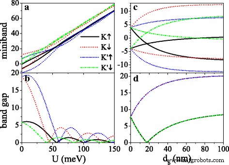
(a ) 费米能级附近的迷你带和 (b ) 他们在原始狄拉克点的带隙与潜在的 U , 在 d b =d w =50 纳米。 (c ) 费米能级附近的迷你带和 (d ) 他们在原始狄拉克点与 d 的带隙 b , 在 U =0 和 d w =50 纳米。其他参数的值为h =8.0 meV,Δ z =15.0 meV 和 k x =k 是 =0
群速度很大程度上取决于自旋和谷值指数,如图 5 所示。分量 (v x ,v 是 ) 的速度可以定义为
$$\begin{array}{@{}rcl@{}} v_{x} / v_{F} =\partial E / \partial k_{x}, \quad v_{y} / v_{F} =\部分 E / \部分 k_{y}。 \end{array} $$ (13) (a –d ) 速度与势 U , 参数设置为 h =20.0 meV 和 Δ z =7.8 meV。黑色、红色、蓝色和绿色实线是速度 v 0x , v 1x , v 2x , 和 v 3x , 分别。黑色、红色、蓝色和绿色虚线是速度 v 0y , v 1y , v 2y , 和 v 3年 , 分别
图 5 显示了速度分量 v mx 和 v 我的 以 v 为单位 F 在原始狄拉克点 (m =0) 和新的狄拉克点 (m =1,2,3)。人们可以将其视为 U 增加,v 0y 以衰减的方式振荡并且 v 0x ≈v F 几乎不受影响(见图 5a、d)。在 U 的临界值处 新狄拉克点出现的地方,v mx ≈v F 但是v 0y =v 我的 =0,表示沿 k 的准直行为 x 特定旋转和谷的方向。当 U 超过临界值并进一步增加,v 我的 增加到 v F 但是v mx 逐渐减少到零。由于手性性质,周期性电位的影响是高度各向异性的。由于间隙Δ,不同自旋和谷值的各向异性速度特征不同 η σ 和潜在的U σ , 可以通过使用 U 来命令 .以 U =20 meV 例如,v 0y =v F 对于 K ↑ 电子远大于 v 0y =0.16v F 对于 K ′ ↓ 电子,没有 v 0y 对于 K ↓ 和 K ′ ↑ 由于带隙的电子。 v mx (或 v 我的 ) 对于自旋向上的电子总是大于(或小于)同一谷中自旋向下的电子。值得注意的是,图 5 还意味着对于较小的 U , v 0x , v 0y , 和 v mx 小于 v F 由于Δ z 和 h ,除了无间隙系统[44]。例如,v 1x =0.98v F , 0.89v F , 0.89v F , 和 0.98v F 对于 K ↑ , K ↓ , K ′ ↑ 和 K ′ ↓ 当狄拉克点出现时,分别为电子。为了阐明Δ的影响 z 和 h 关于群速度,图 6 显示了速度 (v 0x ,v 0y ) 作为 (a) Δ 的函数 z (b) h 对于 K ↑ 电子。从图 6a 中我们可以清楚地看到 v 0x 随 Δ 单调递减 z 而 v 0y 对Δ的变化不敏感 z .相反,v 0x 对 h 不敏感 , 而 v 0y 增加到最大值 v 0y =v F 在 h =σ U 然后随着 h 减小 .结果表明Δ可以抑制群速度 z 和 h 硅胶。
<图片>速度 v 0x 和 v 0y 与 (a ) Δ z 和 (b ) h , 对于 K ↑ 电子。 (a ) h =20.0 meV 和 λ 所以 =Δ z /2。 (b ) Δ z =7.8 meV
自旋和谷地极化传输
自旋和谷相关的能带结构反映在输运性质上,并为控制输运提供了指导。在本节中,我们将讨论通过有限硅烯超晶格的自旋极化和谷极化传输的性质。图 7 显示了传输概率 T η σ 对于 (a, c) K ↑ 和 (b, d) K ↓ 电子和周期数 n =10。红色虚线是微带,它也是决定传输的不同电子状态的边界。我们可以看到传输受限于微带区域,而在带隙区域没有传输(见图 7a、b)。传输分布围绕 k 对称 是 =0 由于对称微带。传输的谐振特性源于谐振状态。需要注意的是,在k附近的gap区域仍然存在传输 是 =0 由于本征态的隧道效应。 T η σ K 的费米能级 ↑ 和 K ↓ 电子分别显示在图 7c、d) 中。可以清楚地看到许多带有 T 的薄共振峰 η σ =1 恰好出现在狄拉克点的位置,表明该系统可用作自旋谷滤波器。
<图片>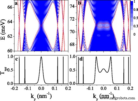
传输T的等值线图 η σ (E ,k 是 ) 对于 (a ), (c ) K ↑ 电子和 (b ), (d ) K ↓ 电子。参数值与图 2 (d1-d4) 中的相同,并且 n =10
能带结构对自旋和谷指数的强烈依赖性有利于实现高自旋和谷极化。图 8 显示了迷你带、电导 G η σ , 自旋极化 P s , 和谷极化 P v 作为潜在 U 的函数 . It can be found that the distribution of conductance is completely in agreement with the band structure, that is, the conductance (or conductance gap) corresponds to the miniband (or band gap). The minibands for spin-up and spin-down electrons could be alternative distribution by adjusting h 适当地。 Consequently, \(G_{K(K^{\prime })\uparrow }\) and \(G_{K(K^{\prime })\downarrow }\) present alternative distribution as well, i.e., \(G_{K(K^{\prime })\uparrow }\) nearly vanishes for those regions where \(G_{K(K^{\prime })\downarrow }\) is in resonance and vice versa. This result directly leads to a remarkable spin polarization, proposing a switching effect of spin polarization (see Fig. 8a). By changing Δ z , the minibands and conductances for electrons near K and K ′ valleys could be controlled, leading to a fully valley-polarized current (see Fig. 8b). Compared with spin polarization, the valley polarization is not perfect enough. However, this drawback could be remedied via the disorder structure of the system, as discussed in the following.

Minibands, conductances G η σ , spin polarization P s , and valley polarization P v versus potential U . (a ) Δ z =4.0 meV. (b ) Δ z =12.0 meV. Other parameters are set as h =7.0 meV, E =6.0 meV, d b =d w =120 nm, and n =10
Figure 9 shows the (a) spin polarization P s and (b) valley polarization P v in (U ,h ) space. Interestingly, both P s and P v present periodical changes in the considered region, which is not observed in the ferromagnetic silicene junction [33]. Both distributions of P s and P v are antisymmetric with respect to h →−h . It is possible to achieve independently a full spin and valley polarization by a proper tuning of the fields U and h . For example, when h =6 meV and U =42 meV, P s ≈1 and P v ≈1, meaning that the current is mainly contributed by K ↑ 电子。 When h =6 meV and U =44 meV, P s ≈1 and P v ≈−1 while P s ≈−1 and P v ≈−1 at h =6 meV and U =46 meV. The results demonstrate that a spin and valley polarization can be switched effectively.

Contour plot of (a ) spin polarization P s (U ,h ) 和 (b ) valley polarization P v (U ,h ), at Δ z =10.0 meV. The values of other parameters are the same as these in Fig. 8
In experiment, the structural imperfection of the model is unavoidable due to the limitations of the experimental techniques. Therefore, it is necessary to discuss the effect of the disorder on transmission. When the electric field or exchange field presents disorder, the conductance, spin polarization, and valley polarization are shown in Figs. 10 and 11. We set disorder situations of Δ z and h fluctuate around their mean values, given by 〈Δ z 〉=Δ z 0 and 〈h 〉=h 0,分别。 The fluctuations are given by
$$\begin{array}{@{}rcl@{}} \Delta_{z} |_{i} =\Delta_{z0} (1 + \delta \zeta_{i}), \quad h |_{i} =h_{0} (1 + \delta \zeta_{i}), \end{array} $$ (14)
Conductances (a ) G ↑ and (b ) G ↓ versus potential U , when the electric field presents disorder, at n =50 and Δ z 0=20.0 meV. The solid, dashed, dotted, and dash-dotted curves correspond to the disorder strength δ =0.0, 0.1, 0.3, and 0.6, respectively. The values of other parameters are the same as these in Fig. 8

Polarizations P s and P v versus potential U when a the electric field or b the exchange field presents disorder. Δ z 0=20.0 meV and h =7.0 meV in (a )。 Δ z =20.0 meV and h 0=7.0 meV in (b )。 The values of other parameters are the same as these in Fig. 10
where {ζ 我 } is a set of uncorrelated random variables or white noise, − 1<ζ 我 <1, δ is the disorder strength, and i is the site index. Note that the disorder only takes place in the x direction, and the system is always homogeneous in y 方向。 Thus, k 是 still keeps conservation. Figure 10 exhibits the effect of the disorder of the electric field on the conductances (a) G ↑ and (b) G ↓ . With the presence and increase of the disorder strength δ , both G ↑ and G ↓ are suppressed gradually, and each resonant peak splits into many small peaks. One may find that the conductance range is narrowed while the conductance gap range is broadened. Hence, the allowable (or forbidden) ranges of G ↑ completely fall into the forbidden (or allowable) ranges of G ↓ , giving rise to an excellent spin polarization (see Fig. 11). Furthermore, the positions of conductances and conductance gaps are nearly invariable as δ changes, suggesting that the miniband and band gap are insensitive to the disorder. Note that the disorder effect of the electric field on G K and G K ′ is similar to that observed in Fig. 10. Figure 11 presents the disorder effects of (a) the electric field and (b) the exchange field on polarizations P s and P v . Obviously, with the increase of δ , P s and P v increase greatly, and the polarization platform is broadened. Thus, a full spin and valley polarization is realized. Comparison between Fig. 11a and b indicates that the disorder effect of exchange field is more prominent. The results demonstrate that the disorder could enhance the spin and valley polarizations compared with the order case, which is an advantage in realistic application.
结论
In summary, we demonstrated detailedly that band structure and transport property of silicene under a periodic field strongly depend on the spin and valley degrees of freedom. The numerical results indicate that electrons with different spins and valleys have various characteristics in Dirac point, bang gap, and group velocity. In particular, owing to the electric field and exchange field, the anisotropic velocity is restrained, which displays a collimation behavior for specific spins and valleys. Therefore, the transmission presents strong spin- and valley-dependent feature, consistent with the band structure, resulting in a significant spin and valley polarizations. In addition, the disorder could greatly enhance the spin and valley polarizations. Finally, we hope these results can be conducive to the potential applications of the spin and valley indices.
缩写
- 2D:
-
二维
- FM:
-
Ferromagnetic
- SOI:
-
Spin-orbit interaction
纳米材料