

5 nm 爆炸纳米金刚石中 NV− 中心的光致发光:识别和对磁场的高灵敏度
摘要
氮空位含量(NV − ) 含氮炸药爆炸过程中产生的纳米金刚石 (DND) 的色心为 1.1 ± 0.3 ppm。对于尺寸 <10 nm 且具有有意创造的 NV − 的纳米金刚石,该值令人印象深刻 中心。从电子顺磁共振估计浓度,由 g 的积分强度确定 =4.27 线。这条线与“禁止”Δm有关 NV − 的塞曼能级之间的 s =2 跃迁 中心的地面三重态。共聚焦荧光显微镜能够检测 NV − 的红色光致发光 (PL) 由 5 纳米纳米粒子形成的纳米级 DND 聚集体中的色心。由 NV − 组成的亚波长发射器 比衍射极限光斑小几倍的尺寸被清楚地区分。我们进一步观察到,当 NV − 中基态和激发态自旋能级混合和反交叉时,PL 强度突然下降 发生在外加磁场下。这种效应是 NV − 的独特量子特性 中心,这是钻石晶格中其他可见域发光色心无法观察到的。
背景
含有氮空位的荧光纳米金刚石 (NDs) (NV − ) 中心是新型纳米材料,为创新应用开辟了道路。目前的具体应用包括磁传感 [1]、生物成像 [2] 以及电信和信息处理,包括使用纳米谐振器耦合光子源 [3、4]。 NV − 前所未有的独特量子特性产生了广泛的应用领域 色心出现在室温下。色心具有三重态自旋特性,可以通过光学可检测磁共振 (ODMR) [5] 检测到。纳米金刚石的荧光特性与其小尺寸 (<40 nm) 相结合,使其可用于生物医学应用,包括亚微米细胞器的细胞内对比成像和胚胎中的纳米级温度测量 [6,7,8]。将纳米金刚石微晶封装在生物相容的半透明壳中尤其有利于它们在生物环境中的应用 [9]。它们还可以用作点状探针,用于测量金属中的约翰逊噪声 [10]。纳米金刚石可以在炸药的爆炸过程中产生,即所谓的爆炸纳米金刚石 (DNDs)。然而,DND 通常包含高浓度的缺陷。例如,这限制了 DND(尺寸 <6 nm)在磁传感应用和其他纳米级局部探测中的应用 [11]。
DND 是由炸药在爆炸过程中释放能量的成分的热解产物合成的。爆炸物和爆炸物包含在水库中。合成发生在例如 13-20 μs 的时间段内,爆炸物块的大小最大为 10 cm。这个时间是爆炸波传播通过整个炸药块所需的时间。然而,每个单独的炸药微粒在更短的时间内分解和气化(<0.1 μs)。碳和氮是爆炸性物质的主要成分。在爆炸过程中,尺寸不超过 5 nm 的金刚石微晶是由爆炸成分的分解产物(主要是碳)自组装而成的。在合成过程中,氮也结合到金刚石晶格中。气相分解产物中 CH3* 自由基的存在导致复杂的 C-N-O-H 气体环境中的金刚石-晶格快速组装。气体环境在微秒级发生变化,快速卸压和温度下降提供了对应于金刚石合成所需区域的环境条件和碳的 Р-Т 相图上的稳定性 [12]。
金刚石微晶在凝聚中心(以及非金刚石形式的无定形碳)的极其快速的组装导致在生长的晶格内出现大量先验不同形态的缺陷、空位和多空位。由于在金刚石晶格快速组装过程中出现的堆垛层错和不准确,自然会出现空位。在温度降低的过程中,从爆炸期间的最大值下降到 800-900 °C,空位仍然可以在晶格内移动。因此,空位可以结合成簇或在微晶表面消失。在合成的这个阶段,空位的移动性也允许它们被取代的氮原子捕获。相同的过程也适用于氮杂质,唯一的区别是孤立的氮取代在低于 1600 °C 的温度下在晶格中实际上是固定的,因此仅在高温下聚集。氮杂质可以不同形式存在于 DND 的晶格中。它可以以高达 ~ 2.5 at.% 的聚合形式(A 中心、二聚体)或以孤立的碳取代原子(C 中心)的形式存在。众所周知,A 中心是非顺磁性的并且自旋为零,而具有自旋一半的 C 中心是中性形式的顺磁性(P1 中心)。因此,可以通过电子顺磁共振 (EPR) 方法轻松检测 P1 中心。晶格中的空位,带负电 (V − ),也是顺磁性的,但自旋为 3/2。在 DND 中发现了大量自旋半自旋 [13]。 EPR方法检测到的自旋半自由基的浓度几乎相同(1100-1400 ppm) 脚注1 在工业生产的所有标准 DND 中。这与具体的商业生产商及其技术细节无关,它们在更精细的细节上可能有所不同。自旋半自由基浓度大约是与粒子重量(或其中的相应碳原子数)相比,DND 粒子内置换氮原子和其他具有悬空键自旋的缺陷的总数之和。 DND 中的大部分氮(高达 ~ 2.5 at.%)或多或少均匀地分布在金刚石核心的共价晶格中,但在缺陷区域(如堆垛层错)中富集 [14, 15]。 Turner 等人也得出了结论。嵌入的氮主要以 N-N 二聚体(A 中心)或孤立的中性、带正电或带负电的氮 sp 的形式存在于金刚石晶格中 3 - 配位杂质(C 中心)[14, 15]。因此,DND中的大部分氮是位于金刚石晶格相邻节点的氮对(N-N)的非顺磁性形式。
除了普遍存在的氮杂质外,DND 颗粒还包含孤立的空位、多空位、氮空位氮 (NVN) 和氮空位 (NV) 型缺陷中心。这些额外的缺陷中心的出现是由于在晶格组装过程中相邻晶格位置中的成分自发出现 [11]。同时,带负电的NV − 的存在 位点主要是由于它们充电并接受来自过量中性氮原子的负电荷,在系统中扮演电子供体的角色。根据我们初步的 EPR 数据,NV − 可以从带有 g 的 EPR 线的积分强度确定的中心 - 半磁场中 4.26–4.27 的因子比孤立置换氮的浓度小约 2.5–3 个数量级,得出的值为 400–700 ppm。
多职位空缺和 NV − 在我们之前最近的工作中,通过 EPR 方法在 DND 中成功识别了中心 [13, 16, 17]。也已努力了解NV - 亮度之间的关系 DND 的中心及其表面的化学成分、环境和聚集体的形态 [18, 19]。控制 NV − 的发射特性的类似工作 还对具有人工创建的 NV 中心的合成荧光钻石进行了研究 [20]。然而,结合不同分析方法的必要研究,包括 X 射线粉末衍射、EPR 光谱、共焦荧光光谱和显微镜、元素分析、衍射极限尺寸的发射体分析以及磁场对光致发光信号的影响尚未完全进行关于NV − 的话题 除了我们的初步工作 [21]。目前,NV − 的发射特性的依赖性 在 DND 中对内部杂质含量和颗粒形态的影响尚不清楚。在这项工作中,我们报告了 DND 粒子表现出 NV − 的特定光致发光 (PL) 中心,精确计算 NV − 的内容 通过复杂的方法在它们中分析它们在光谱最大值处的 PL 强度作为金刚石微晶尺寸和氮含量的函数。此外,我们证明了 DND 对外部磁场的敏感性,这与其 ODMR 特性有关。
实验
制造方法和控制 DND 形态
DND 粉末是通过基本标准的过程获得的,该过程包括在几立方米的密闭不锈钢容器中对大约 1 kg 的三硝基甲苯-己原爆炸性混合物进行爆破,该混合物被适当厚度的水壳包围。这就是所谓的“湿”合成。产品的合成和初级纯化由商业制造商——俄罗斯圣彼得堡的特殊设计和技术局“SCTB Technolog”进行。该企业使用的技术工艺使得获得仅由纳米微晶组成的 DND 粉末成为可能,其相干散射区 (CSR) 的大小在 4.5 nm 到约 5.7 nm 的范围内变化。一些通过标准技术制备的纯化 DND 粉末由 PlasmaChem GmbH (Berlin, Germany) 提供。通过 X 射线衍射 (XRD) 确定交付的 DND 样品的形态。 XRD 谱是在法政大学微纳米技术研究中心(日本东京)通过配备 D/teX Ultra 探测器的 Rigaku SmartLab I X 射线衍射仪、CuKα 辐射源(λ =1.54178 Å) 和镍过滤器在角度范围 2θ =5–100 o (步骤 0.01 o )。分析过程中考虑了硬件功能的宽度。 X 射线 CSR 大小是根据 111、220 和 311 反射的宽度作为 2θ 角的函数的复杂分析的基础上确定的,根据参考文献中描述的方法。 [22]. 脚注 2 该方法的主要特点是晶格常数参数 (a o =3.5640 Å) 可用于所有 DND 样本,其系统误差(因选择不同模型而产生的差异)不大于 ± 0.0003 Å。 X 射线粉末衍射测量表明,为后续研究选择的一个代表性 DND 样品的 CSR 尺寸为 5.2 ± 0.2 nm。该 DND 样本用于下文所述的所有主要研究。此外,由同一制造商在特殊条件下(在引爆区有和没有无机添加剂)和具有不同 X 射线 CSR 尺寸的几个 DND 样品用于绘制光致发光强度与 CSR 尺寸的依赖性或/和内部氮的含量。普通工艺合成的DND粉体CSR粒径为4.6 ± 0.2 nm。
DND 粉末在沸腾的酸混合物中进一步纯化,以去除 3d 铁磁金属的任何残留杂质,从而允许更准确的 EPR 和 XPS 研究。拉曼散射和随后的光致发光研究需要通过在空气中将 DND 粉末在 430 °C 下退火 10-12 小时来进行额外的表面清洁 [23]。在酸纯化和在空气中处理之后,没有进一步努力去解聚含有单个离散纳米金刚石颗粒和尺寸低于 25 nm 的聚集体的 DND 粉末。水悬浮液中DND聚集体的平均粒径为25-30 nm。
用于共聚焦荧光显微镜研究的样品由 DND 的水悬浮液制成。通过将酸纯化和空气退火的粉末以 ≈ 1 mg/ml 的浓度分散在水中获得悬浮液,随后在水中稀释 100 倍。然后将 DND 悬浮液进一步旋涂到 170-μm - 厚盖玻璃基板,在超声波浴中在乙醇和丙酮的混合物中预清洗。最后,沉积在覆盖玻璃基板上的 DND 聚集体用 UV/O-Cleaner(低压汞灯:光功率> 25 mW/cm 2 在 λ =254 nm)约 30 分钟。在紫外光照射下,吸光sp的高效氧化和气相蚀刻 2 - 碳与氧气和臭氧发生在 DNDs 周围。 sp 的外部纳米级簇 2 -碳对于研究来自 DND 金刚石晶格中固有色心的 PL 是非常不理想的。将基材暴露于紫外线辐射还可以去除任何不需要的有机污染物,否则这些污染物会在宽光谱范围内产生发光背景。
表征方法
磁共振光谱
使用 EPR 光谱仪(JEOL JES-FA 300(日本))在室温下,在微波 X 波段内以~ 9.4393 GHz 或~ 9.0785 GHz 的频率记录样品的 EPR 光谱。使用的特定固定频率取决于整个研究周期中微波腔中石英绝热低温恒温器的存在与否。将数十毫克 DND 粉末引入外径为 5 mm 和 100 mm 石英底侧的长 X 波段 JEOL EPR 管(JEOL 零件目录,项目 4220 00281,编号 193)中。管子的开口顶部密封防潮。 JEOL EPR 管中和微波腔中心的 DND 粉末的照片如图 1a 和 b 所示。在两个面板中都清楚地看到灰色粉末。这样的DND粉量既适用于高Q因子EPR光谱仪的有效调谐,又适用于记录半磁场区弱信号光谱时获得良好的信噪比。
<图片>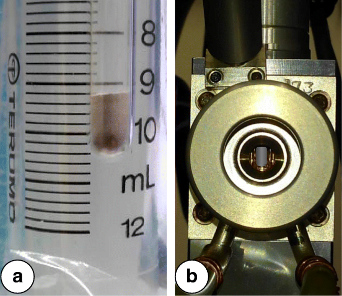
a中DND粉末的照片 JEOL EPR 管和 b 在 X 波段微波腔的中心。为了对比,EPR管中粉末的图像是专门针对一个体积为10 ml的塑料注射器的主体拍摄的
DND 的 EPR 光谱,具有 g - 4.00-4.30 范围内的信号因子,用微波功率记录,P MW =6 mW;磁场调制幅度,A m =0.5 mT;频率,ν =100 kHz;增益,G =1200;和信号积累,N =20。时间常数为 0.030 s。一次磁场扫描的记录时间为120 s。
扫描的最小和最大磁场值是用 JEOL-JES 程序软件专门选择的,并用 JEOL NMR 场计 ES-FC5(Echo Electronics)精确定义。 NV − 的浓度 通过将相应的 EPR 信号与 g 进行双重积分来估计中心 =4.27,然后分配给相应的样品重量并与参考样品的 EPR 信号进行比较。我们特意选择了合成荧光 Ib HPHT 金刚石粉 脚注 3 (平均尺寸 ~ 100 nm)具有明确定义的 g 积分强度 =4.27 EPR 线和已知的 S 浓度 =1 NV − 5.3 ± 0.4 ppm 的中心作为独立、可靠的参考,能够正确确定所获得的 NV − 浓度 在免打扰中。这类似于 Shames 等人先前提出的方法。 [24]。 g =4.27 EPR 线记录了该参考样品具有以下参数:P MW =3 μW,A m =0.2 mT,G =500,并且 N =12 在线性模式中,EPR 线的峰峰值强度与样品空间中微波功率的平方根成正比。对于亚微米和微米尺寸的 Ib HPHT 晶体,这种机制通常在低微波功率(低于 7-10 μW)下得到很好的实施。光谱是在 119 到 321 mT 的大范围磁场中专门记录的。该范围用于记录来自 Δm 的额外 EPR 信号 s =1 转换,允许低场,并代表 NV − 的独特签名 中心。
X 射线光电子能谱
使用配备单色 Al Kα 辐射源的 Perkin-Elmer PHI 5600 Multi-Technique 系统对 DND 进行 X 射线光电子能谱 (XPS)。分析~ 1 mm 2 样品区域发射的光电子通量,得到光电子的光谱特性 [25]。检测到的光电子从材料表面发射——几个原子层厚的区域 (<2 nm)。特别注意对碳 C1s、氮 N1s 和氧 O1s 的光发射峰面积的分析。通过一组适当的单线态轮廓将光电发射峰分解为单个成分。在用氩离子蚀刻表面后获取 DND 样品的光谱。在3 kV的加速电压和大约4 μA的离子束电流下进行离子蚀刻3 分钟。 Ar离子蚀刻用于从样品表面去除吸附的环境气体和其他化学吸附的原子复合物。 XPS还用于评估具有不同X射线CSR尺寸的一系列不同DND样品的内部氮含量。
荧光光谱
对于 PL 研究,通过将粉末齐平地压入直径为 2 mm 的浅孔中来制备样品,该浅孔在 4 毫米铜板上制成,然后用玻璃板平整表面。 PL 光谱通过定制的微拉曼装置记录在 540-1000 nm 范围内,使用 532-nm 激光激发,功率为 ~ 0.5 mW,衍射光栅每毫米有 600 个凹槽。曝光时间为180 s。激发辐射通过 Nikon Plan Apo 100x, NA =1.40 显微镜物镜聚焦在平坦的样品表面,形成直径为 2 μm 的光斑。光谱分辨率优于0.05 nm。
共聚焦荧光显微镜
为了注册 PL 光谱并映射来自旋涂在盖玻片上的 DND 粒子的 PL 信号,我们使用了进一步的 PL 设置。它由一个定制的倒置共焦扫描显微镜和一个成像光谱仪组成。共聚焦显微镜包括压电扫描台(NanoPDQ75,Mad City Labs Inc.,USA)、显微镜物镜(Plan Apo 100×,NA =1.40,Nikon,Japan)和光泵浦半导体激光器(Verdi,Coherent Inc., USA) 发射的波长为 532 nm,通过二向色分束器(z532rdc,Semrock,USA)注入(圆偏振,0.5 mW 功率)到物镜中。检测路径包括用于共焦抑制的 50 μm 直径针孔、带通滤波器(FF01-697/75,Semrock)和单光子计数模块检测器(SPCM-AQR-14,Perkin-Elmer,加拿大) .成像光谱仪由凹面光栅在背照式CCD阵列探测器(DU440-BU2,Andor Technologies,UK)上成像,光谱分辨率约为1 nm。
发光信号的映射是在 20 × 20 μm 2 正方形。横向上的基本阶段位移为 100 nm,精度为 ~ 1 nm。为了获得 500-900 纳米范围内的 PL 光谱以及在适当光谱的最大值处 PL 强度的时间依赖性,选择了在基板上发现的横向尺寸不超过 0.6 微米且具有强发光的几种 DND 聚集体中的两个.每个 PL 光谱的曝光时间为 60 s,每个配准的 2D PL 图中的每个像素为 3 ms。衍射极限光斑尺寸(点扩散函数,PSF)覆盖约 2-3 个像素(250 nm)。使用永磁体施加磁场,该永磁体位于盖玻片基板约 1 毫米范围内。样品位置的磁场强度约为 ~ 90–100 mT。 PL 信号的时间依赖性通过反复快速接近和将磁铁移到样品表面和从样品表面移除来记录。
结果与讨论
计算 NV − 半场 EPR 方法在 DND 中的中心
由于色心发出的辐射可以被sp吸收 2 -包含存在于 DND 聚集体内部的物质,甚至可能被颗粒之间空间中的特定形态特征所阻挡,因此控制和监测 NV - 非常重要 通过非光学方法在钻石中心。 NV − 即使将它们的载体嵌入到不透明的致密介质中,从而阻止激发和发光的光辐射,或者在没有 NV - 的情况下,也可以通过 EPR 光谱检测到 与特定猝灭机制相关的二次辐射。随后可以通过分析 EPR 谱轻松评估它们的总浓度 [16, 26, 27]。同时,确定的 NV − 浓度 中心提供了有关 NV − 的潜在(经过广泛纯化)亮度的宝贵信息 PL。从所谓的半磁场区域中的 3d 过渡金属磁性杂质(主要是 Fe、Ni)纯化的 DND 粉末的 EPR 光谱如图 2(黑色曲线)所示。光谱由两条闭合线(1 和 2)组成,带有 g -因素 g 1 =4.27 和 g 2 =4.00,宽度 ΔH pp1 ≈ 2.0 mT 和 ΔH pp2≈ 1.4 mT。第一条低场线对应于禁止跃迁 Δm s =2 NV − 三重态的塞曼能级之间 以磁场为中心。第二条高场线对应于相同的禁止跃迁 Δm s =2,当微波辐射被其他中心吸收时发生,即具有S的多空位 =1. 在参考文献中。 [16],这些线首先被分配到在 DND 中共存的不同三重中心,特别是 g 1 =4.27 行被分配给 NV − 中心。 g 的位置 1 =4.27 线对应于禁止跃迁 Δm s =2 如单重态-三重态 NV − 基态能量图所示 以高达 300 mT 的磁场为中心(图 3)。自旋哈密顿量 (D =850 × 10 −4 cm −1 ),由三重态 NV − 中组成自旋的强交换相互作用引起 中心,导致 g 位置的高灵敏度 1 =4.27 行(在 g 上移动 0.5% -scale) 到 9.0 到 9.9 GHz(X 波段)范围内的特定微波频率 [26]。线g的积分强度 1 =4.27 可用于精确估计 NV − 的浓度 即使由于相邻光学活性物质的吸收或淬灭而无法检测到纳米金刚石的发光,或者甚至被来自第三共存物质的强寄生背景发光掩盖。具有已知浓度 NV − 的高能电子辐照合成亚微米金刚石(平均尺寸 100 nm) 中心用作参考样品(样品 Ib HPHT FND)。在低微波功率下采集的样品 Ib HPHT FND 的 EPR 谱P 为了比较,MW =3 μW如图2(红色曲线)所示。在低于 320 mT 的范围内,它由三个明确定义的 EPR 信号组成,对应于“禁止”Δm s =2(在 157.85 mT),并且允许两个 z , Δm s =1 和 x ,y , Δm s =1(在 234.39 mT 和 281.27 mT)NV − 的基三重态的塞曼能级之间的跃迁 在磁场中。 Δm s =2 和 z , Δm s =1 跃迁也显示在图 3 的方案中。与具有 NV - 的亚微米参考样品相比,这是相当令人惊讶的 中心,DND 粒子仅显示 g =4.27 与Δm相关的EPR线 s =2 个“禁止”转换。值得注意的是,允许的 z , Δm s =1 和 x ,y , Δm 未观察到 s =1 微波跃迁。一个可能的解释是与 Δm 相关的 EPR 谱线的异常加宽 s =1 跃迁是由于自旋哈密顿量 (D 和 E ) 对于 S =1 NV − 在 DND 粒子的集合上。因此,完全没有与允许的 z 相关的行 , Δm s =1 和 x,y, Δm s =1 转换是 NV − 的一个关键的非常规特征 在 DND 中。根据商业供应商,NV − 的预期浓度 在根据吸收的辐射剂量评估的参考 Ib HPHT FND 中,为 ~ 5.3 ppm。 g的积分强度 发现 DND 的 EPR 谱中的 1 =4.27 谱线比 Ib HPHT FND EPR 谱中的谱线小~ 4.8 倍,因此,NV − 的浓度 DND 中的中心被确定为 1.1 ± 0.3 ppm。在半磁场范围 (130-180 mT) 内积分两个 EPR 信号以及背景校正的相应程序如图 4 所示。图 4a 包含原始的、测量的一阶导数 EPR 谱在数学处理之前的微波吸收(曲线 1);积分后相同的 EPR 谱(上曲线 2);与测量的原始 EPR 光谱相同,但减去与剩余含铁配合物相关的宽洛伦兹型线(底部曲线 3)。图 4b 显示了参考样品(上曲线)和 DND(下曲线)的 EPR 光谱,在对背景校正后的测量 EPR 光谱进行积分后。 DND 本身的真实积分频谱(图 4b,底部曲线)与图 4a 中的第二个频谱完全不同,其中仅积分了未经校正的、测量的 DND EPR 频谱。获得的频谱(图 4b,底部曲线)表明相邻 EPR 信号(g 1 =4.00 和 g 2 =4.27) 的洛伦兹型相隔~ 10 mT 距离。图 4 (b) 中 EPR 光谱下的阴影区域给出了 g 线的积分强度 1 =4.27 对于两个比较样本。当按样本权重归一化时,这些区域的比率约为 ~ 4.8。有趣的是,对于免打扰,g 线的形状 1 =4.27 是对称且宽的。这条线与高场 g 部分叠加 2 =4.00 EPR 线由多空位引起。在图 4a(光谱 2)中可以清楚地看到一些以强基线(主要来自不可去除的铁相关复合物)形式存在的未校正背景。因此,正确分解 130-180 mT 范围内至少三个重叠成分的 DND 的 EPR 谱是正确评估 g 积分强度的主要需要 =4.27 NV − 的线和浓度 .我们还发现,在低于 500 °C 的温度下(真空和空气中)的各种处理对 NV − 的浓度没有实际影响 DND 中心。信号g的双积分强度 1 =4.27(洛伦兹等值线下方的阴影区域以 ~ 151 mT 为中心,对于 ν =9.0785 GHz) 处理后与之前基本相同。这表明 NV − 中心被埋在晶格中足够深的地方,距离纳米颗粒表面的深度至少为晶格常数 (~ 0.36 nm),因此它们不能与不会蚀刻或渗透金刚石相的外部化学试剂发生反应。
<图片>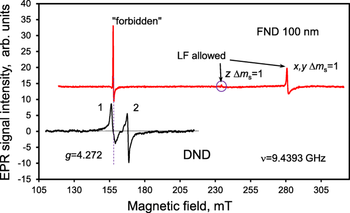
半磁场区域中酸纯化的 DND(黑色曲线)和参考电子辐照荧光 Ib HPHT 金刚石纳米颗粒的 EPR 光谱,平均尺寸为 ~100 nm(红色曲线),范围高达 320 mT。 DND EPR 谱的两条谱线都用数字 1 和 2 标记。带有 g 的低场线 1 =4.272 对应于 NV − 中心。允许与低场 (LF) 相关的线 z Δm s =1 和 x ,y Δm s = 1 transitions in FND 100 nm are marked by arrows for the upper spectrum. The weakest, barely distinguishable line related with allowed z Δm s = 1 transition is additionally marked by a circle. The microwave frequency was 9.4393 GHz

Energy diagram of ground singlet-triplet levels 3 A2 of NV − in magnetic field up to 300 mT. “Forbidden” Δm s = 2 and LF allowed Δm s = 1 transitions caused by absorption of microwave radiation (ν ≈ 9.44 GHz) are marked by vertical red arrows. The position of the ground state spin level anti-crossing (|0 〉GS and |−1〉GS) is marked by a circle

一 Background subtraction in EPR signal of DND and b estimations of the double-integrated intensities of the g = 4.27 line for a DND sample and reference fluorescent Ib HPHT synthetic diamond.面板a :as-registered first derivative EPR signal of the DND in the ± 15 mT half magnetic field range (curve 1, blue); the same, but integrated EPR signal in the same ± 15 mT range of magnetic field (curve 2); the same first derivative EPR signal of DND, but after subtraction of the broad parasitic EPR signal from remaining non-removable iron-containing paramagnetic complexes shown by red contour of Lorentzian shape in the upper curve (curve 3, blue).面板 b :Estimation of the double integrated intensity of the g = 4.27 line for a fluorescent Ib HPHT diamond having NV − (upper curve, shaded area) and the DND sample (bottom curve, shadow area). The bottom spectrum in panel b consists of two contours of Lorentzian shape, one of which centred at lower magnetic field (≈ 150.932 mT), is assigned to the NV − centres of DND (the area below this contour in red is highlighted). Microwave frequency:ν = 9.0785 GHz
The main high-intensity EPR signal of the DND lies above 320 mT at ν = 9.4393 GHz and has a g -factor g ≈ 2.0027. It has a Lorentzian curve profile of linewidth ΔH pp = 0.84 mT [13]. This linewidth is greater than that of fluorescent nanodiamonds (FNDs, 100 nm) milled from microcrystalline diamond synthesized by a high-pressure and high-temperature method. The broad signal can be explained by greater exchange and dipole-dipole interactions between the S = 1/2 spins in the spin ensemble within an individual DND nanoparticle than those within a FND. The intensity of the main EPR signal collected from all S = 1/2 paramagnetic centres, both of nitrogen (P1 centres [28]) and non-nitrogen origin, indicates a spin concentration of ~ 1300 ppm, corresponding Footnote 4 to around 15 S = 1/2 spins in each DND [13]. However, it can be concluded from the earlier obtained data that approximately 40–50% of the total number of all paramagnetic centres in the DNDs are due to half-populated antibonding orbitals of isolated P1 centres. Thus, the huge total of spin-half, point-like agents located in DNDs (N PC) can be represented as the sum of at least two contributions, from P1 centres and from elemental point defects having dangling bond spins ½, for example based on vacancies like H1 centres (VH o ):\( \left({N}_{\mathrm{PC}}=\left[{\mathrm{N}}_{\mathrm{s}}^{\mathrm{o}}\right]+\left[\mathrm{et}\ \mathrm{al}\ \right]\ \right) \). Here we assume that specific EPR signatures from the hyperfine structures of P1 and H1 centres are absent or greatly “smeared” through the dense arrangement of localized spins within each particle. This sum gives us a clue about the approximate content of both isolated nitrogen and monovacancies inside the DND, although isolated nitrogen and monovacancies can also be present in the diamond lattice in nonparamagnetic forms such as \( {\mathrm{N}}_{\mathrm{s}}^{-},{\mathrm{N}}_{\mathrm{s}}^{+} \), V o . The presence of H1 centres together with neutral monovacancies in DND at some minor level (< 700 ppm) is reasonable in principle because rapid assembling of diamond lattice during the detonation takes place from hydrogen-containing products of TNT-hexogen pyrolysis such as CH3 * or CH2 * radicals. Although the mutual charge transfers between the main groups of centres present in the lattice in various charge and spin states (\( {\mathrm{N}}_{\mathrm{s}}^{\mathrm{o}},{\mathrm{N}}_{\mathrm{s}}^{-},{\mathrm{N}}_{\mathrm{s}}^{+};{\mathrm{V}}^{-},{\mathrm{V}}^{\mathrm{o}} \)) are possible in principle, the foremost contribution to paramagnetism comes from only \( {\mathrm{N}}_{\mathrm{s}}^{\mathrm{o}} \). Let us therefore estimate the maximal possible concentration of NV in a DND on the basis of assumptions about the known total amounts of substitutional nitrogen and monovacancies inside the particles. The actual charge state of NV is not essential for such an estimation. A statistical approach gives the following simple formula for the probability (p NV) of finding at least one NV in one 5-nm DND particle consisting of N nodes of covalent diamond lattice:\( {p}_{\mathrm{NV}}=\frac{2 nv}{N} \) , where n and v are the mean numbers of isolated nitrogen atoms and monovacancies inside the DND particle, respectively. Because N PC ≈ 1300 ppm, we can approximately assume that n + v ~ 15 for N = 11,500. The maximal value of p NV is achieved when \( n\approx v\approx \frac{15}{2} \). This gives p NV ≈ 0.0098. This value corresponds to around ~ 1 ppm of NV in DND, as was obtained previously from comparison of the g = 4.27 EPR signals of the DND and the reference sample. Excluding the surface nodes linked with surface functional groups and interior nodes occupied by A-centres (up to 2 at.%) from the formal integration procedure, using N = 9950–10,000 gives a slightly greater concentration of NV, up to 1.1 ppm. The estimated experimental concentration of NV − centres in the DNDs is in close agreement with the theoretical estimation made above, and about 1000 times smaller than the concentration of all S = 1/2 paramagnetic species in the system.
The concentration ratio for interior S = 1/2\( {\mathrm{N}}_{\mathrm{s}}^{\mathrm{o}} \) and S = 1 NV − centres is therefore qualitatively consistent with the main idea of rapid NV centre formation, that is, from the “random inclusion” of both substitutional nitrogen atoms and vacancies to the growing diamond nano-crystallites during the overall ~ 13–20 μs duration of the detonation wave propagation. Here, we intuitively assume that each NV − is formed as a result of the random embedding and occurrence of impurity nitrogen atoms and vacancies in the nearest neighbour lattice sites during the period of time prior to the subsequent rapid cooling of the products to temperatures of the order of ~ 500–650 °C at which the diffusion of vacancies in the lattice is practically stopped.
Nitrogen Impurity Concentrations
XPS is a powerful tool for studying the DNDs’ composition and the chemical state of the main alien elements present on the surface of the DNDs (and also within 2 nm under the surface) [29]. Our main interest was focused on the XPS signal from nitrogen and the evaluation of the interior nitrogen content, since nitrogen is the predominant inner impurity. The XPS signals of carbon (C1s), nitrogen (N1s) and other elements have been recorded after etching of the surface with Ar ions. An overview of the XPS spectrum plotted in the wide range of binding energies from 250 to 600 eV is shown in Fig. 5a. Although the data indicates the presence of a large amount of oxygen-containing atomic groups at the DND’s surface (5.5 at.%), the analysis of the O1s signal is not of particular relevance to this work. The concentration of both inner and exterior nitrogen was preliminarily evaluated to be between 1.7 and 2.4 at.% [30]. The concentration of all the residual elements found (a small number of metals) did not exceed ~ 0.32 at.% in the as-received DND, and it could be reduced by 20–30 times by etching the DND powder in boiling aqua regia and hydrochloric acid [30]. The photoemission peak of nitrogen (N1s) is shown in Fig. 5b. Etching with Ar ions results in the removal of weakly bound adsorbed species from the surface, while the covalent diamond lattice remains unaffected. The characteristic high-energy peaks (~ 404.6 eV and 407.3 eV) in the N1s photoemission signal have very low intensities when compared with an untreated pristine sample. These peaks demonstrate the presence of any remaining nitrate ions (peak at ~ 407.3 eV) and nitrite groups (peak at ~ 404.6 eV) on the Ar ion-treated surface. Further complete removal of nitrate ions and nitrite groups from the surface can be achieved only by annealing the DND powder in air at temperature> 350 o C. The main peak of the N1s signal at ~ 401 eV, which is not influenced by Ar ion treatment, corresponds to chemical bonds of the type N–sp 3 –C. This peak is a characteristic of interior elemental nitrogen covalently bound within the diamond lattice. It appears due to various forms of nitrogen present in the diamond matrix, including NN dimers, next nearest neighbouring N + ...N − pairs, and more complex nitrogen clusters. Similar data were obtained for the photoemission peak of carbon C1s (sharp, intense signal seen in Fig. 5a, see also Ref. [30] for details). The C1s XPS signal consists of two main peaks:one centred at 284.9 eV corresponding to C–C bonds in the diamond matrix and another peak centred at 287.3 eV corresponding to C–N bonds. Only diamond carbon and sp 3 /sp 2 carbon bound to nitrogen, even in the form of atomic-scale disordered nitride phase species (where neighbouring carbon and nitrogen atoms can have up to three C–N bonds), are represented in the C1s signal of the Ar ion-treated surface. Our careful analysis of the integrated intensity of only the N1s 400.9 eV peak and C1s signals (together with O1s and residual elements’ signals) suggests that nitrogen is contained within the diamond lattice of selected DND sample in the amount of 1.65 ± 0.05 at.% and mainly in the form of complex clusters which are not paramagnetic. This value was obtained after special correction by a reducing factor taking into account that the actual size of DND particles is larger than the whole depth of crystal lattice from which the excited photoelectrons are readily emitted. It seems that only a small part of nitrogen is present in the diamond lattice in the form of isolated paramagnetic nitrogen atoms with spin S = 1/2 (no more than 8–9% of all nitrogen). The isolated paramagnetic nitrogen atoms are only accessible for observation by EPR as was shown in the previous section.

XPS spectra of acid-purified DNDs after Ar ion etching:a overview of the spectrum in the range 250-600 eV and b N1s photoemission peaks
XPS spectroscopy was also applied to estimate the nitrogen content in other DND samples provided by our suppliers. We found that the nitrogen content varies in these samples from ~ 1.6 at.% (minimal value) to ~ 2.1 at.% (maximal value). We simultaneously noticed that higher concentrations of nitrogen correspond to the samples with a smaller X-ray CSR size. Such values of nitrogen content were also roughly confirmed by elemental analysis with a Micro Corder JMC10 device in the course of sample combustion in oxygen flow (30 ml/min) at 1000 o C. As a reference source of nitrogen, carbon and hydrogen for this method, we used the antipyrine C11H12N2O, having nitrogen in its structure in the form of N–N groups.
DND Fluorescence Intensity and Its Dependence upon the Nitrogen Content
The PL spectrum of one selected powder DND sample is shown in Fig. 6a. It has the maximum intensity at 680 nm. Following [31], a characteristic spectrum with peak position above 650 nm indicates the presence of both NV − and NV 0 defects, although the contribution from some light-emitting defective sites of remaining sp 2 -coordinated carbon species around DND particles cannot be excluded completely. However, the characteristic zero-phonon lines (ZPL) at 638 nm (NV − ) and 575 nm (NV 0 ), respectively, are not detected. This probably occurs due to the changing positions of the NV 0 and NV − excited/ground states inside the bandgap for centres lying in the vicinity of the particle edge and the subsequent broadening of the 638-nm and 575-nm ZPL spectral components for the ensembles of such NV 0 and NV − centres with slightly different electronic parameters. Let us mark that the absence of featured NV − ZPL peak at 638 nm was confirmed in many studies related with photoluminescence of DND aggregates lying free on the substrate or embedded inside polymers [31]. Sometimes it (suppressed or very poorly recognized ZPL feature at 638 nm) even happens for larger isolated fluorescent Ib HPHT nanodiamonds of a size about 40 nm [4].

一 Photoluminescence spectrum of DND powder pressed flush in a shallow hole with a diameter of 2 mm made in a copper plate and b the interior nitrogen content measured by XPS and c the intensity of NV − PL at 680 nm as a function of X-ray CSR size for a series of selected DNDs synthesized in the presence of some intentionally added inorganic additives in the detonation zone (charge and water shell) as provided by the manufacturer. Excitation laser wavelength λ = 532 nm, power ~ 0.5 mW. The diameter of the focused laser spot on the sample surface was 2 μm. Conditions of recording were temperature T = 293 K, and an air environment
We also studied the PL intensity for a series of DND samples with different CSR sizes. The CSR size characterizes the average size of perfect diamond domains or the mean size of diamond nano-crystallites in the powder even if they are randomly arranged in large-scale polycrystalline aggregates with size exceeding 30–50 nm. The CSR size varied from 4.3 to 5.6 nm in the series of DND samples selected for our studies (similar to the results explained in Ref. [32] although we used another more traditional approach for analysing X-ray diffractograms). Figure 6b shows the dependence of interior nitrogen content evaluated by means of the XPS method versus the CSR size of the DNDs. The larger the CSR size, the smaller the nitrogen content. This seems reasonable as powders with larger DND particles were synthesized as a result of the addition of some inorganic substances having the elements playing the role of nitrogen-getter inside the detonation zone (charge or charge enclosure). Such elementary additives probably promote the reduction of the overall nitrogen content in the growing diamond lattice during the explosion process or change the conditions of the diamond lattice assembly to slightly prolong the synthesis (on the order of microseconds). In addition to the overall nitrogen content, we also recorded the reduced amount of nitrogen-related paramagnetic centres in these DNDs, as confirmed by EPR spectroscopy. PL spectra of all DNDs having different CSR sizes are practically the same in shape in the range 550–900 nm, but this is not the case for the absolute intensities of the PL at the maxima of the PL spectra at 650–680 nm. The intensity at the maximum of PL spectrum is plotted in Fig. 6c as a function of the X-ray CSR size of the DNDs. Comparing both panels (Fig. 6b, c) it is clearly seen that the smaller the nitrogen content in DND, the higher the NV − PL intensity. Again, this seems reasonable as nitrogen-related centres and especially A-centres can act as effective quenchers of PL if the NV − light-emitting centres in some DND particles (one per a hundred of 5 nm DND particles at least) are surrounded by a “gas” of A-centres and other lattice imperfections, similar to the approach proposed in Ref. [33]. This trend gives us a hint at possible ways to enhance the intensity of luminescence from ensembles of DND particles by manipulating their size and nitrogen concentration. Among them, there is the technological enlargement of the mean size of DND particles in the course of their treatment at high pressure and high temperature at appropriate conditions, promoting their recrystallization and further crystal growth [34]. The probable reduction of NV − content through treatment leading to the reduction of A-centres and other interior defects in the diamond lattice may be compensated in principle by the opposite trend, promoting the brightness of NV − emission, and reducing the amount of all types of PL quenchers in the system, and hence, substantially improving the crystal quality of particles with sizes exceeding a dozen nanometres [34, 35]. Further works on these topics are now in progress.
DND Aggregate-Specific Fluorescence and Discrimination of Diffraction-Limited Emitters
Characterizing the fluorescence from isolated DND particles or submicron aggregates is crucial both for understanding their potential use as fluorescent markers and to help to mitigate disadvantages related with a relatively low concentration of NV − in them as determined by EPR. Photoluminescence was recorded for DND aggregates spin-coated on a glass microscope coverslip from an aqueous suspension with an average size of DND aggregates about 30 nm (as measured by dynamic light scattering).
Figure 7a shows two PL 2D maps obtained by confocal microscopy, using a 532-nm wavelength excitation laser with 100-μW output optical power. Bright spots corresponding to DND aggregates up to 500–700 nm in lateral size are observed. Dimmer spots of size around the optical diffraction limit are also observed after selection of the appropriate isolated spots. Figure 7c shows the intensity distribution along the specially selected straight line aa plotted in Fig. 7a. This line crosses about six dim spots of smallest diameter—five spots (1–5) are crossed by the straight line fairly precisely along their centres and one spot (6) is with a small displacement from this line. The corresponding five peaks in intensity distribution are clearly seen in Fig. 7c. Thus, each dim spot 1–5 laying on the line aa corresponds to the DND aggregate of smallest lateral size (in the range below 70 nm). It is possible that all of them are fixed on one V-shaped straight groove existing on the glass coverslip. We successfully fitted each peak in the intensity distribution with a 2D Gaussian \( {A}_i{e}^{-\left[{\left(x-{x}_{oi}\right)}^2+{\left(y-{y}_{oi}\right)}^2\right]/2{s}_i^2} \), where x oi , y oi are the Cartesian coordinates of the centres of the dim round spots, A 我 -maximum PL intensity of each isolated spot, s 我 is a parameter close to s o ≈ r o/3, where s o is a 1/3 part of the Airy disk diameter r 哦。 In our case, for λ = 532 nm radiation (in vacuum) and numerical aperture of microscopic objective NA = 1.40, we have the following values for r o and s o:r o=1.22λ/2NA ≈ 232 nm and s o ≈ 77 nm. The s o value in the 2D Gaussian determines the point spread function (PSF) of and ideal point-like emitter, i.e. the diffraction limitation related with the smallest possible interference ring. For the five peaks mentioned above (i = 1–5) we found the following s 我 values, respectively:85, 77, 77, 84 and 77 nm. Peak 5 has both the highest intensity and s -value equal to the theoretical value s o ≈ 77 nm. This means that the lateral size of the corresponding emitter for peak 5 is significantly smaller than the PSF size. The same is also true for peaks 1–4. We can conclude that the lateral sizes of DND aggregates laying along line aa are in the range below 70 nm. Each spherically shaped DND aggregate of ~ 30 nm in size Footnote 5 consisting of individual 5-nm particles (percentage of voids is 50%) has about 1.3 NV − centres in accordance with the 1.1 ppm content of NV − determined previously. This value is great enough in principle to distinguish aggregates of this size by optical methods. Each of the five aggregates lying along the line aa probably has between 2 and 10 colour centres. The larger the height of the DND aggregate lying on the substrate, the higher the density of luminescence centres (per unit square) for the light emitted more or less perpendicular to the surface. For aggregates with height up to 300–350 nm, the brightness of PL intensity can be at least one order of magnitude greater than that for aggregates of smaller 25–30 nm size. The PL spectrum of one selected aggregate of high brightness (marked by a circle in the 2D map presented in Fig. 7a) was studied in detail. It has roughly the same shape (especially on the right wing above 680 nm) as that for the spectrum shown in Fig. 6a and indicates the presence of both NV − and NV 0 defects. However, the characteristic zero-phonon lines (ZPL) at 638 nm (NV − ) and 575 nm (NV 0 ), respectively, were again not detected. ZPLs are usually well resolved only for diamond crystals of micron size or larger, while for nanometre-scale crystals, they are typically not well-observed due to some experimental or other physical reasons Footnote 6 . Let us mark that for DND aggregates lying on the cover glass, the final treatment with UV/O-Cleaner removed the sp 2 -coordinated carbon species around the particles inside the aggregates and as a result the PL spectrum is free from the contribution of light-emitting centres of disorganized sp 2 -carbon phase.

一 2D-colour mapping of the PL signal intensity of DND spin-coated on a glass microscope coverslip together with b schematics of the experimental setup. c The PL intensity profile along the “aa” cross-section. d The photoluminescence intensity versus time for the selected DND aggregate marked with a circle in the upper side of the 2D map shown in panel a , in the presence or absence of an external magnetic field. Laser excitation at 532 nm wavelength. Square, 201 × 201 pixels. Integration time is 3 ms/pixel. Step—100 nm. The excitation radiation is focused on the upper surface of the glass coverslip with deposited DND. In zero field (B = 0), only small changes of intensity, due to the blinking of some of the NV − colour centres occur. When magnetic field is temporally applied a large decrease of the PL intensity occurs. Upper left panel a :the left scale for PL intensity corresponds to the 2D mapping of another DND aggregate shown in the left bottom corner of the large 2D map. Upper right panel b :schematics of the experimental setup explaining the displacement of the permanent magnet above the coverslip relative to the deposited DND
To confirm the presence of NV − centres in the DND, we studied the influence of an external magnetic field on the PL intensity. No PL modification is expected from NV 0 , which have no magneto-optical properties unlike NV − . Figure 7d shows the meander-like time variation of the PL intensity from an isolated DND aggregate in the presence of an external magnetic field switched “ON” by quickly bringing a compact permanent magnet close to the DND or by removing it (“OFF”). This occurs as a result of the mixing of the |0〉GS and |−1〉GS states of NV − centres at the ground-state spin level anti-crossing (GSLAC), marked with a circle at magnetic field ~ 100 mT in Fig. 3. Such mixing leads to a change in the populations of these states, accompanied by a PL intensity decrease. The optical transitions between the ground 3 A2 and excited 2 E triplet states preserve the spin quantum number (Δm S = 0). However, from the m S = ± 1 excited state, the optical excitation of NV – also decays with no radiation in the visible domain, through a system of two metastable singlet states before coming back to the ground state [5]. This process is accompanied by radiation at a longer wavelength of 1042 nm defined by the gap between these two singlet levels with S = 0. This additional decay pathway results in a lower fluorescence intensity from the main radiation transition within the m S = ± 1 subsystem of ground and excited triplet states. The experimentally detected decrease of NV – centre PL intensity is quite reasonable in the presence of a weak (≤ 100 mT) magnetic field [36], as observed in Fig. 7d. Surprisingly, in our case (for DNDs), this drop is essentially larger than those reported in the literature for Ib HPHT fluorescent microdiamonds and even evaluated theoretically in the framework of the standard NV model [37].
Conclusion
In this article, we have shown that nitrogen-vacancy centres appeared in the interior of 5 nm nanodiamond particles synthesized by detonation of nitrogen-containing explosives are the main triplet colour centres. Precise counting of the number of NV − centres was achieved. The DNDs contain ~ 1.1 ppm of such NV − centres in the crystalline diamond lattice. This value is just five times smaller than that detected in the bright fluorescent reference Ib HPHT diamonds with a mean size of about ~ 100 nm. Our adjusted and rechecked estimation made on the basis of the EPR method is about three orders of magnitude larger than that evaluated in Ref. [38] by pure optical methods for DND aggregates. Probably not all NV − centres detected by EPR are optically active due to the NV − luminescence quenching by various point and collective defects located near the surface. Annealing DNDs in oxygen- or ozone-containing air removes defects associated with light-absorbing sp 2 carbon at the particle surface and allows detection of the specific PL of NV − centres. When an external magnetic field is applied, an accompanying variation of the PL intensity is observed. This is the result of the sensitivity of the NV − triplet ground state to magnetic field and comes through the mixing of the |0〉GS and |−1〉GS states of only the NV − centres below/near the GSLAC point leading to the decay of the optical excitation with no radiation in the visible domain. The application of this effect to discriminate ultra-small DND emitters in an environment with a large autofluorescence background and micron-scale bio-object contouring is promising [39]. Some DND aggregates playing the role of point-like NV − emitters and giving the smallest fluorescent spots with diameter close to the PSF size (diffraction limitation) were found.
Notes
- 1.
The same data for concentration of paramagnetic centres S = ½ (≥ 1260 ppm) were obtained independently by precision measurements of the magnetization field dependence at temperature T = 2 K using a superconducting SQUID magnetometer. The magnetization curve does not show the presence of spins 3/2 in appreciable quantity in DNDs [13].
- 2.
See for example the details of this method for analysis of the standard (DND) and non-standard (NDB-G) samples given in Ref. [22].
- 3.
Fluorescent Ib HPHT (high pressure high temperature) microcrystals doped with nitrogen (100–150 ppm) and thereafter irradiated by high energy electrons (2–15 MeV) and annealed at 800–950 o C.
- 4.
We assume that a typical DND particle (with size slightly exceeding 5 nm) consists of ~ 1.1 × 10 4 carbon atoms.
- 5.
Here we consider the typical DND aggregate in water DND suspension used for deposition the aggregates on the glass coverslip. Certainly, the actual shape of aggregates lying on the cover slip can be rougher and extremely diverse depending upon the adhesion of DND particles to the glass and actual size of the large-scale aggregates.
- 6.
The ZPL line at 638 nm was not resolved in many works where the nanodiamonds having NV − were studied [4, 31]. It is probable that the various local environments of NV − centres in nanosized diamond (like surface defects and interior imperfections) greatly disturb the position of NV − triplet ground states in the bandgap.
缩写
- 2D:
-
Two dimensional
- CCD:
-
Charge-coupled device
- DND:
-
Detonation nanodiamond
- EPR:
-
Electron paramagnetic resonance
- FND:
-
Fluorescent nanodiamond
- GSLAC:
-
Ground state spin levels anti-crossing
- HPHT:
-
High pressure high temperature
- NA:
-
Numerical aperture
- NV:
-
Nitrogen-vacancy
- ODMR:
-
Optically detectable magnetic resonance
- PL:
-
光致发光
- PSF:
-
Point spread function
- SCTB:
-
Special design and technology bureau
- SQUID:
-
Superconducting quantum interference device
- UV:
-
Ultraviolet
- XPS:
-
X射线光电子能谱
- XRD:
-
X射线衍射
- ZPL:
-
Zero-phonon line
纳米材料