

通过局部调制 n-AlGaN 层中的掺杂类型来改善基于 AlGaN 的深紫外发光二极管的电流扩展
摘要
在本报告中,我们局部调节了 n 中的掺杂类型 -AlGaN 层通过为基于 AlGaN 的深紫外发光二极管 (DUV LED) 提出 n-AlGaN/p-AlGaN/n-AlGaN (NPN-AlGaN) 结构的电流扩展层。在 n-AlGaN 电子供应层中插入薄的 p-AlGaN 层后,可以在 n 中产生导带势垒 型电子供应层,它能够调制 DUV LED 的 p 型空穴供应层中的横向电流分布。此外,根据我们的研究,发现 Mg 掺杂浓度、厚度、p-AlGaN 插入层的 AlN 成分和 NPN-AlGaN 结数对电流扩展效果有很大影响。适当设计的NPN-AlGaN电流扩展层可以提高DUV LED的光输出功率、外量子效率(EQE)和壁插效率(WPE)。
介绍
由于消毒、水净化、医疗和高密度光学记录等各种应用[1,2,3,4,5,6,7,8],人们投入大量精力开发高效的AlGaN-基于深紫外发光二极管(DUV LED)。现阶段,在提高富铝 AlGaN 薄膜的结晶质量方面取得了显着进展,例如,通过石墨烯辅助准范德华外延在纳米图案蓝宝石衬底上生长 AlN 薄膜可以大大释放应变并降低位错密度 [9],表明内部量子效率 (IQE) 为 80% [10]。值得注意的是,这种IQE是使用低温光致发光方法测量的,该方法不涉及任何载流子注入。然而,DUV LED 是通过电偏压操作的,这与电流和载流子传输有关 [11,12,13]。关于电流流动的另一个非常重要的方面是电流拥挤效应,当器件偏置在非常高的电流水平时很容易发生 [14]。 DUV LED 在具有高 AlN 成分的 p-AlGaN 层中具有非常差的 Mg 掺杂效率 [15, 16],导致低导电率。此外,DUV LED采用倒装芯片结构,具有电流横向注入方案。因此,与基于 InGaN/GaN 的 UV、蓝色和绿色 LED 相比,基于 AlGaN 的 DUV LED 受到当前拥挤效应的挑战更大 [17]。在 p 接触电极或台面边缘发生电流拥挤效应会导致多量子阱 (MQW) 中的电致发光强度不均匀和结温升高 [18]。因此,促进 DUV LED 的横向电流扩展确实至关重要。为此,所提出的窄多条 p 型电极能够实现均匀分布的电流分布,从而将壁插效率 (WPE) 提高 60% [19]。此外,ITO/ZGO (ZnGaO) 电流扩展层可以更好地扩展电流并提高外部量子效率 (EQE),但 ZGO/p-GaN 界面处增加的界面电阻率使得 DUV LED 的 WPE 增强较少 [20] .
因此,现阶段的研究重点放在 p 侧,以促进 DUV LED 的电流扩散。在这项工作中,与其他方法不同,我们提出并证明可以通过设计 n-AlGaN 电子供应层来实现 DUV LED 的 p 型空穴供应层中改进的电流分布。通过调制电子供应层中的掺杂类型,在导带中产生能垒,即提出并参数化研究了 n-AlGaN/p-AlGaN/n-AlGaN (NPN-AlGaN) 结构。我们的结果表明,通过使用 NPN-AlGaN 结可以使空穴的横向分布均匀化,从而提高了 DUV LED 的光输出功率、外部量子效率和壁插效率。我们设计的另一个优点是,从外延生长的角度来看,在 n 型电子供应层中设置电流扩展层可以让外延生长者在优化生长条件方面有更多的自由。
研究方法和物理模型
NPN-AlGaN DUV LED 结构示意图如图 1a 所示。在每个研究的 DUV LED 中,我们有一个 4 微米厚的 n-Al0.60Ga0.40N/p-Alx Ga1−x N/n-Al0.60Ga0.40N层,n-Al0.60Ga0.40N区的Si掺杂浓度为5×10 18 厘米 −3 .然后,设计了五对Al0.45Ga0.55N/Al0.56Ga0.44N多量子阱(MQW)有源层,其量子阱和量子势垒的厚度分别为3 nm和12 nm。 MQW 被 18 纳米厚的 Mg 掺杂 p-Al0.60Ga0.40N 层作为 p-EBL 覆盖,然后是 50 纳米厚的 Mg 掺杂 p-Al0.40Ga0.60N 层和一个接着是 50 纳米厚的掺镁 p-GaN 层。 p-EBL 和空穴供应层的空穴浓度设置为 3 × 10 17 厘米 −3 .我们设计了具有 350 × 350 μm 2 的矩形台面的器件几何结构 .图 1b 显示了 DUV LED 结构中采用两个 NPN-AlGaN 结(即 NPNPN-AlGaN 结构)时的导带剖面示意图,我们可以看到耗尽的 p-Alx 中存在能垒。我> Ga1−x N 个区域。能垒可以调整p型空穴供应层中的水平电流分布。注意,为了保证电流通过反向偏置的 n-AlGaN/p-AlGaN 结,使 p-AGaN 插入层完全耗尽非常重要,这样 NPN-AlGaN 结将处于穿透击穿模式[21]。随后将进行详细的分析和讨论。我们的参考 DUV LED 与 NPN-AlGaN DUV LED 相同,只是使用 4 μm 厚的 Si 掺杂 n-Al0.60Ga0.40N 层作为电子供应层。
<图片>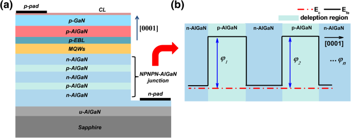
一 NPN-AlGaN LED 的结构示意图。 b 具有两个 NPN-AlGaN 结的 NPNPN-AlGaN 结构的导带剖面示意图;我们将每个 NPN-AlGaN 结的势垒高度定义为 φ 1、φ 2、φ n , 和 n 是 NPN-AlGaN 结的数量
为了更好地理解 NPN-AlGaN 结实现的改进电流扩展效应的物理机制,图 2a 显示了具有横向电流注入方案的 DUV LED 的等效电路。我们可以看到电流从 p 型空穴供应层沿垂直和横向两个方向流向 n-AlGaN 区域。如果 n-AlGaN 电子供应层的电阻小于电流扩展层 (CL) 的电阻,则电流趋向于聚集在 p 型欧姆接触下方的区域,即 I 1> 我 2> 我 3> ...> 我 n [14]。在 DUV LED 结构中加入 NPN-AlGaN 结可以抑制破坏性的电流拥挤效应。然后,我们进一步简化了图 2b 中 NPN-AlGaN DUV LED 的电流路径,使得总电流可以分为垂直部分(I 1) 和水平部分 (I 2) 从点A 指向 B .因此,两点之间的总电压由电流扩展层、p-GaN 层、p-AlGaN 层、MQW、NPN-AlGaN 结和 n-AlGaN 层共享。基于I的当前路径 1 和 I 2,方程。分别得到 1 和 2,并通过求解前两个公式,方程。然后推导出3:
$$ {I}_1{R}_{\mathrm{CL}-\mathrm{V}}+{I}_1{R}_X+{I}_1\bullet N\bullet {R}_{npn}+{ I}_1\left({R}_{n-\mathrm{V}}+{R}_{nL}\right)={U}_{\mathrm{AB}}, $$ (1) $$ {I}_2\left({R}_{\mathrm{CL}-\mathrm{L}}+{R}_{\mathrm{CL}-\mathrm{V}}\right)+{I}_2 {R}_X+{I}_2\bullet N\bullet {R}_{npn}+{I}_2{R}_{n-\mathrm{V}}={U}_{\mathrm{AB}} , $$ (2) $$ \frac{I_1}{I_2}=1+\frac{R_{\mathrm{CL}-\mathrm{L}}-{R}_{n-\mathrm{L}} {R_{\mathrm{CL}-\mathrm{V}}+{R}_X+{R}_n+N\bullet {R}_{npn}} $$ (3) <图片>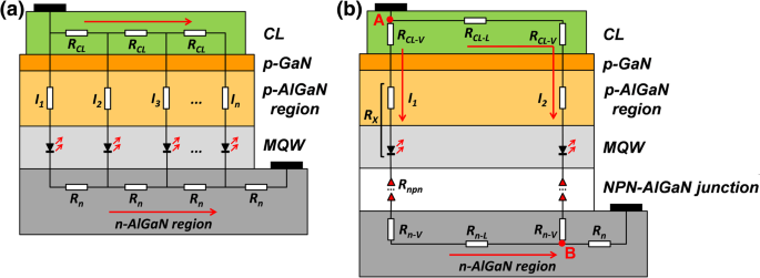
一 具有横向电流注入方案等效电路 (I 1> 我 2> 我 3> ……> 我 n )。 b NPN-AlGaN 结构的 DUV LED 简化等效电路和电流路径 I 1 和 I 2个展出
其中 R CL−V 和 R CL−L 分别是电流传播层的垂直和水平电阻; R n -V 和 R n -L 分别表示 n-AlGaN 层的垂直和水平电阻; R n 是 R 的总和 n -V 和 R n -L (即,R n =R n -V + R n -L ) 对于当前路径 I 1; p型空穴注入区和MQW区的电阻总和由R表示 x; R npn 是由每个 NPN-AlGaN 结中的势垒高度引起的界面电阻; N 表示 NPN-AlGaN 结的总数,以及 A 点之间的总电压降 和 B 由 U 描述 AB .值得一提的是,对于所有研究的器件,200 nm 厚的电流扩展层比 4 μm 厚的 n-AlGaN 电子供应层薄得多。因此,获得了电阻比 n-AlGaN 层大得多的 CL,即 R CL−L - R n -L ≫ 0. 显然 I 的比值 1/我 2 可以通过使 N 减少 × R npn 价值增加。 因此,通过在 DUV LED 结构的 n 型电子供应层中使用 NPN-AlGaN 结,可以改善 p 型空穴供应层中的电流扩展效应。一方面,N × R npn 可以通过增加 N 来提高价值 .另一方面,R 的值 npn 受 AlN 成分、厚度和 p-AlGaN 插入层的 Mg 掺杂浓度影响。因此,将在后续讨论中进行详细分析。
Crosslight APSYS 模拟器用于研究器件物理,根据我们之前关于蓝色、UVA 和 DUV 氮化物 LED [22,23,24] 的出版物,我们使用的模型是可靠的。在我们的物理模型中,AlGaN/AlGaN 异质结的能带偏移比设置为 50:50 [25]。俄歇复合系数、肖克利-雷德-霍尔 (SRH) 复合寿命和光提取效率设置为 1.0 × 10 -30 厘米 6 DUV LED 分别为 /s [26]、10 ns [27] 和 ~ 8% [28]。假设极化水平为40%[29],考虑晶格失配界面的极化诱导界面电荷。
结果和讨论
NPN-AlGaN 结构对 DUV LED 电流扩散效应的影响
LED A(即,没有 NPN-AlGaN 结的参考 DUV LED)和 LED B(即,具有 NPN-AlGaN 结的 DUV LED)已被首先研究,以探讨 NPN-AlGaN 结构对电流均质化的影响。 p 型空穴供应层。每个NPN-AlGaN结都有一个20nm厚的p-Al0.60Ga0.40N插入层,其Mg掺杂浓度为1×10 18 厘米 −3 .图3a为电流密度为170 A/cm 2 时的能带分布 对于 LED B,在 NPN-AlGaN 结中形成导带中的两个能垒,该能垒的形成很好地归因于插入的 p-Al0.60Ga0.40N 层的耗尽效应。 LED B 中产生的势垒会导致 R 的界面电阻 npn 在 NPN-AlGaN 结区,这有助于降低 I 1/我 2 如方程式中所述。 3,这样更多的空穴将沿着当前路径I流动 2. 然后我们计算并显示当电流密度为 170 A/cm 2 时 LED A 和 B 的最后一个量子阱 (LQW) 中的水平空穴浓度 ,如图 3b 所示。我们可以清楚地看到,与 LED A 相比,LED B 获得了更好的横向电流扩展。 因此,我们证明了 n 型电子供应层中的 NPN-AlGaN 促进了 p 型空穴供应层中的电流扩展效应DUV LED。
<图片>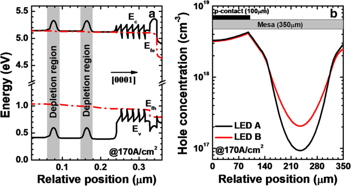
一 LED B 的能带分布,其中我们将导带、电子和空穴的准费米能级以及价带定义为 E c , E 铁 , E fh , 和 E v , 分别。 b 当电流密度为 170 A/cm 2 时,LED A 和 B 的 LQW 中的水平空穴浓度
除了显示横向空穴浓度外,我们还展示了图 4a 中 LED A 和 B 的 MQW 中的空穴浓度水平。我们可以看到,由于电流扩散效应的改善,与 LED A 相比,LED B 的 MQW 中的空穴浓度提高。 MQW 中提高的空穴浓度水平更有利于 LED B 的辐射复合(参见图4b).
<图片>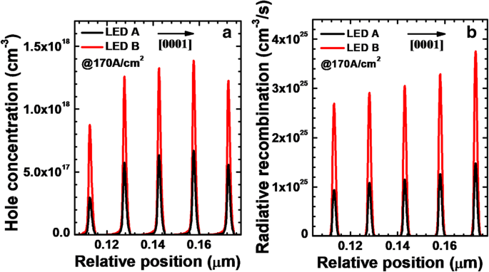
一 空穴浓度水平和b 分别为 LED A 和 B 的 MQW 中的辐射复合分布。当电流密度为170 A/cm时,我们在距台面右边缘120 μm处采集数据 2
NPN-AlGaN 结的影响也可以通过计算出的 LED A 和 B 的光学和电学性能来证明,如图 5 所示。图 5a 显示了作为两个 LED 注入电流的函数的 EQE 和光功率密度A 和 B。我们可以看到 LED B 具有比 LED A 更高的 EQE 和光功率密度,这要归功于 NPN-AlGaN 结实现的改进的电流扩展效果和空穴注入效率。例如,当电流密度为 170 A/cm 2 时,LED B 的光功率密度增强为 ~ 1.67% 根据图5a。图 5b 中的研究表明,与 LED A 相比,具有 NPN-AlGaN 结的 LED B 的正向电压略有增加。我们将这种现象归因于 NPN-AlGaN 引起的耗尽区中的能垒路口。幸运的是,LED B 较高的正向电压不会对墙插效率 (WPE) 产生不利影响,并且当注入电流密度大于 ~ 56 A/cm2 如图5c所示。我们认为,一旦优化 NPN-AlGaN 结,就可以同时实现增强的 EQE 和 WPE,具体研究如下。
<图片>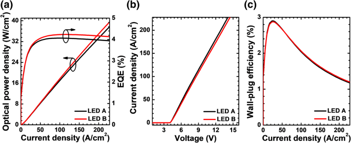
一 注入电流方面的 EQE 和光功率密度,b 电流-电压特性,c WPE 作为 LED A 和 B 注入电流的函数
p-AlGaN 层的 AlN 成分对电流扩散效应的影响
在本节中,研究了 NPN-AlGaN 结的 AlN 成分对 DUV LED 光学和电学特性的影响。为了清楚地说明这种机制,我们使用了五个 DUV LED,即 LED Ci (i =1、2、3、4 和 5) 具有不同的 NPN-Alx Ga1−x N 结,其中 p-Alx 的 AlN 组成 Ga1−x N 插入层分别为 0.60、0.63、0.66、0.69 和 0.72。 p-Alx的掺杂浓度和厚度 Ga1−x N层为1.8×10 18 厘米 −3 和 20 nm,分别。两个 NPN-AlGaN 结,即 NPNPN-AlGaN 结用于所有研究的器件。然后我们计算每个 NPN-Alx 的导带势垒高度 Ga1−x LED 的 N 结 Ci (i =1, 2, 3, 4, 和 5),如表 1 所示。很明显,随着 p-Alx 的 AlN 成分的增加,传导势垒高度的值增加 Ga1−x N 插入层增加。高传导势垒高度可使R的值 npn 增加,而 I 的比例减少 1/我 2 被同时触发,如等式中所述。 3. 为了证明这一点,当电流密度为 170 A/cm 2 时,所有研究器件的最后一个量子阱中的横向空穴分布 计算并显示在图 6a 中。对于LED C1,采用NPN-Al0.60Ga0.40N结构后可以调节空穴分布,很明显,一旦p-AlGaN插入层的AlN成分增加到0.63,电流扩散效果得到进一步改善我们的结构。
<图片>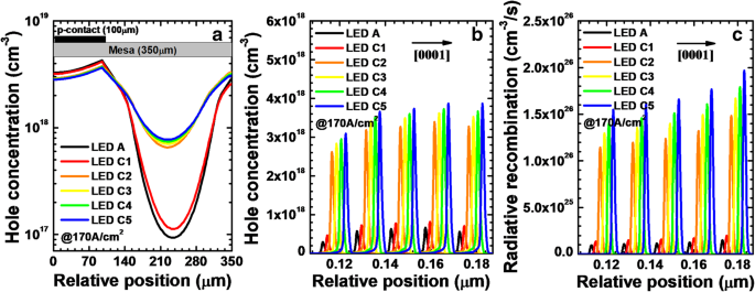
一 LQW 中的水平空穴浓度,b 空穴浓度水平和 c LED A 和 Di 的 MQW 中的辐射复合分布 (i =1, 2, 3, 4, 5) 当电流密度为 170 A/cm 2 .我们故意移动 b 的曲线 和 c 2 nm 更容易识别
我们展示了 LED A 和 Ci MQW 中模拟的空穴浓度水平和辐射复合分布 (i =1, 2, 3, 4, 5) 图 6b 和 c 当电流密度为 170 A/cm 2 , 分别。空穴浓度水平和辐射复合分布在距台面右边缘 120 μm 的位置收集。我们将图 6b 和 c 中研究的 DUV LED 的空穴浓度水平和辐射复合分布分别在空间上移动了 2 nm,以便于识别。对于 LED A,可以清楚地观察到 MQW 中最低的空穴浓度,因此,最低的辐射复合也显示在图 6c 中。由于采用NPN-AlGaN结,MQW中的空穴浓度和辐射复合增加,并且随着p-AlGaN插入层中AlN成分的增加,它们可以进一步增加。
图 7a 中研究的 LED 的光功率密度和 EQE 作为注入电流密度的函数被进一步计算和展示。如图所示,采用NPN-AlGaN结后,EQE和光功率密度增加。此外,随着 p-AlGaN 插入层的 AlN 成分的增加,可以进一步提高 EQE 和光功率密度。我们对此做出了贡献,如图 6a 所示,MQW 中的横向孔分布更加均匀。 LED A 和 Ci 的电流-电压特性 (i =1、2、3、4 和 5)如图 7b 所示。与 LED A 相比,LED C1 的正向电压略有增加,而 LED C5 的正向电压最大。插图显示了当电流密度为 170 A/cm 2 时所有研究 LED 的正向电压 .值得注意的是,与 LED A 相比,LED C2、C3 和 C4 的正向电压降低。 虽然 NPN-AlGaN 结增加了 DUV LED 的垂直电阻,但沿水平方向更均匀的载流子浓度提高了水平电导率,从而导致正向电压降低。这表明只要电流扩散层设计得当,增强的电流扩散效应有助于降低 DUV LED 的正向工作电压 [30]。然而,我们的设计通过引入势垒来调节电流路径,因此,过高的势垒高度可能会牺牲电导率 [21],例如 LED C5。
<图片>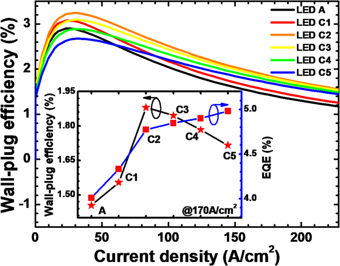
一 注入电流和 b 方面的 EQE 和光功率密度 LED A 和 Ci 的电流-电压特性 (i =1、2、3、4 和 5)。插图:LED A 和 Ci 的正向电压 (i =1, 2, 3, 4, 5) 当电流密度为 170 A/cm 2
图 8 展示了所有研究器件的 WPE 作为注入电流密度的函数。与 LED A 相比,一旦采用 NPN-AlGaN 结,LED C1 的 WPE 就会增加。 LED Ci 的 WPE (i =2, 3, 4, 和 5) 当 NPN-AlGaN 结的 p-AlGaN 层的 AlN 成分增加时,可以进一步改善。然而,尽管 LED Ci 的光功率密度相对较低,但 LED C2 由于最低的正向工作电压而显示出最高的 WPE (i =2、3、4 和 5)。此外,我们还展示了注入电流密度为 170 A/cm 2 时的 WPE 和 EQE 对于插图中的所有研究设备。众所周知,在高注入电流密度下,电流拥挤效应很严重。 LED C5 的 NPN-AlGaN 结在均质电流方面发挥最佳作用。然而,一旦正向工作电压显着增加,WPE 并不令人满意。因此,在获得EQE和WPE的增强之前,必须充分优化NPN-AlGaN结p-AlGaN插入层的AlN成分值。
<图片> LED A 和 Ci 的 WPE 与注入电流的关系 (i =1、2、3、4 和 5)。插图:当电流密度为 170 A/cm 2 时,所研究的 LED 的 EQE 和 WPE,其结构为具有各种 AlN 成分的 p-AlGaN 层
p-AlGaN 层的 Mg 掺杂浓度对电流扩展效应的影响
NPN-AlGaN 结耗尽区的宽度可以通过改变 p-AlGaN 插入层的 Mg 掺杂浓度来控制,导带势垒高度也将相应改变。因此,R 的值 npn 一旦 NPN-AlGaN 结的耗尽区变宽,I 的值可以增加 1/我 2 将减少,即可以改善 DUV LED 的电流扩展效果。为了更好地阐明这一点,我们设计并研究了五个具有不同 Mg 掺杂浓度的 DUV LED,用于 NPN-AlGaN 结中的 p-AlGaN 插入层。我们将 p-AlGaN 层的 Mg 掺杂浓度设置为 3 × 10 17 , 7.5 × 10 17 , 1.7 × 10 18 , 2 × 10 18 , 和 3 × 10 18 厘米 −3 用于 LED Di (i =1、2、3、4 和 5),分别。 p-AlGaN 插入层的厚度和 AlN 成分分别为 20 nm 和 0.61。我们采用两个 NPN-AlGaN 结。如表 2 所示,导带势垒高度随着 p-AlGaN 层 Mg 掺杂浓度的增加而增加。然后,我们计算并展示了当电流密度为 170 A/cm 2 时最后一个量子阱中的横向空穴浓度 在图 9a 中,很明显,与 LED A 的横向孔分布相比,当 DUV LED 引入 NPN-AlGaN 结时,横向孔分布变得更加均匀。此外,随着NPN-AlGaN结中p-AlGaN层的Mg掺杂浓度的增加,可以获得更加均匀的空穴分布。
<图片>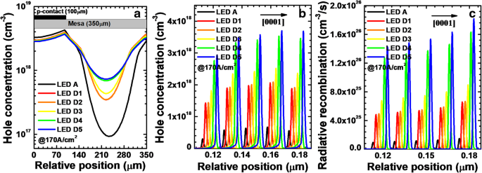
一 LQW 中的水平空穴浓度,b 空穴浓度水平和 c LED A 和 Di 的 MQW 中的辐射复合分布 (i =1, 2, 3, 4, 5) 当电流密度为 170 A/cm 2 .我们故意移动 b 的曲线 和 c 2 nm 更容易识别
然后,当电流密度为 170 A/cm 2 时,图 9b 和 c 中所有研究的 LED 证明了 MQW 中计算的空穴浓度水平和辐射复合分布 ,分别,并且数据收集的位置距离右台面边缘120 μm。正如预期的那样,LED Di (i =1、2、3、4 和 5) 与 LED A 相比,MQW 中的空穴浓度水平和辐射复合分布更高,而空穴浓度和辐射复合随着 p-AlGaN 层中 Mg 掺杂浓度的增加而增加用于具有 NPN-AlGaN 结的 LED。我们为 LED Di 贡献了 MQW 中不断上升的空穴浓度 (i =1, 2, 3, 4, 5) 到增强的电流扩展效应。
由于减少的电流拥挤效应和 MQW 中空穴浓度的上升,LED Di (i =1、2、3、4 和 5)相应地显示了提升的 EQE 和光功率密度(见图 10a)。 LED A 和 Di 的电流-电压特性 (i =1、2、3、4 和 5)如图 10b 所示。显然,LED 的正向工作电压 Di (i =1、2、3、4 和 5) 随着 p-AlGaN 插入层 Mg 掺杂浓度的增加而增加。其中,LED D5显示出最大的开启电压,这归因于p-AlGaN层中Mg掺杂浓度非常高导致的寄生二极管。根据图 10b 的插图,还可以看出,当注入电流密度为 170 A/cm 2 时,LED D5 在所有研究的 LED 中显示出最大的正向工作电压 .
<图片>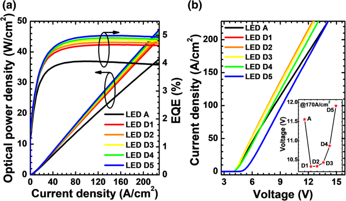
一 注入电流和 b 方面的 EQE 和光功率密度 LED A 和 Di 的电流-电压特性 (i =1、2、3、4 和 5)。插图:LED A 和 Di 的正向电压 (i =1, 2, 3, 4, 5) 当电流密度为 170 A/cm 2
为了进行更全面的分析,我们将 WPE 计算为所有研究 LED 的注入电流密度的函数,如图 11 所示。 LED Di 的 WPE (i =1, 2, 3, 4) 高于 LED A。只有当注入电流密度大于 43 A/cm 2 时,LED D5 的 WPE 才超过 LED A . LED D5 在电流密度小于 43 A/cm 2 时的较低 WPE 是由于前面提到的 NPN-AlGaN 结处的额外正向电压消耗。从插图中可以看出,随着 p-AlGaN 层 Mg 掺杂浓度的增加,EQE 呈上升趋势。然而,随着 p-AlGaN 层的 Mg 掺杂浓度的进一步增加,WPE 降低。因此,我们得出结论,电流扩展效应和正向电压对p-AlGaN插入层的Mg掺杂水平非常敏感。
<图片>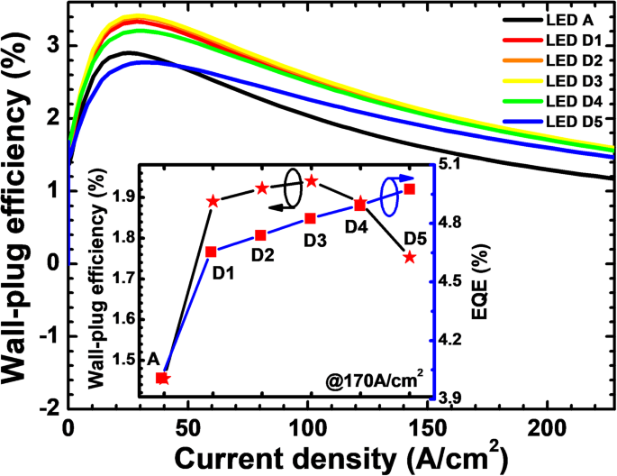
WPE 与 LED A 和 Di 注入电流的关系 (i =1、2、3、4 和 5)。插图:当电流密度为 170 A/cm 2 时,所研究的 LED 的 EQE 和 WPE 结构具有不同掺杂浓度的 p-AlGaN 层
p-AlGaN 层的厚度对电流扩散效应的影响
在本节中,研究了 NPN-AlGaN 结中 p-AlGaN 插入层的厚度对 LED 性能的影响。首先,所有研究的DUV LED均采用两个NPN-AlGaN结(即NPPNN-AlGaN结),其中NPN-AlGaN结中p-AlGaN层的AlN成分和掺杂浓度分别为0.61和1.5 × 10 18 厘米 −3 , 分别。然后,我们为 LED Ti 中的 p-AlGaN 层设置不同的厚度,分别为 18、20、24、28 和 32 nm (i =1、2、3、4 和 5),分别。计算出的每个 NPN-AlGaN 结的导带势垒高度如表 3 所示。可以看出,当 NPN-AlGaN 结中的 p-AlGaN 层变厚时,导带势垒高度增加,这使得 <我>我 1/我 2 和相应的改进的电流扩展。
我们计算并显示 LED A 和 Ti 的 LQW 中的水平空穴浓度 (i =1, 2, 3, 4, 5) 当电流密度为 170 A/cm 2 在图 12a 中。显然,当 NPN-AlGaN 结引入 DUV LED 结构时,空穴分布变得更加均匀,如果 NPN-AlGaN 结中 p-AlGaN 层的厚度变大,则空穴分布会变得更加均匀。减小的电流拥挤效应归因于 NPN-AlGaN 结中增厚的 p-AlGaN 层导致耗尽区中更高的导带势垒高度。 Figure 12b and c exhibit the hole concentration levels and radiative recombination profiles, respectively, for LEDs A and Ti (i =1, 2, 3, 4, and 5) at the injection current density of 170 A/cm 2 . The hole concentration levels and radiative recombination profiles are collected at the location of 120 μm away from the right-hand edge of the mesa. We can see that, when compared to that of LED A in the MQWs, LEDs Ti (i =1, 2, 3, 4, and 5) show the higher hole concentration levels and thus higher radiative recombination profiles. Once the thickness of the p-AlGaN layer is increased, further enhanced hole concentration and radiative recombination in the MQWs can be obtained.

一 Horizontal hole concentration in the LQW, b hole concentration levels, and c radiative recombination profiles in the MQWs for LEDs A and Ti (i =1, 2, 3, 4, and 5) when the current density is 170 A/cm 2 . We purposely shift the curves for b 和 c by 2 nm for easier identification
The observed optical power density and EQE for all studied LEDs in Fig. 13a agree well with the results shown in Fig. 12c, such that the increasing thickness for the p-AlGaN layer in the NPN-AlGaN junction can improve the optical power density and EQE. Moreover, we calculate and show the current-voltage characteristics for LEDs A and Ti (i =1, 2, 3, 4, and 5) in Fig. 13b. It shows that the forward operating voltages for LEDs Ti (i =1, 2, 3, and 4) exhibit a significant reduction when compared to that for LED A at the injection current density larger than 102 A/cm 2 , which is due to the significantly improved current spreading effect after adopting the NPN-Al0.61Ga0.39N junction as mentioned previously. However, a too thick p-AlGaN layer can cause an increase in the turn-on voltage owing to the parasitic N-AlGaN/P-AlGaN diode, e.g., LED T5 has the highest forward operating voltage among all the investigated LEDs when the current density is 170 A/cm 2 , which is also shown in the inset figure of Fig. 13b.

一 EQE and optical power density in terms of the injection current and b current-voltage characteristics for LEDs A and Ti (i =1, 2, 3, 4, and 5). Inset:the forward voltages for LEDs A and Ti (i =1, 2, 3, 4, and 5) when the current density is 170 A/cm 2
To this end, it is particularly important to further discuss the impact of higher forward operating voltage on DUV LED performance. Therefore, we calculate the WPE for all investigate devices and show the results in Fig. 14. We can see that the WPE for all LEDs with NPN-AlGaN junction exhibits distinct enhancement when compared to that for LED A. The presented WPEs in the inset figure also indicate that the NPN-AlGaN-structured DUV LED can save more electrical power than LED A. It is worth mentioning that the thickness for the p-AlGaN layer cannot be improved blindly, such that only when the thickness is properly set, then fully maximized WPE can be obtained.

Relationship between WPE and the injection current for LEDs A and Ti (i =1, 2, 3, 4, and 5). Inset:the EQE and WPE for the investigated LEDs structured with a p-AlGaN layer with various thicknesses when the current density is 170 A/cm 2
Effect of the NPN-AlGaN Junction Number on the Current Spreading Effect
Finally, we investigate the influence of the NPN-AlGaN junction number on the current spreading effect. The p-Al0.61Ga0.39N layer is adopted in the NPN-AlGaN junction for the proposed DUV LEDs in this section, for which the Mg doping concentration and thickness are 1.5 × 10 18 厘米 −3 and 20 nm, respectively. LEDs Ni (i =1, 2, 3, 4, and 5) have 1, 2, 3, 4, and 5 NPN-AlGaN junctions, respectively. As presented in Table 4, the conduction barrier heights of all NPN-AlGaN junctions are almost the same for LEDs Ni (i =1, 2, 3, 4, and 5). However, the total conduction barrier height for NPN-Al0.61Ga0.39N junctions in each investigated DUV LED surely increases when more NPN-Al0.61Ga0.39N junctions are utilized. Thus, the value of N × R npn can be enhanced, which helps to better spread the current horizontally, i.e., the increased value of I 2 in Eq. 3 is favored. The enhanced current spreading effect can be observed in Fig. 15a. The hole concentration in the LQW can become more uniform if the NPN-AlGaN junction number becomes more.

一 Horizontal hole concentration in the LQW, b hole concentration, and c radiative recombination profiles in the MQWs for LEDs A and Ni (i =1, 2, 3, 4, and 5) when the current density is 170 A/cm 2 . We purposely shift the curves for b 和 c by 2 nm for easier identification
Then, the hole concentration levels and radiative recombination profiles in the MQWs for LEDs Ni (i =1, 2, 3, 4, and 5) when the current density is 170 A/cm 2 are exhibited in Fig. 15b and c, respectively. We collect the hole concentration levels and radiative recombination profiles at the location of 120 μm away from the right-hand mesa edge. The hole concentration and radiative recombination are improved by using the NPN-Al0.61Ga0.39N junction, and further improvement can be obtained when more NPN-AlGaN junctions are included. Ascribed to the enhanced hole concentration in the MQWs, the optical power density and EQE for the DUV LEDs with NPN-AlGaN junction also shows a significant improvement. The current-voltage characteristics for all studied devices are shown in Fig. 16b, which illustrates that the forward operating voltages for LEDs Ni (i =1, 2, 3, 4, and 5) are lower than that for LED A, and this indicates that the current spreading effect can help to reduce the forward voltage once the Mg doping concentration, thickness, and AlN composition for the p-AlGaN layer are appropriately applied to the NPN-AlGaN junction. The turn-on voltage for all LEDs with NPN-AlGaN junction is almost the same as that for LED A, which illustrates the negligible impact of the reversely biased N-AlGaN/P-AlGaN parasitic junction if the Mg doping concentration in the p-AlGaN layer is properly set, i.e., the p-AlGaN layer has to be completely depleted before the device is biased.

一 EQE and optical power density in terms of the injection current and b current-voltage characteristics for LEDs A and Ni (i =1, 2, 3, 4, and 5). Inset:the forward voltages for LEDs A and Ni (i =1, 2, 3, 4, and 5) when the current density is 170 A/cm 2
Last but not the least, the WPEs have also been demonstrated for LEDs Ni (i =1, 2, 3, 4, and 5) in Fig. 17. The WPEs of all DUV LEDs with NPN-Al0.61Ga0.39N junction have been promoted owing to the reduced forward operating voltage. In the inset figure, we show the EQE and WPE for LEDs A and Ni (i =1, 2, 3, 4, and 5) when the current density is 170 A/cm 2 . Although the EQE and WPE for LEDs Ni (i =1, 2, 3, 4, and 5) increase with the increasing of the NPN-AlGaN junction number, clearly, we can see that the magnitude of the increase is gradually decreasing, which indicates that the NPN-AlGaN junction number also shall be set to a proper number, and we firmly believe that the device will consume more electrical power if too many NPN-AlGaN junctions are adopted in DUV LEDs.

Relationship between WPE and the injection current for LEDs A and Ni (i =1, 2, 3, 4, and 5). Inset:the EQE and WPE for the investigated LEDs structured with various NPN-AlGaN number when the current density is 170 A/cm 2
结论
To conclude, we have suggested embedding the NPN-AlGaN junction in the n-type electron supplier layer for DUV LEDs. After comprehensive and systematic discussions, we find that the NPN-AlGaN junction can reduce the current crowding effect in the p-type hole supplier layer and improve the hole injection for DUV LEDs. The NPN-AlGaN junction can tune the conductivity for the n-type electron supplier layer so that the current path in the p-type hole supplier layer can be manipulated. For further explorations, we have investigated the impact of different parameters for NPN-AlGaN junctions on the current spreading effect, the EQE, and the WPE. We find that the current can be further homogenized if the AlN composition, the Mg doping concentration, the thickness of the p-AlGaN insertion layer, and the NPN-AlGaN junction number are increased properly. Although the EQE can be promoted by using the proposed NPN-AlGaN junctions, the WPE is not always monotonically improving, which arises from the additional voltage drop at the barriers within the NPN-AlGaN junctions. Hence, more attention shall be made when designing NPN-AlGaN current spreading layers for DUV LEDs. However, we firmly believe that our results have provided an alternative design strategy to reduce the current crowding effect for DUV LEDs. Meanwhile, we also have introduced additional device physics and hence are very useful for the community.
数据和材料的可用性
The data and the analysis in the current work are available from the corresponding authors on reasonable request.
缩写
- APSYS:
-
Advanced Physical Models of Semiconductor Devices
- CL:
-
Current spreading layer
- DUV LEDs:
-
Deep ultraviolet light-emitting diodes
- EQE:
-
外量子效率
- ITO:
-
氧化铟锡
- LQW:
-
Last quantum well
- MQW:
-
Multiple quantum wells
- NPN-AlGaN:
-
n-AlGaN/p-AlGaN/n-AlGaN
- IQE:
-
内量子效率
- SRH:
-
Shockley-Read-Hall
- WPE:
-
插墙效率
- ZGO:
-
Zinc gallate
纳米材料
- 紧固件的 4 种主要开槽驱动类型
- 为 AI 计算的神经形态芯片提供理由
- 电子倍增器发射层的设计
- InP/ZnS 核/壳量子点的绿色合成在无重金属发光二极管中的应用
- 制备钙钛矿太阳能电池二氧化钛致密层的最佳钛前驱体
- 具有专门设计的超晶格 p 型电子阻挡层以实现高 Mg 掺杂效率的几乎无效率下降的基于 AlGaN 的紫外发光二极管
- 采用高极性醇溶剂处理 PEDOT:PSS 作为空穴传输层的高亮度钙钛矿发光二极管
- 关于用于基于 AlGaN 的深紫外发光二极管的 p-AlGaN/n-AlGaN/p-AlGaN 电流扩展层
- 不同温度下量子阱宽度对 AlGaN 深紫外发光二极管电致发光特性的影响
- 集成环保钙钛矿用于高效白光发光二极管
- 网状p型接触结构对深紫外倒装芯片发光二极管光提取效果的影响
- 用于垂直排列碳纳米管阵列生长的缓冲层的原子层沉积