

电子倍增器发射层的设计
摘要
电子倍增器增益与发射层材料的二次电子发射系数(SEE)密切相关。 SEE与发射层的厚度密切相关。如果发射层很薄,低 SEE 会导致电子倍增器的低增益。如果发射层厚,导电层不能及时向发射层补充电荷,电子放大器增益也低。由于高 SEE 能级,电子倍增器通常选择 Al2O3 和 MgO 薄膜作为发射层。 MgO 容易潮解成 Mg(OH)2 Mg2(OH)2CO3 和 MgCO3,导致较低的 SEE 水平。 Al2O3 的 SEE 水平低于 MgO,但 Al2O3 是稳定的。我们设计了一个球面系统来测试材料的 SEE 能级,并提出用低能二次电子代替低能电子束进行中和来测量 Al2O3、MgO、MgO/Al2O3、Al2O3/MgO 和使用原子层沉积精确控制薄膜厚度。我们提出通过比较相邻入射电子能量下的SEE来划分材料的SEE值,得到SEE与厚度关系的四个经验公式。由于导致 SEE 下降的主要材料是 Mg2(OH)2CO3 和 MgCO3,我们使用 XPS 测量的 C 元素原子浓度来研究材料的潮解深度。我们建议将过渡层的概念用于多层材料的 SEE 解释。通过实验和计算,我们提出了一种新的电子倍增器发射层,包括 2-3 nm Al2O3 缓冲层、5-9 nm MgO 主体层、1 nm Al2O3 保护层或 0.3 nm Al2O3 增强层。我们将此发射层制备为微通道板(MCP),显着提高了 MCP 的增益。我们也可以将这种新的发射层应用于通道电子倍增器和分离电子倍增器。
介绍
材料的二次电子发射系数 (SEE) 定义为材料上发射的二次电子数与入射电子数之比。二次电子的应用领域非常广泛,主要分为电子倍增领域、材料表面成分与结构分析领域、抑制微放电领域。电子倍增领域包括通道电子倍增器(CEM)、微通道板(MCP)、分离式电子倍增器、微脉冲枪(MPG)、介质窗、原子钟等[1,2,3,4,5, 6,7,8,9]。材料表面成分和结构分析领域包括透射电子显微镜(TEM)、扫描电子显微镜(SEM)、俄歇电子能谱仪(AES)、电子衍射仪等[10,11,12,13]。抑制微放电的领域包括环形加速器内表面的电子云问题、空间大功率微波真空器件的可靠性和寿命、大功率微波源的介质窗口击穿、充电/航天器表面放电问题等[1, 14]。
我们的主要研究领域是电子倍增的应用领域。电子倍增器由基板、导电层和发射层组成。入射电子撞击发射层导致从发射层产生二次电子。二次电子将被偏置电压进一步加速,撞击发射层并导致越来越多的二次电子,导致电子雪崩并从输出端发射出一团电子。由于越来越多的二次电子,发射层失去了大量的电荷,因此导电层为失去电子发射提供了持续的电荷[15]。
SEE与发射层的厚度密切相关。如果发射层很薄,低 SEE 会导致电子倍增器的低增益。如果发射层较厚,则由于电子雪崩,导电层不能及时向发射层的损耗电荷补充电荷,导致电子倍增器的增益低。实验经验表明,发射层在 5 和 15 nm 之间是合适的。因此,电子倍增器的增益与材料的 SEE 水平和发射层的厚度密切相关。研究发光层的厚度和材料的SEE水平变得非常重要。
众所周知,Al2O3 的 SEE 水平非常高 [16]。因此,电子倍增器中通常选择Al2O3作为发射层薄膜。但是,MgO 的 SEE 水平远高于 Al2O3 [2, 17]。没有选择 MgO 的原因有四个。首先,MgO 容易潮解成 Mg(OH)2 Mg2(OH)2CO3 和 MgCO3,导致 SEE 水平变得与 Al2O3 一样低,如图 1 所示;其次,在MgO的饱和SEE水平下,薄膜会很厚(35nm),导电层不能及时向发射层表面补充电荷;第三,Al2O3的性质在大气中长期稳定;第四,Al2O3的制备工艺比MgO简单。原子层沉积(ALD)可以产生连续的无针微通道薄膜,具有优良的覆盖率,并且可以控制原子薄膜的厚度和组成。因此,我们选择ALD作为研究发射层厚度的重要制备方法[18,19,20,21]。
<图片>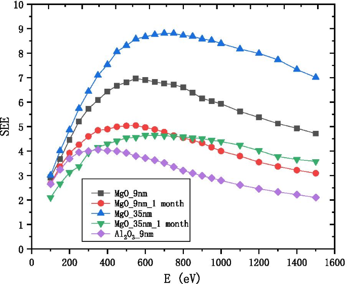
9 nm-Al2O3、9 nm-MgO和35 nm-MgO的SEE随入射电子能量的变化,以及样品在空气潮解1个月后测量的结果
已知潮解MgO的最终产物主要是Mg2(OH)2CO3和MgCO3,因此材料不同深度处C原子浓度的含量可以反映MgO的潮解深度。表面通过 Ar 离子束溅射蚀刻并通过 X 射线光电子能谱 (XPS) 进行分析。两者交替进行。通过控制蚀刻时间来控制蚀刻深度,通过XPS得到C和Mg元素的相对原子浓度百分比变化。当 XPS 无法测量 C 元素的相对浓度百分比时,此时的蚀刻深度为 MgO 的潮解深度。上述方法表明MgO的潮解深度约为3.8 nm,1 nm Al2O3可以保护MgO不被潮解。
为了测量材料的SEE水平,世界各地的许多实验室都建立了自己的专用测量装置,包括斯坦福直线加速器中心[14]、犹他大学[22]、普林斯顿大学[23]; ONERA/DESP [24];中国科学技术大学、西安交通大学、航天504研究所、中国散裂中子源、电子科技大学等我们设计了一个球面系统来测试材料的SEE水平,以确保全面收集二次电子,有助于提高测量结果的准确性。并且,我们建议使用低能二次电子代替低能电子束进行中和来测量绝缘材料的 SEE,例如 MgO 和 Al2O3,它避免了中和剂量和中和时间的缺点 [24, 25],这方法方便,成本低。
我们抱着盖房子的想法设计了电子倍增器的发射层,取得了很好的效果。我们比较邻居入射电子能量下的SEE值,以此为标准将材料划分为低能区、中能区和高能区。这与抑制微放电的领域不同[14]。发现中能区可以消除入射电子能量对SEE值的干扰。因此,选取中能区作为衡量材料SEE水平的标准,对Al2O3、MgO、MgO/Al2O3、Al2O3/MgO进行研究,得到经验公式。
目前提出的主要 SEE 物理模型是 Dionne 模型 [26, 27]。提出的双层模型[28]进一步修改,不适用于当前的实验数据。因此,我们建议使用过渡层的概念来解释多层材料,可以很好地解释设计的材料特性。
我们的实验和计算发现,在生长 Al2O3 然后生长 MgO 之后,当该薄膜比 MgO 薄膜更薄时,可以显示 MgO 的饱和 SEE 水平。解决了MgO薄膜过厚,导电层不能为发射层补充电荷的问题。并且我们发现在生长MgO然后生长Al2O3之后,3nm以上的Al2O3不再显示MgO的SEE水平; 1nm的Al2O3可以抵抗外界环境对MgO的破坏,长期保持MgO的SEE水平; 0.3 nm Al2O3 可以提高 MgO 的饱和 SEE 水平。因此,我们提出新发射层的制备工艺是在 2 nm Al2O3 缓冲层上生长 9 nm MgO 主层,然后在其上生长 1 nm Al2O3 保护层或 0.3 nm Al2O3 增强层,这样可以解决电子倍增器中发射层的MgO缺陷问题。我们通过在微通道板的微通道(一种电子倍增器)中生长这种新型发射层,大大提高了微通道板的增益。这种新型发射层的设计厚度对于提高电子倍增器的增益和稳定性具有重要意义。
实验和方法
使用原子层沉积的发射层
原子层沉积(ALD)是一种技术,它是前驱气体和反应气体以受控的速率交替进入基底表面,在表面发生物理或化学吸附或在表面发生表面饱和反应,沉积材料表面一层一层地形成单原子薄膜。 ALD可以生产连续的无针微通道薄膜,具有优良的覆盖率,并且可以控制原子薄膜的厚度和组成。因此,我们选择ALD作为研究发射层厚度的重要制备方法。
以下是使用ALD生长Al2O3的化学反应方程式:
$$\begin{aligned} {\text{A}} &:{\text{Substrate}} - {\text{OH}}^{*} + {\text{Al}}\left( {{\text {CH}}_{3} } \right)_{3} \to {\text{Substrate}} - {\text{O}} - {\text{Al}}\left( {{\text{CH }}_{3} } \right)_{2}^{*} + {\text{CH}}_{4} \uparrow \\ {\text{B}} &:{\text{Substrate}} - {\text{O}} - {\text{Al}}\left( {{\text{CH}}_{3} } \right)_{2}^{*} + 2{\text{H }}_{2} {\text{O}} \to {\text{Substrate}} - {\text{O}} - {\text{Al}}\left( {{\text{OH}}} \right)_{2}^{*} + 2{\text{CH}}_{4} \uparrow \\ {\text{C}} &:{\text{Al}} - {\text{OH }}^{*} + {\text{Al}}\left( {{\text{CH}}_{3} } \right)_{3} \to {\text{Al}} - {\text {O}} - {\text{Al}}\left( {{\text{CH}}_{3} } \right)_{2}^{*} + {\text{CH}}_{4 } \uparrow \\ {\text{D}} &:{\text{Al}} - {\text{CH}}_{3}^{*} + {\text{H}}_{2} { \text{O}} \to {\text{Al}} - {\text{OH}}^{*} + 2{\text{CH}}_{4} \uparrow \\ \end{aligned}$ $如 A 和 B 或 C 和 D 的方程式所示,基底表面最初覆盖有 –OH,–OH 与 Al(CH3)3 (TMA) 的化学反应形成新的 –CH3 表面,并释放出 CH4(副产物) )。新的–CH3 表面暴露在水蒸气中,它们的反应生成了新的–OH 表面并再次释放了CH4。反应温度为 200°C。生长一层Al2O3原子的时间和顺序如图2所示:
$${\text{TMA/N}}_{2} {\text{/H}}_{2} {\text{O/N}}_{2} =0.1\sim 1{\text{s }}/5\sim 45{\text{s}}/0.1\sim 1{\text{s }}/5\sim 45{\text{s}}{.}$$
Al2O3和MgO的生长过程示意图
以下是使用ALD生长MgO的化学反应方程式:
$$\begin{aligned} {\text{E}} &:{\text{Substrate}} - {\text{OH}}^{*} + {\text{Mg}}\left( {{\text {C}}_{5} {\text{H}}_{5} } \right)_{2} \to {\text{Substrate}} - {\text{O}} - {\text{MgC }}_{5} {\text{H}}_{5}^{*} + {\text{C}}_{5} {\text{H}}_{6} \uparrow \\ {\ text{F}} &:{\text{Substrate}} - {\text{O}} - {\text{MgC}}_{5} {\text{H}}_{5}^{*} + {\text{H}}_{2} {\text{O}} \to {\text{Substrate}} - {\text{OH}}^{*} + {\text{C}}_{5 } {\text{H}}_{6} \uparrow \\ {\text{G}} &:{\text{Mg}} - {\text{OH}}^{*} + {\text{Mg }}\left( {{\text{C}}_{5} {\text{H}}_{5} } \right)_{2} \to {\text{Mg}} - {\text{ O}} - {\text{MgC}}_{5} {\text{H}}_{5}^{*} + {\text{C}}_{5} {\text{H}}_ {6} \uparrow \\ {\text{H}} &:{\text{Mg}} - {\text{C}}_{5} {\text{H}}_{5}^{*} + {\text{H}}_{2} {\text{O}} \to {\text{Mg}} - {\text{OH}}^{*} + {\text{C}}_{ 5} {\text{H}}_{6} \uparrow \\ \end{aligned}$$如 E 和 F 或 G 和 H 的方程所示,基底表面最初覆盖着 \(- {\text{OH}}\), \(- {\text{OH}}\) 和\({\text{Mg}}\left( {{\text{C}}_{5} {\text{H}}_{5} } \right)_{2}\)(\({\ text{Mg}}\left( {{\text{C}}_{{\text{P}}} } \right)_{2}\)) 形成了新的 \(- {\text{C}} _{5} {\text{H}}_{5}\) 表面,并释放 \({\text{C}}_{5} {\text{H}}_{6}\) (副产品) .新的\(- {\text{C}}}_{5} {\text{H}}_{5}\) 表面暴露在水蒸气中,它们的反应产生了新的\(- {\text{OH}} \) 表面并再次释放 \({\text{C}}_{5} {\text{H}}_{6}\)。
我们在 60°C 下加热 \({\text{Mg}}\left( {{\text{C}}_{{\text{P}}} } \right)_{2}\) 将其变成灰尘。反应室的温度为 200°C。生长一层MgO原子的时间和顺序如图2所示:
$${\text{Mg}}\left( {{\text{Cp}}} \right)_{2} {\text{/N}}_{2} {\text{/H}}_{ 2} {\text{O/N}}_{2} =0.1\sim 1{\text{s}}/5\sim 45{\text{s}}/0.1\sim 1{\text{s } }/5\sim 45{\text{s}}{.}$$发射层的设计
样品以四种方式制备,如图 3 所示:在 Si 晶片上生长不同厚度的 \({\text{Al}}}_{2} {\text{O}}}_{3}\);在硅片上生长不同厚度的 MgO;在Si晶片上生长不同厚度的\({\text{Al}}_{2} {\text{O}}_{3}\),然后生长固定厚度的MgO;在 Si 晶片上生长固定厚度的 MgO,然后生长不同厚度的 \({\text{Al}}}_{2} {\text{O}}_{3}\)。我们在硅晶片上生长了不同厚度的 \({\text{Al}}_{2} {\text{O}}_{3}\)(1 nm、3 nm、7 nm、9 nm、30 nm , 50 纳米)。我们在硅晶片上生长了不同厚度的 MgO(1 纳米、3 纳米、5 纳米、9 纳米、15 纳米、20 纳米、35 纳米)。我们在硅晶片(0.6 纳米、1 纳米、3 纳米、30 纳米)上生长不同厚度的 \({\text{Al}}_{2} {\text{O}}_{3}\) 然后生长MgO 的固定厚度(9 nm)。我们在 Si 晶片上生长固定厚度的 MgO(35 nm),然后生长不同厚度的 \({\text{Al}}}_{2} {\text{O} }_{3}\)(0.3 纳米、0.6 纳米、1 纳米、3 纳米、5 纳米、7 纳米、10 纳米、20 纳米)。
<图片>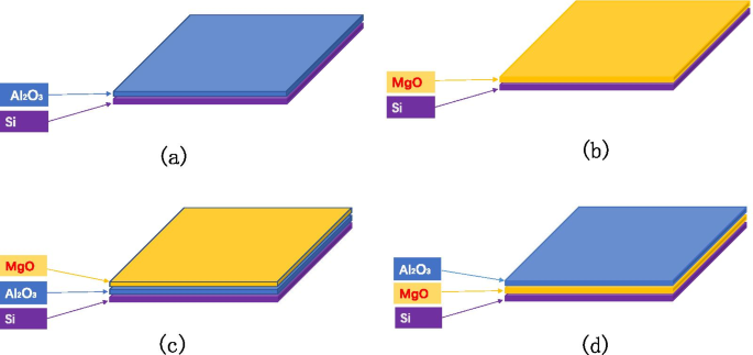
通过设计发射层实验研究薄膜厚度与SEE的关系
SEE 的新测试方法
我们使用收集器的方法进行测量,如图 4 所示:首先将样品台连接到收集器,皮安表测量的电流为入射电子电流,记为 \(I_{{\text{p}}}\ );在相同的入射条件下,断开样品和集电极,此时集电极上测得的电流为二次电子电流,记为\(I_{{\text{s}}}\)。
$${\text{SEE}} =\frac{{I_{{\text{s}}} }}{{I_{{\text{p}}} }}$$
二次电子发射效率系统示意图
我们将器件设计成球形结构,确保二次电子的充分收集,有助于提高测量结果的准确性。
当绝缘材料受到入射电子的轰击时,材料表面会放出二次电子,并因失去电子而积聚正电荷。正电荷使电位上升。因为二次电子是在距离材料表面几纳米的范围内产生的,并且具有低能量 (~ eV)。二次电子对正电位非常敏感。正电位会影响下一次的二次电子发射过程,导致二次电子产率下降。
为了消除电荷积累对绝缘样品SEE测量结果的影响,准确测量绝缘样品的SEE,传统方法直接采用低能电子束照射绝缘样品,正极样品表面的电荷被低能电子中和。传统方法有两个缺点。第一,需要准确计算中和剂量,容易中和剂量不足导致样品表面带正电荷,或中和过度导致样品表面带负电荷;其次,需要再配备1支低能电子枪[24, 25]。
我们建议使用低能二次电子代替低能电子束进行中和,克服了传统方法的缺点,获得了准确的二次电子,如图 5 [29] 所示。我们将要测试的绝缘样品放置在样品台的一半上,另一半留空。样品台由304不锈钢制成,电位为0 V。
<图片>材料二次电子发射系数新测试方法示意图
在测试绝缘样品时,电子枪产生的电子轰击绝缘样品的表面,如图 5a 所示,产生如图 5b 所示的正电荷区域。在中和绝缘样品的表面电荷时,通过调整电子枪的角度轰击样品台的半空区域,使样品台发射二次电子,如图5b所示。
由于正电荷和电子的相互吸引,二次电子被吸引到样品表面进行电荷中和。随着正电荷的减少,吸引的电子越少。当样品表面的正电荷被中和后,绝缘样品的表面又恢复到原来的状态。由于不带正电荷,不会继续吸引样品台产生的低能二次电子,因此不会出现过度中和导致样品表面带负电的情况。
我们使用的电子枪每次都在同一位置轰击样品表面,然后偏转相同的角度轰击样品台上的相同位置,如图6所示。由于长期的SEE测试过程,该位置在电子枪长时间轰击的样品台上变成了如图6所示的黑点。
<图片>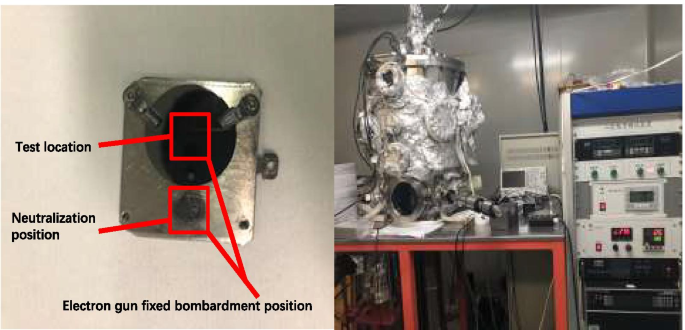
样品、样品台、二次电子发射系数测试设备照片
结果与讨论
查看分区和分析
我们比较相邻入射电子能量下的SEE值来描述SEE随入射电子能量的变化,定义为
$$R_{{{\text{SEE}}}} =\frac{{{\text{SEE}}\left( {x + b } \right)}}{{{\text{SEE}}\left ( {x } \right)}}$$并且材料的SEE被\(R_{{{\text{SEE}}}}\)值的大小分为三个区域,即入射电子的低能区(\(R_{{{ \text{SEE}}}} \ge 1.02\))、入射电子的中等能量区域 (\(0.98 \le R_{{{\text{SEE}}}} <1.02\)) 和高能量区域入射电子的区域 (\({\text{R}}_{{{\text{SEE}}}} \ge 0.98\))。我们用来测试 SEE 的材料的入射电子能量范围是 (100 eV, 1500 eV), x 表示入射电子能量,b 表示SEE测试中入射电子能量的步长。
\({\text{Al}}_{2} {\text{O}}_{3}\) SEE 在 7 nm 之后基本保持不变,如图 7 所示。如图 7a、b 所示, \({\text{Al}}_{2} {\text{O}}_{3}\) 的低能量区域在 100 到 250 eV 之间,\(R_{{{\text{SEE}} }}\) 从 1.25 降低到 1.02,表明随着入射电子能量的增加,SEE 增加并最终稳定。如图 7c、d 所示,\({\text{Al}}_{2} {\text{O}}_{3}\) 的中等能量区域在 250 到 500 eV 之间,\( R_{{{\text{SEE}}}}\) 在区间 [0.98, 1.02] 内被认为是常数,即\(R_{{{\text{SEE}}}}\) 近似相等到 1,表明随着入射电子能量的增加,SEE 基本不变。如图 7e、f 所示,\({\text{Al}}_{2} {\text{O}}_{3}\) 的高能量区域在 500 到 1500 eV 之间,每增加一次200 eV 的入射电子能量,SEE 降低约 0.9 倍。
<图片>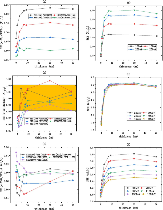
将入射电子能量除以 \(R_{{{\text{SEE}}}} =\frac{{\text{SEE(x + b)}}}{{\text{SEE(x)}}} \) 如 a 所示 , c , e Al2O3 (在硅片上,生长 xnm-Al2O3) SEE 随厚度的变化,如图 b , d , f
MgO SEE 在 20 nm 之后基本保持不变,如图 9 所示。如图 8a、b 所示,MgO 的低能量区域在 100 到 500 eV 之间,\(R_{{{\text{SEE} }}}\) 从 1.3 减小到 1,表明随着入射电子能量的增加,SEE 增加并最终趋于稳定。如图 8c、d 所示,MgO 的中等能量区域在 500 到 1000 eV 之间,\(R_{{{\text{SEE}}}}\) 在 [0.98, 1.02 的区间内被认为是恒定的],即\(R_{{{\text{SEE}}}}\)近似等于1,说明随着入射电子能量的增加,SEE基本不变。如图 8e、f 所示,MgO 的高能区在 1000 到 1500 eV 之间,入射电子能量每增加 100 eV,SEE 降低约 0.94 倍。
<图片>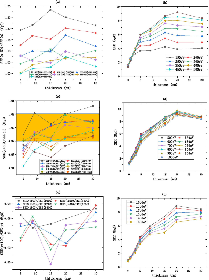
将入射电子能量除以 \(R_{{{\text{SEE}}}} =\frac{{\text{SEE(x + b)}}}{{\text{SEE(x)}}} \) 如 a 所示 , c , e MgO (在硅片上,生长 xnm-MgO) SEE 随厚度的变化,如图 b , d , f
如图 9 所示,\({\text{Al}}_{2} {\text{O}}_{3}\)/MgO 和 MgO 的 SEE 具有相似的入射电子能量分配,SEE \({\text{Al}}_{2} {\text{O}}_{3}\)/MgO 在 3 nm 后基本保持不变。如图 9a、b 所示,\({\text{Al}}_{2} {\text{O}}_{3}\)/MgO 的低能量区域在 100 到 450 eV 之间, \(R_{{{\text{SEE}}}}\) 从 1.4 减小到 1.05,表明随着入射电子能量的增加,SEE 增加并最终趋于稳定。如图 9c、d 所示,\({\text{Al}}_{2} {\text{O}}_{3}\)/MgO 的中等能量区域在 500 到 1000 eV 之间, \(R_{{{\text{SEE}}}}\) 在 [0.98, 1.02] 的区间内被认为是常数,即 \(R_{{{\text{SEE}}}}\) 是约等于 1,说明随着入射电子能量的增加,SEE 基本不变。如图 9e、f 所示,\({\text{Al}}_{2} {\text{O}}_{3}\)/MgO 的高能区在 1000 到 1500 eV 之间,对于入射电子能量每增加 100 eV,SEE 就会降低约 0.95 倍。因为 \({\text{Al}}_{2} {\text{O}}_{3}\)/MgO 的 SEE 在中等能量区域是稳定的,所以可以将入射电子能量作为变量排除因素。
<图片>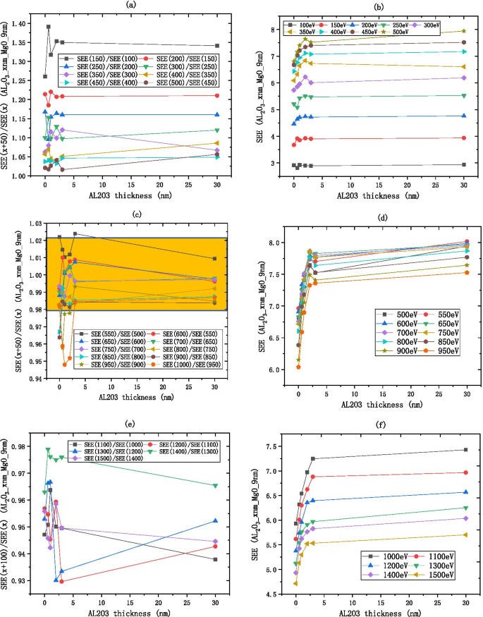
将入射电子能量除以 \(R_{{{\text{SEE}}}} =\frac{{\text{SEE(x + b)}}}{{\text{SEE(x)}}} \) 如 a 所示 , c , e Al2O3/MgO 的变化(在硅晶片上,生长 xnm-Al2O3,然后生长 9 nm-MgO)SEE 厚度如 b 所示 , d , f
如图 10 所示,MgO/\({\text{Al}}_{2} {\text{O}}_{3}\) 和 \({\text{Al}}_{ 2} {\text{O}}}_{3}\) 具有相似的入射电子能量分配,MgO/\({\text{Al}}}_{2} {\text{O}}_{3 }\) 在 3 nm 之后基本保持不变。如图 10a、b 所示,MgO/\({\text{Al}}_{2} {\text{O}}_{3}\) 的低能量区域在 100 到 300 eV 之间, \(R_{{{\text{SEE}}}}\) 从 1.8 减小到 1,表明随着入射电子能量的增加,SEE 增加并最终趋于稳定。如图 10c、d 所示,MgO/\({\text{Al}}_{2} {\text{O}}_{3}\) 的中等能量区域在 300 到 500 eV 之间, \(R_{{{\text{SEE}}}}\) 被认为是 [0.98, 1.02] 区间内的常数,当 \({\text{Al}}}_{2} {\text{O}} _{3}\)薄,\(R_{{{\text{SEE}}}}\)偏离1,不同入射电子能量下SEE差异明显;当 \({\text{Al}}_{2} {\text{O}}_{3}\) 厚时,\(R_{{{\text{SEE}}}}\) 接近于 1 ,而且差别并不明显。如图 10e、f 所示,MgO/\({\text{Al}}_{2} {\text{O}}_{3}\) 的高能区在 500 到 1500 eV 之间\({\text{Al}}}_{2} {\text{O}}_{3}\) 很薄,\(R_{{{\text{SEE}}}}\) 接近于 1,不同入射电子能量下SEE差异不明显;当 \({\text{Al}}}_{2} {\text{O}}_{3}\) 厚时, \(R_{{{\text{SEE}}}}\) 偏离 1,而且区别很明显;入射电子能量每增加 200 eV,SEE 降低约 0.9 倍。
<图片>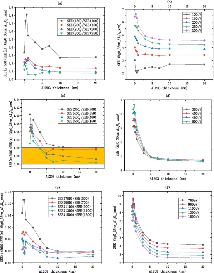
将入射电子能量除以 \(R_{{{\text{SEE}}}} =\frac{{\text{SEE(x + b)}}}{{\text{SEE(x)}}} \) 如a, c, e所示 , MgO/Al2O3 (在硅片上,生长 35 nm-MgO,然后生长 xnm-Al2O3) SEE 随厚度的变化,如图 b , d, f
因为 \({\text{Al}}_{2} {\text{O}}_{3}\) SEE 在中等能量区域是稳定的,所以可以排除入射电子能量作为可变因素。我们选择中等入射电子能量 300 eV 作为标准来测量 \({\text{Al}}_{2} {\text{O}}}_{3}\) 的 SEE 能级,其经验公式为\({\text{Al}}_{2} {\text{O}}_{3}\) 的厚度和最佳 SEE 是通过拟合获得的,如图 11a(表 1)所示。
$${\text{B}}\_{\text{SEE}}_{{{\text{Al}}_{2} {\text{O}}_{3} }} =3.99 - 2.5{ *}e^{{ - \frac{{{\text{thickness}}}}{1.73}}}$$ (1)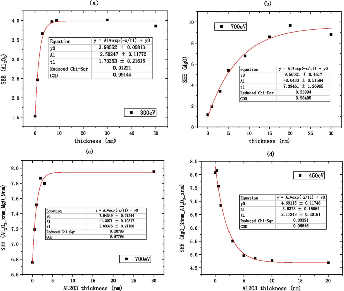
材料最佳二次电子发射系数与薄膜厚度的关系,a 显示Al2O3的信息(在硅片上,生长xnm-Al2O3),b 显示MgO的信息(在硅片上,生长xnm-MgO),c 显示了 Al2O3/MgO 的信息(在硅片上,生长 xnm-Al2O3,然后生长 9 nm-MgO),以及 d 显示 MgO/Al2O3 的信息(在硅片上,生长 35 nm-MgO,然后生长 xnm-Al2O3)
由于 MgO SEE 在中等能量区是稳定的,因此可以将入射电子能量作为可变因素排除在外。 We choose the medium incident electron energy 700 eV as the standard to measure the SEE level of MgO, the empirical formula for the thickness of alumina material and the best SEE is obtained by fitting as shown in Fig. 11b.
$${\text{B}}\_{\text{SEE}}_{{{\text{MgO}}}} =9.56 - 8.64*e^{{ - \frac{{{\text{thickness}}}}{7.39}}}$$ (2)Because the SEE of \({\text{Al}}_{2} {\text{O}}_{3} /{\text{MgO}}\) is stable in the medium energy region, the incident electron energy can be excluded as a variable factor. We choose the medium incident electron energy 700 eV as the standard to measure the SEE level of \({\text{Al}}_{2} {\text{O}}_{3}\)/MgO, the empirical formula for the thickness of alumina material and the best SEE is obtained by fitting as shown in Fig. 11c.
$${\text{B}}\_{\text{SEE}}_{{{\text{Al}}_{2} {\text{O}}_{3} /{\text{MgO}}}} =7.94 - 1.21\,*\,e^{{ - \frac{{{\text{thickness}}}}{1.03}}}$$ (3)Because the SEE of MgO/\({\text{Al}}_{2} {\text{O}}_{3}\) is stable in the medium energy region, the incident electron energy can be excluded as a variable factor. We choose the medium incident electron energy 450 eV as the standard to measure the SEE level of MgO/\({\text{Al}}_{2} {\text{O}}_{3}\), the empirical formula for the thickness of alumina material and the best SEE is obtained by fitting as shown in Fig. 11d.
$${\text{B}}\_{\text{SEE}}_{{{\text{MgO}}/{\text{Al}}_{2} {\text{O}}_{3} }} =4.69 + 3.64\,*\,e^{{ - \frac{{{\text{thickness}}}}{2.11}}}$$ (4) $$\frac{{{\text{B}}\_{\text{SEE}}_{{{\text{MgO}}}} \left( 9 \right)}}{{{\text{B}}\_{\text{SEE}}_{{{\text{Al}}_{2} {\text{O}}_{3} }} \left( {30} \right)}} =\frac{{9.56 - 8.64\,*\,e^{{ - \frac{9}{7.39}}} }}{{3.99 - 2.5\,*\,e^{{ - \frac{30}{{1.73}}}} }} \approx 1.755$$According to formulas 1 and 2, the SEE level of 9 nm MgO is 1.755 times higher than that of 30 nm \({\text{Al}}_{2} {\text{O}}_{3}\).
$$\begin{aligned} \frac{{{\text{B}}\_{\text{SEE}}_{{{\text{Al}}_{2} {\text{O}}_{3} /{\text{MgO}}}} \left( 3 \right)}}{{{\text{B}}\_{\text{SEE}}_{{{\text{Al}}_{2} {\text{O}}_{3} }} \left( {30} \right)}} &=\frac{{7.94 - 1.21\,*\,e^{{ - \frac{3}{{1.03}}}} }}{{3.99 - 2.5\,*\,e^{{ - \frac{{30}}{{1.73}}}} }} \approx 1.973 \\ \frac{{{\text{B}}\_{\text{SEE}}_{{{\text{Al}}_{2} {\text{O}}_{3} /{\text{MgO}}}} \left( 3 \right)}}{{{\text{B}}_{{{\text{SEE}}\,{\text{MgO}}}} \left( 9 \right)}} &=\frac{{7.94 - 1.21\,*\,e^{{ - \frac{3}{{1.03}}}} }}{{9.56 - 8.64\,*\,e^{{ - \frac{9}{{7.39}}}} }} \approx 1.124 \\ \end{aligned}$$We deposit 0–30 nm \({\text{Al}}_{2} {\text{O}}_{3}\) and redeposit 9 nm MgO on the Si wafer as the film, as shown in Fig. 12a. formulas 1 and 3 show that the SEE level of 9 nm MgO grown on 3 nm \({\text{Al}}_{2} {\text{O}}_{3}\) is 1.973 times higher than that of \({\text{Al}}_{2} {\text{O}}_{3}\). formulas 2 and 3 show that the SEE level of 9 nm MgO grown on 3 nm \({\text{Al}}_{2} {\text{O}}_{3}\) is 1.124 times higher than that of 9 nm MgO.
$$\frac{{{\text{B}}\_{\text{SEE}}_{{{\text{MgO}}/{\text{Al}}_{2} {\text{O}}_{3} }} }}{{{\text{B}}\_{\text{SEE}}_{{{\text{Al}}_{2} {\text{O}}_{3} }} }} =\frac{{4.69 + 3.64\,*\,e^{{ - \frac{1}{2.11}}} }}{{3.99 - 2.5\,*\,e^{{ - \frac{30}{{1.73}}}} }} \approx 1.743$$
Change of secondary electron emission coefficient with different incident electron energy, a shows the information of Al2O3/MgO (on the silicon wafer, grow xnm-Al2O3, and then grow 9 nm-MgO), b shows the information of MgO/Al2O3 and deliquescent MgO/Al2O3 (on the silicon wafer, grow 35 nm-MgO, and then grow 1 nm-Al2O3), c shows the information of MgO/Al2O3 (on the silicon wafer, grow 35 nm-MgO, and then grow 0.3 nm-Al2O3), and d shows the information of Al2O3/MgO (on the silicon wafer, grow 3 nm-Al2O3, and then grow 5 nm-MgO)
The SEE level of MgO after deliquescent drops significantly as shown in Fig. 1. Then, we deposit 35 nm MgO and redeposit 1 nm \({\text{Al}}_{2} {\text{O}}_{3}\) on the Si wafer as the film. We found the SEE of this film exposed to the air 7 months is close to the SEE without exposed to the air as shown in Fig. 12b. Formulas 1 and 3 show that the SEE level of 1 nm \({\text{Al}}_{2} {\text{O}}_{3}\) grown on MgO is 1.743 times higher than the SEE of \({\text{Al}}_{2} {\text{O}}_{3}\) and can be long-term maintain a high SEE level (no obvious deliquescence in 7 months).
$$\begin{aligned} \frac{{{\text{B}}\_{\text{SEE}}_{{{\text{MgO}}/{\text{Al}}_{2} {\text{O}}_{3} }} \left( {0.3} \right)}}{{{\text{B}}\_{\text{SEE}}_{{{\text{Al}}_{2} {\text{O}}_{3} }} \left( {30} \right)}} &=\frac{{4.69 + 3.64\,*\,e^{{ - \frac{0.3}{{2.11}}}} }}{{3.99 - 2.5\,*\,e^{{ - \frac{30}{{1.73}}}} }} \approx 1.967, \\ \frac{{{\text{B}}\_{\text{SEE}}_{{{\text{MgO}}/{\text{Al}}_{2} {\text{O}}_{3} }} \left( {0.3} \right)}}{{{\text{B}}\_{\text{SEE}}_{{{\text{MgO}}}} \left( 9 \right)}} &=\frac{{4.69 + 3.64\,*\,e^{{ - \frac{0.3}{{2.11}}}} }}{{9.56 - 8.64\,*\,e^{{ - \frac{9}{7.39}}} }} \approx 1.12 \\ \end{aligned}$$We deposited 35 nm MgO on the Si wafer and re-deposited 0.3 nm \({\text{Al}}_{2} {\text{O}}_{3}\) as a thin film as shown in Fig. 12c. It can be seen from formulas 1, 2 and 4 that the SEE level of 0.3 nm \({\text{Al}}_{2} {\text{O}}_{3}\) grown on MgO is 1.967 times higher than that of \({\text{Al}}_{2} {\text{O}}_{3}\) and 1.12 times higher than that of MgO;
The emission layer of the electron multiplier pursues thinner and higher SEE level, so we sacrificed some SEE level to make the film thinner. We deposited 3 nm \({\text{Al}}_{2} {\text{O}}_{3}\) on the Si wafer and re-deposited 5 nm MgO as a thin film as shown in Fig. 12d.
We propose to grow 2–3 nm \({\text{Al}}_{2} {\text{O}}_{3}\) as a buffer layer, grow 5–9 nm MgO as the main layer, and grow 0.3 nm \({\text{Al}}_{2} {\text{O}}_{3}\) as an enhancement layer or 1 nm \({\text{Al}}_{2} {\text{O}}_{3}\) as a protective layer as the \({\text{Al}}_{2} {\text{O}}_{3}\)/MgO/\({\text{Al}}_{2} {\text{O}}_{3}\) emissive layer of electron multipliers as shown in Fig. 13. SEE level of \({\text{Al}}_{2} {\text{O}}_{3}\)/MgO/\({\text{Al}}_{2} {\text{O}}_{3}\) emission layer (\({\text{Al}}_{2} {\text{O}}_{3}\)/MgO/\({\text{Al}}_{2} {\text{O}}_{3}\) = 3 nm/9 nm/0.3 nm) is shown in Fig. 12a. And, we tested a traditional microchannel plate with good gain and then grew \({\text{Al}}_{2} {\text{O}}_{3}\)/MgO/\({\text{Al}}_{2} {\text{O}}_{3}\) emission layer on microchannel wall of microchannel plate, and the gain result obtained by the test was significantly improved. Then, another piece of the first convention microchannel plate with close gain is grown with \({\text{Al}}_{2} {\text{O}}_{3}\) emission layer. Compared with the gain results obtained by the test, the \({\text{Al}}_{2} {\text{O}}_{3}\)/MgO/\({\text{Al}}_{2} {\text{O}}_{3}\) emission layer structure is more superior as shown in Fig. 14.

Schematic diagram of sandwich structure (Al2O3/MgO/Al2O3)

Relationship between the voltage and gain of the three microchannel plates (conventional microchannel plate, microchannel plate for growing Al2O3 emission layer, microchannel plate for growing Al2O3/MgO/Al2O3 emission layer)
XPS Characterization and Transition Layer Concept
SEE data usually uses Dionne model for fitting analysis [26, 27]. The current double-layer model based on Dionne model does not consider the existence of a transition layer between the two materials. Through the design of the emission layer structure this time, the SEE difference between \({\text{Al}}_{2} {\text{O}}_{3}\)/MgO and \({\text{Si}}\)/MgO can be clearly observed. Under the same SEE level, MgO exhibits a very large thickness difference. Sample (0.3 nm \({\text{Al}}_{2} {\text{O}}_{3}\) grown on MgO) can get a higher SEE than MgO. Sample (1 nm \({\text{Al}}_{2} {\text{O}}_{3}\) grown on MgO) maintain a high SEE level. The current double-layer model [28] can no longer explain the above phenomenon, so we put forward the concept of transition layer, there are two kinds of materials at the interface, forming two processes:the process of destroying the bottom material and the process of building the top material. The following are two X-ray photoelectron spectroscopy (XPS) test experiments to prove and the concept of transition layer to understand the SEE phenomenon of multilayer materials.
XPS test experiment 1:
First, the sample (0.3 nm \({\text{Al}}_{2} {\text{O}}_{3}\) grown on MgO) in the air for 1 year are tested for XPS as shown in Fig. 15a. We use an Ar ion gun to etch the surface of the material, and then test the various elements in the material by XPS. The two are alternately performed. The etching depth is controlled by controlling the etching time, and the relative atomic concentration percentage changes of various elements are obtained by XPS. Al element is almost undetectable after 8 s of etching as shown in Fig. 16a. The etching rate of \({\text{Al}}_{2} {\text{O}}_{3}\) is known, \({\text{Etching}}\,{\text{rate}}_{{{\text{Al}}_{2} {\text{O}}_{3} }} =0.7{\text{{\AA}/s}}\),
$$\begin{aligned} &{\text{Etching}}\_{\text{Thickness}}_{{{\text{Al}}_{2} {\text{O}}_{3} }} ={\text{Etching rate }}_{{{\text{Al}}_{2} {\text{O}}_{3} }} *{\text{Etching time}}_{{{\text{Al}}_{2} {\text{O}}_{3} }} =0.7\,{\text{{\AA}/s}}\,*\,8\,{\text{s}} =5.6{\text{\AA}} \\ &{\text{Cycle}}\_{\text{Thickness}}_{{{\text{Al}}_{2} {\text{O}}_{3} }} =1.29\,{\text{{\AA}/cycle}}\,*3\,{\text{cycle}} =3.87{\text{\AA}} \\ &{\text{Etching}}\_{\text{Thickness}}_{{{\text{Al}}_{2} {\text{O}}_{3} }}> {\text{Cycle}}\_{\text{Thickness}}_{{{\text{Al}}_{2} {\text{O}}_{3} }} \\ \end{aligned}$$
Schematic diagram of XPS test experiment sample, a shows the information of MgO/Al2O3 (on the silicon wafer, grow 35 nm-MgO, and then grow 0.3 nm-Al2O3), b shows the information of deliquescent MgO/Al2O3 (on the silicon wafer, grow 35 nm-MgO, and then grow 0.3 nm-Al2O3), c shows the information of deliquescent MgO (on the silicon wafer, grow 11 nm-MgO), d shows the information of deliquescent MgO/Al2O3 (on the silicon wafer, grow 35 nm-MgO, and then grow 1 nm-Al2O3)

Atomic concentration percentage of C, Al, Si elements relative to Mg element obtained by XPS. 一 Shows the Al element information of deliquescent MgO/Al2O3 (on the silicon wafer, grow 35 nm-MgO, and then grow 0.3 nm-Al2O3), a shows the C element information of deliquescent MgO/Al2O3 (on the silicon wafer, grow 35 nm-MgO, and then grow 0.3 nm-Al2O3), c shows the C element information of deliquescent MgO (on the silicon wafer, grow 11 nm-MgO), d shows the Si element information of deliquescent MgO (on the silicon wafer, grow 11 nm-MgO), e shows the C element information of deliquescent MgO/Al2O3 (on the silicon wafer, grow 35 nm-MgO, and then grow 1 nm-Al2O3). f shows the Al element information of deliquescent MgO/Al2O3 (on the silicon wafer, grow 35 nm-MgO, and then grow 1 nm-Al2O3)
Therefore, it shows that \({\text{Al}}_{2} {\text{O}}_{3}\) must exist in the MgO part, that is, \({\text{Al}}_{2} {\text{O}}_{3}\) destroys the lattice state of the MgO surface. \({\text{Al}}_{2} {\text{O}}_{3}\) forms a finite solid solution in MgO [30]. At this time, the experimentally measured SEE level increased. As we all know, the higher the SEE level, the better the insulation of the material. Due to the destruction of the surface lattice, the surface layer of MgO is more insulating, which further confirms the process of destroying the underlying material in the concept of the transition layer.
According to the results of the SEE experiment, the SEE level has dropped significantly. A small amount of \({\text{Al}}_{2} {\text{O}}_{3}\) in the top layer cannot protect the MgO in the bottom layer. MgO is still deliquescent in the air. The air contains \({\text{O}}_{2} ,{\text{H}}_{2} {\text{O}},{\text{CO}}_{2} ,{\text{CO}},{\text{N}}_{2}\), etc. When air enters MgO, the reaction of MgO and \({\text{CO}}_{2}\) and \({\text{H}}_{2} {\text{O}}\) proceeds at the same time.
$$\begin{aligned} &{\text{MgO}} + {\text{H}}_{2} {\text{O}} ={\text{Mg}}\left( {{\text{OH}}} \right)_{2} \\ &{\text{MgO}} + {\text{CO}}_{2} ={\text{MgCO}}_{3} \\ &{\text{Mg}}\left( {{\text{OH}}} \right)_{2} + {\text{CO}}_{2} \rightleftharpoons {\text{MgCO}}_{3} + {\text{H}}_{2} {\text{O}} \\ &2{\text{MgO}} + 2{\text{H}}_{2} {\text{O}} + {\text{CO}}_{2} ={\text{Mg}}_{2} \left( {{\text{OH}}} \right)_{2} {\text{CO}}_{3} \\ \end{aligned}$$The above four chemical reactions occur, the deliquescent reaction of air and MgO is mainly the reaction of MgO and \({\text{CO}}_{2}\) and \({\text{H}}_{2} {\text{O}}\) to produce \({\text{MgCO}}_{3}\) and \({\text{Mg}}_{2} \left( {{\text{OH}}} \right)_{2} {\text{CO}}_{3}\). As long as the prepared MgO is exposed to the air, \({\text{Mg}}\left( {{\text{OH}}} \right)_{2}\) will be produced. After being placed in the air for 28 days, \({\text{MgCO}}_{3}\) is the main product [31]. Because the tested MgO sample needs to be transferred to the SEE test equipment, the actual test is the SEE level of MgO–\({\text{Mg}}\left( {{\text{OH}}} \right)_{2}\). Main reason for the decrease in SEE level is the \({\text{Mg}}_{2} \left( {{\text{OH}}} \right)_{2} {\text{CO}}_{3}\) and MgCO3 produced by deliquescent. Therefore, when using XPS, C can be selected as the calibration element for the deliquescent depth of MgO in the air. As shown in Fig. 16b, after 8 s of etching, no Al content is detected, but C content is still detected, indicating that the MgO in the bottom layer continues to deliquesce and is not protected by a small amount of \({\text{Al}}_{2} {\text{O}}_{3}\) as shown in Fig. 15b.
XPS test experiment 2:
First, the MgO sample in the air for 1 year are tested for XPS. After 1 min of etching, there was almost no C element as shown in Fig. 16c, indicating that the thickness of the dense \({\text{Mg}}_{2} \left( {{\text{OH}}} \right)_{2} {\text{CO}}_{3}\) film formed was the thickness of 1 min of etching.
After etching for 3 min, the sample begins to show Si element as shown in Fig. 16d, the etching rate of MgO and the thickness of \({\text{Mg}}_{2} \left( {{\text{OH}}} \right)_{2} {\text{CO}}_{3}\) film can be calculated through these data.
$$\begin{aligned} &{\text{Etching rate }}_{{{\text{MgO}}}} =\frac{{{\text{Thickness}}_{{{\text{MgO}}}} }}{{{\text{Etching time}}_{{{\text{MgO}}}} }} =\frac{{11.58\,{\text{nm}}}}{{180\,{\text{s}}}} =0.643{\text{{\AA}/s}} \\ &{\text{Etching}}\_{\text{Thickness}}_{{{\text{Mg}}_{2} \left( {{\text{OH}}} \right)_{2} {\text{CO}}_{3} }} \approx {\text{Etching}}\_{\text{Thickness}}_{{{\text{MgO}}}} \\ &\quad ={\text{Etching rate }}_{{{\text{MgO}}}} \,*\,{\text{Etching time}}_{{{\text{MgO}}}} =0.643{\text{\AA}}/{\text{s*}}60\,{\text{s}} \approx 3.85\,{\text{nm}} \\ \end{aligned}$$The 3.85 nm \({\text{Mg}}_{2} \left( {{\text{OH}}} \right)_{2} {\text{CO}}_{3}\) film layer acts as an air barrier layer to prevent further deliquescent of deep MgO as shown in Fig. 15c.
When 1 nm \({\text{Al}}_{2} {\text{O}}_{3}\) is grown on MgO, the XPS test data show that there is basically no C content and no Al content in the sample after the etching time of 14 s as shown in Fig. 16e, f.
$${\text{Etching}}\_{\text{Thickness}}_{{{\text{Al}}_{2} {\text{O}}_{3} }} ={\text{Etching rate }}_{{{\text{Al}}_{2} {\text{O}}_{3} }}* {\text{Etching time}}_{{{\text{Al}}_{2} {\text{O}}_{3} }} =0.7\,{\text{{\AA}/s}}\,*\,14\,{\text{s}} =9.8{\text{\AA}}$$It can be known by testing the C content that the depth of air penetration into the material is about 1 nm at this time. According to the concept of the transition layer, there are two kinds of materials at the interface to form the process of destroying the bottom layer material and constructing the top layer material. At the interface, \({\text{Al}}_{2} {\text{O}}_{3}\) destroys the crystal lattice on the surface of MgO. In order to prevent excessive infiltration of air, a complete \({\text{Al}}_{2} {\text{O}}_{3}\) atomic level is formed at least at 1 nm. When a complete \({\text{Al}}_{2} {\text{O}}_{3}\) atomic layer is not formed, the infiltration of air into the material cannot be prevented as in Example 1 above. The \({\text{Al}}_{2} {\text{O}}_{3}\) and \({\text{ Mg}}_{2} \left( {{\text{OH}}} \right)_{2} {\text{CO}}_{3}\) in the inner layer are mixed to help MgO form a dense air barrier layer in advance as shown in Fig. 15d.
The concept of transition layer understands the SEE phenomenon of multilayer materials:
The schematic diagram shown in Fig. 17a shows the concept of the transition layer, The thickness of the top layer material is \(d_{1}\), the thickness of the bottom layer material is \(d_{2}\) and the thickness of the transition layer is \(d_{1\sim 2}\).The schematic diagram is shown in Fig. 17b, c when there is enough thick \({\text{Al}}_{2} {\text{O}}_{3}\) or MgO, the incident electron depth is \(d_{{{\text{max}}\_1}}\), and there is no transition layer between \({\text{Al}}_{2} {\text{O}}_{3}\) and \({\text{Al}}_{2} {\text{O}}_{3}\) (there is no transition layer between MgO and MgO), that is, the thickness of the transition layer is 0. Through XPS test experiment 2, we get that the thickness of the transition layer between MgO and \({\text{Al}}_{2} {\text{O}}_{3}\) is 1 nm as shown in Fig. 17d, e.

一 Schematic diagram of the transition layer of the double layer structure, b schematic diagram of the Al2O3 transition layer and incident electron depth, c schematic diagram of the MgO transition layer and incident electron depth, d schematic diagram of the Al2O3/MgO transition layer, e schematic diagram of the MgO/Al2O3 transition layer
When the top layer material in the double-layer structure is MgO, the thickness of the MgO that reaches the saturated SEE level is different when the bottom layer material is different. If electrons are incident on the bottom layer material, the SEE level of the bottom layer material is low and cannot reach the saturated SEE level. Therefore, to reach the saturation SEE level, a complete MgO incident electron path needs to be formed. When the bottom layer material is different, such as Si or \({\text{Al}}_{2} {\text{O}}_{3}\), the thickness of the transition layer will be different, so the top layer MgO shows a different thickness.
It is found through experiments that a sample that grows 2 nm \({\text{Al}}_{2} {\text{O}}_{3}\) on a Si wafer and then grows 15 nm MgO can reach the SEE level of MgO saturation. Knowing that the thickness of the MgO–\({\text{Al}}_{2} {\text{O}}_{3}\) transition layer is 1 nm, it can be inferred that the thickness of the \({\text{Al}}_{2} {\text{O}}_{3}\)–Si transition layer is 1 nm, and the maximum depth of incident electrons of MgO is 14 nm as shown in Fig. 18a. It is found through experiments that the sample of 20 nm MgO grown on the Si wafer can reach the SEE level of MgO saturation. It has been inferred that the maximum depth of incident electrons of MgO is 14 nm, so the thickness of the MgO–Si transition layer can be calculated to be 6 nm as shown in Fig. 18b. Therefore, it can be explained that the SEE level of growing 2 nm \({\text{Al}}_{2} {\text{O}}_{3}\) on Si wafer and then growing 9 nm MgO is higher than the SEE level of 9 nm MgO growing on Si wafer. This is because the thickness of the MgO–\({\text{Al}}_{2} {\text{O}}_{3}\) transition layer is thinner than that of the MgO–Si transition layer. The actual MgO thickness of 8 nm involved in incident electrons is much thicker than 3 nm as shown in Fig. 18c, d.

Schematic diagram of the thickness of each layer of a multilayer structure, a shows the thickness of Al2O3/MgO (on the silicon wafer, grow 2 nm-Al2O3, and then grow 15 nm-MgO), b shows the thickness of MgO (on the silicon wafer, grow 20 nm-MgO), c shows the thickness of Al2O3/MgO (on the silicon wafer, grow 2 nm-Al2O3, and then grow 9 nm-MgO), d shows the thickness of MgO (on the silicon wafer, grow 9 nm-MgO)
It can be seen through experiments that growing 7 nm \({\text{Al}}_{2} {\text{O}}_{3}\) on Si wafers can reach the SEE level of \({\text{Al}}_{2} {\text{O}}_{3}\) saturation, so it can be calculated that the maximum depth of incident electrons of \({\text{Al}}_{2} {\text{O}}_{3}\) is 6 nm; growing 7 nm \({\text{Al}}_{2} {\text{O}}_{3}\) on 35 nm MgO can reach the SEE level of \({\text{Al}}_{2} {\text{O}}_{3}\) saturation, the thickness of the MgO-\({\text{Al}}_{2} {\text{O}}_{3}\) transition layer is 1 nm, and the maximum depth of incident electrons of \({\text{Al}}_{2} {\text{O}}_{3}\) is calculated again to be confirmed by 6 nm, as shown in Fig. 19a, b.

Schematic diagram of the thickness of each layer of a multilayer structure, a shows the thickness of Al2O3 (on the silicon wafer, grow 7 nm-Al2O3), b shows the thickness of MgO/Al2O3 (on the silicon wafer, grow 20 nm-MgO, and then grow 7 nm-Al2O3)
Conclusions
In conclusion, we designed a global-shaped structure device for testing the SEE of the material and propose to use low-energy secondary electrons instead of low-energy electron beam for neutralization to measure the insulating material. We designed the emission layer of the electron multiplier with the idea of building a house to study the relationship between \({\text{Al}}_{2} {\text{O}}_{3}\) and MgO. We propose the nearest neighbor SEE ratio and use this to divide the SEE incident electron energy of the material into the high-energy region, the middle-energy region and the low-energy region. We have obtained four empirical formulas for SEE and thickness by studying \({\text{Al}}_{2} {\text{O}}_{3}\), MgO, MgO/\({\text{Al}}_{2} {\text{O}}_{3}\),\({\text{ Al}}_{2} {\text{O}}_{3}\)/MgO. We propose to use the concept of transition layer for SEE interpretation of multilayer materials and obtained the optimal \({\text{Al}}_{2} {\text{O}}_{3}\)/MgO/\({\text{Al}}_{2} {\text{O}}_{3}\) three-layer structure thickness suitable for electron multiplier through formula analysis and experimental experience. The thin film with this structure can maintain a high SEE level for a long time. This new emission layer will have broad application prospects in the channel electron multiplier (CEM), microchannel plate (MCP), independent electron multiplier and other devices.
Availability of data and materials
The authors do not wish to share their data. Because the authors have academic competition with other institutions. The authors want to protect their academic achievements and seek research funding for future research.
纳米材料