电阻式随机存取存储器 (RRAM):材料、开关机制、性能、多级单元 (mlc) 存储、建模和应用概述
摘要
在这份手稿中,电阻随机存取存储器 (RRAM) 技术领域的最新进展被认为是最杰出的新兴存储器技术之一,因为它具有高速、低成本、增强的存储密度、在各个领域的潜在应用以及出色的性能。可扩展性进行了全面审查。首先,提供了新兴存储器技术领域的简要概述。讨论了 RRAM 的材料特性、电阻切换机制和电气特性。此外,还详细阐述了各种问题,例如耐久性、保持性、均匀性以及工作温度和随机电报噪声 (RTN) 的影响。讨论了 RRAM 的多级单元 (MLC) 存储能力,这对于实现更高的存储密度和低成本具有吸引力。已经提供了不同的操作方案来实现可靠的 MLC 操作及其物理机制。此外,这项工作还详细描述了各种流行 RRAM 模型的开关方法和电流电压关系。简要介绍了 RRAM 在安全、神经形态计算和非易失性逻辑系统等各个领域的预期应用。本综述文章最后讨论了 RRAM 的挑战和未来前景。
介绍
称为 RAM 的随机存取存储器可以是易失性或非易失性的。与动态随机存取存储器 (DRAM) 和静态随机存取存储器 (SRAM) 一样,易失性存储器在移除电源时会丢失其先前存储的数据。对于非易失性存储器,即使在移除电源后,先前存储的内容仍将继续保留。闪存是非易失性存储器的典型例子。内存技术结合了优点和缺点以实现更高的性能,例如计算机系统中使用的 DRAM 具有高容量和密度,但它们是易失性的,这意味着需要每隔几毫秒刷新一次。由于这种刷新,设备的能量消耗增加,这是不希望的。另一方面,SRAM 速度快,但也像 DRAM 一样易失;此外,SRAM 单元的尺寸较大,这阻碍了其大规模实施。闪存主要由金属氧化物半导体场效应晶体管 (MOSFET) 和每个存储单元中的浮动栅极组成,由于其低成本和高密度,目前正被广泛使用,特别是用于嵌入式应用.根据存储单元的组织方式,闪存分为 NOR 闪存和 NAND 闪存 [1]。在 NOR 闪存中,单元被单独读取和编程,因为它们与位线并联。这类似于 CMOS NOR 门架构中晶体管的并联连接。对于 NAND 闪存,其架构类似于 CMOS NAND 门的架构,因为单元串联连接到位线。必须注意的是,与并联相比,串联消耗的空间更少,从而降低了 NAND Flash 的成本。然而,两种类型的闪存都存在运行速度低(写入/擦除时间:1 ms/0.1 ms)、耐久性有限(10 6 写入/擦除周期)和高写入电压(> 10 V)[2]。
上面提到的内存技术,即DRAM、SRAM和Flash,都是基于电荷存储的内存。 DRAM以电荷的形式在电容上存储信息,SRAM是基于交叉耦合反相器节点上的电荷存储,而Flash存储器技术则是利用晶体管的浮栅来存储电荷。所有这些现有的基于电荷存储的存储器技术目前都面临着缩小到 10 nm 节点或更高的挑战。这归因于纳米级存储电荷的损失,从而导致性能、可靠性和噪声容限的下降。此外,DRAM对大刷新动态功率的要求以及SRAM和DRAM的泄漏功率对未来存储器层次结构的设计提出了严峻挑战。
因此,一类新的存储器通常被称为新兴存储器技术,目前正在开发中,主要是在业界积极研究,旨在彻底改变现有的存储器层次结构 [3]。这些新兴的存储器技术旨在将SRAM的开关速度、可与DRAM媲美的存储密度以及Flash存储器的非易失性结合起来,从而成为未来存储器层次结构中非常有吸引力的替代方案。
将存储设备归类为理想的存储设备,它应该具有以下特性:低工作电压(<1 V)、长循环寿命(>10 17 周期)、增强的数据保留时间(>10 年)、低能耗(fJ/bit)和卓越的可扩展性(<10 nm)[4]。然而,迄今为止,还没有满足这些理想特征的单一存储器。正在积极研究各种新兴的存储器技术,以满足这些理想存储器特性的一部分。这些依赖于电阻变化而不是电荷来存储信息的存储技术如下:(i)相变存储器(PCM),(ii)自旋转移矩磁阻随机存取存储器(STT-MRAM),以及( iii) 电阻式随机存取存储器 (RRAM)。在相变存储器中,开关介质由硫属化物材料(通常是 Ge2-Sb2-Te5,GST)组成 [5-7]。 PCM 依靠结晶相和非晶相之间的电阻差异来实现高效的数据存储能力。结晶相表示器件的低电阻状态 (LRS) 或导通状态,而非晶相表示高电阻状态 (HRS) 或关断状态。 SET 操作对应于 LRS,通常是指在设备中存储逻辑值“1”,而 RESET 操作对应于 HRS 存储逻辑值“0”。对于 SET 操作,PCM 在施加电压脉冲时被加热到其结晶温度以上,而对于 RESET 操作,更大的电流通过电池,然后突然切断以熔化然后淬火材料,以便达到非晶态。
在自旋转移矩磁阻随机存取存储器中,存储能力是由于磁隧道结 (MJT) [8-10],它由两个铁磁层和夹在它们之间的隧道电介质组成。参考层的磁方向是固定的,而施加外部电磁场可以改变自由铁磁层的磁方向。如果参考层和自由层具有相同的磁化方向,则 MTJ 被称为在 LRS 中。对于 MTJ,要在 HRS 中,两个铁磁层的磁化方向是反平行的。 RRAM 由夹在两个金属 (M) 电极之间的绝缘层 (I) 组成 [11, 12]。 RRAM依赖于两个电极之间的绝缘体中分别对应于LRS和HRS的导电细丝的形成和断裂[13-15]。
现有和新兴存储器技术的详细比较如表 1 所示。从表中可以明显看出,与 SRAM 相比,STT-MRAM 和 PCM 具有面积更小的优势。虽然 STT-MRAM 提供快速的写入/读取速度、长寿命和低编程电压,但另一方面,PCM 具有写入延迟大的缺点。与闪存相比,RRAM 具有更低的编程电压和更快的写入/读取速度,被视为闪存的潜在替代品。在所有新兴的存储器技术候选中,RRAM 具有显着的优势,例如易于制造、金属-绝缘体-金属 (MIM) 结构、出色的可扩展性、纳秒级速度、长数据保留以及与当前 CMOS 技术的兼容性,从而提供了具有竞争力的未来数字记忆的解决方案 [16]。 RRAM 最显着的优势如图 1 所示。
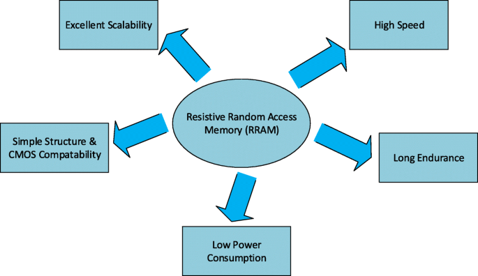
RRAM的优点
<图>在这项工作中,介绍了 RRAM 技术的最新进展和详细概述。 “电阻式随机存取存储器 (RRAM)”部分讨论了开关材料的回顾以及开关模式的分类和开关机制的细节。 “电阻式随机存取存储器 (RRAM) 的性能指标”部分重点介绍了 RRAM 的各种性能指标。 “多级电阻式随机存取存储器 (RRAM)”部分分析了 RRAM 的多级单元 (MLC) 特性以及各种 MLC 操作方案及其物理机制。 “RRAM 器件的建模”部分详细讨论了 RRAM 器件的建模。在“RRAM 的应用”部分讨论了 RRAM 的各种应用。最后,“挑战和未来展望”部分介绍了 RRAM 的挑战和未来展望。图 2 展示了在准备这篇评论手稿时参考的论文的类别分布。
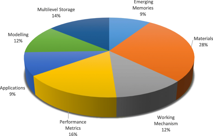
为准备 RRAM 审查而咨询的论文的类别分布
电阻随机存取存储器 (RRAM)
电阻转换材料
已经观察到,在一些绝缘体中,在施加电场的情况下会发生电阻的变化。最近研究了这种电阻变化的特性,以开发未来的非易失性存储器 [17]。已经在多种氧化物中观察到了电阻切换现象,但二元金属氧化物作为未来非易失性存储器应用的首选开关材料已被广泛研究,主要是因为它们与 CMOS BEOL 工艺兼容。表现出非挥发性电阻转换的各种金属氧化物基材料,例如氧化铪 (HfO x ) [18–23], 氧化钛 (TiO x ) [24–31], 氧化钽 (TaO x ) [32–36]、氧化镍 (NiO) [37–40]、氧化锌 (ZnO) [41–46]、钛酸锌 (Zn2TiO4) [47]、氧化锰 (MnO x ) [48, 49], 氧化镁 (MgO) [50], 氧化铝 (Al2O x ) [51-53] 和二氧化锆 (ZrO2) [54-58] 引起了最多的关注,并在过去几年中得到了广泛的研究。这些金属氧化物通常通过脉冲激光沉积 (PLD)、原子层沉积 (ALD) 和反应溅射来沉积。然而,ALD 是一种广泛优选的方法,因为它能够精确控制薄膜的厚度和均匀性 [59]。
在传统的电子设备中,电极材料的选择很重要,因为它们充当载流子的传输路径。对于 RRAM,电极材料的选择极大地影响了器件的开关行为。例如,在铜/聚(3-己基噻吩):[6,6]-苯基-C61-丁酸甲酯/氧化铟锡(Cu/P3HT:PCBM/ITO)结构中,观察到稳定的阻变行为;然而,在用铂电极代替铜电极后,它消失了[60]。多种材料已被用作 RRAM 的电极。电极材料按其组成可分为五类,包括单质电极、硅基电极、合金电极、氧化物电极和亚硝酸盐基电极。最丰富和最常用的电极是单质电极,包括 Al [51]、Ti[49]、Cu[30]、石墨烯 [61]、碳纳米管 [62]、Ag [41]、W [36]、和铂 [44]。对于硅基电极,p 型 Si 和 n 型 Si [63] 是唯一使用的电极类型。合金电极通常稳定电阻开关行为,主要包括Cu-Ti[64]、Cu-Te[65]和Pt-Al[66]。最常见的氮化物基电极是 TiN 和 TaN [67, 68]。氧化物基电极较为丰富,包括Al掺杂ZnO[69]、Ga掺杂ZnO[70]和ITO[71]。
最近在 RRAM 器件制造中使用的金属氧化物材料列表以及用于顶部电极和底部电极的各种材料组合如表 2 所示。还提供了各种参数的详细比较。从所使用的各种材料中,可以预测在各种类型的氧化物中广泛观察到非易失性电阻切换。用于制造 RRAM 的材料选择使其具有优势,因为金属氧化物金属 (MOM) 结构可以通过使用目前在半导体技术中使用的氧化物轻松制造。 RRAM中的底部电极材料通常是铂,有点难以蚀刻。对于单个器件结构,RRAM 可以共享相同的底部电极,而对于交叉架构,每个器件使用单独的底部电极。它们可以通过物理气相沉积和剥离依次获得。顶部电极和电阻开关层采用原子层沉积(ALD)或物理气相沉积(PVD)沉积。
<图>电阻切换模式
电阻式随机存取存储器 (RRAM) 由具有金属-绝缘体-金属结构的电阻式开关存储单元组成,通常称为 MIM 结构。该结构包括夹在两个金属 (M) 电极之间的绝缘层 (I)。 RRAM单元的示意图和截面图分别如图3a和b所示。
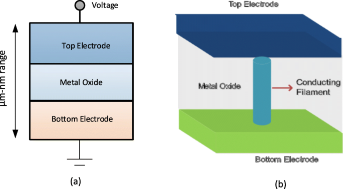
一 RRAM 的金属-绝缘体-金属结构示意图。 b RRAM剖面图
跨 RRAM 单元施加外部电压脉冲使器件能够从高电阻状态 (HRS) 或通常称为逻辑值“0”的关闭状态转变为低电阻状态 (LRS),或通常称为开启状态称为逻辑值“1”,反之亦然。电阻开关 (RS) 现象被认为是 RRAM 单元中电阻值发生这种变化的原因。准备好的 RRAM 最初处于高电阻状态 (HRS),为了将器件从 HRS 切换到 LRS,高压脉冲的应用能够在切换层中形成导电路径,并且 RRAM 单元被切换进入 LRS [72]。由于金属绝缘体金属 (MIM) 结构的软击穿而发生的这一过程通常称为“电铸”,而发生此过程的电压称为形成电压 (V f )。必须注意的是,发现形成电压取决于单元面积 [73] 和氧化物厚度 [74]。现在,要将 RRAM 单元从 LRS 切换到 HRS,电压脉冲称为 RESET 电压 (V 应用复位)以启用此切换转换,并且该过程被称为“复位”过程[75-78]。 RRAM 的 HRS 可以在施加电压脉冲时更改为 LRS。从 HRS 转变为 LRS 的电压称为 SET 电压 (V set),这个过程被称为“SET”过程[79]。为了有效地从 RRAM 单元读取数据,施加不会干扰单元当前状态的小的读取电压来确定单元是处于逻辑 0 (HRS) 还是逻辑 1 (LRS) 状态。由于即使去除施加的电压后 LRS 和 HRS 仍保留其各自的值,因此 RRAM 是一种非易失性存储器。根据施加电压的极性,RRAM 可以分为两种类型的开关模式:(i)单极开关和(ii)双极开关 [80]。在单极切换中,器件在各种电阻状态之间的切换(设置和复位过程)不依赖于所施加电压的极性,即切换可以在施加相同极性但大小不同的电压时发生,如图 1 所示。 4a.另一方面,在双极切换中,器件在各种电阻状态之间的切换(设置和复位过程)取决于施加电压的极性,即从 HRS 到 LRS 的转变发生在一个极性(正极或负)和相反的极性将 RRAM 单元切换回 HRS,如图 4b 所示。在单极开关中,焦耳热被解释为负责在复位操作期间使导电灯丝破裂的物理机制。另一方面,在双极开关中,带电物质的迁移是导电丝溶解的主要驱动力,尽管焦耳热仍然有助于加速迁移。为了保证在 RRAM 的形成/设置过程中,介质开关层没有永久击穿,顺从电流 (I cc) 对 RRAM 设备强制执行。顺从电流 (I cc) 在片外测试时通常由电池选择装置(晶体管、二极管、电阻器)或半导体参数分析仪来保证。
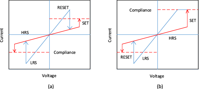
RRAM 的 I-V 曲线。 一 单极开关和b 双极开关[4]
阻变机制
RRAM 单元的切换基于电介质内导电丝 (CF) 的生长。 CF是具有纳米数量级的非常小的直径的通道,其连接存储单元的顶部和底部电极。当灯丝连接时获得具有高导电性的低电阻状态 (LRS),当灯丝断开且电极之间有间隙时会产生高电阻 (HRS) [91]。根据导电细丝的组成,RRAM 可分为以下两种类型:(i) 金属离子型 RRAM 也称为导电桥随机存取存储器 (CBRAM) 和 (ii) 氧空位细丝型 RRAM 称为作为'OxRRAM'。这里必须注意的是,CBRAM 有时被称为电化学金属化存储器 (ECM),而“OxRRAM”有时也称为价变存储器 (VCM)。
在基于金属离子的 RRAM 也称为“CBRAM”中,负责电阻转换的物理机制基于金属离子的迁移和随后的还原/氧化(氧化还原)反应 [92, 93]。 CBRAM 结构包括一个可氧化的顶部电极(阳极),例如 Ag、Cu 和 Ni,一个相对惰性的底部电极(阴极),例如W、Pt 和夹在两个电极之间的金属氧化物层。由于活性金属电极(最常见的是 Ag 或 Cu)的溶解、阳离子(Cu + 或 Ag + ),以及它们随后在惰性底部电极上的沉积或还原 [94]。因此,这种类型的RRAM的电阻开关行为由金属细丝的形成和溶解决定。
为了更好地理解基于金属离子的 CBRAM 的开关机制,让我们考虑一个 Ag/a-ZnO/Pt RRAM 单元的例子 [41]。描绘导电桥式随机存取存储器单元的切换过程的一般示意图如图 5 所示。CBRAM 存储器单元的原始状态如图 5a 所示。 Ag 顶部电极 (TE) 是形成灯丝的活性成分,而底部 Pt 电极是惰性的。在对 Ag 顶部电极施加正偏压时,氧化 (Ag → Ag + + e − ) 发生在顶部电极,因为 Ag + 生成阳离子并从 Ag 电极沉积到介电层 (a-ZnO) 中。 Pt 底部电极 (BE) 上的负偏压吸引 Ag + 阳离子,因此,还原反应 (Ag + + e − → Ag) 出现在底部电极处。因此,Ag + 阳离子被还原为 Ag 原子并积累直到形成导电桥(图 5b-d)并且据说 RRAM 器件表现出 LRS。这个过程被称为“SET”。当施加电压的极性反转时,高导电灯丝几乎完全溶解,设备被称为处于高电阻状态 (HRS)。这个过程被称为“RESET”,如图 5e 所示。
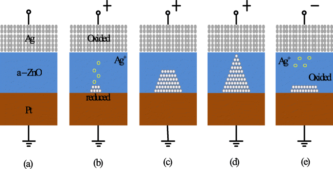
导电桥RRAM的开关机制示意图。 一 RRAM 设备的原始状态。 b , c Ag的氧化和Ag的迁移 + 向阴极的阳离子及其还原。 d Ag 原子和 Pt 电极的积累导致高导电丝的生长。 e 灯丝溶解发生在施加相反极性的电压[41]
在基于氧空位的 RRAM (OxRRAM) 中,负责电阻转换的物理机制通常与氧空位 (V \(_{o}^{2+}\)) 和随后氧离子的重新定位(O 2− ),从而能够在 RRAM 单元的顶部和底部电极之间形成导电细丝 [59]。最初,对于制造的 RRAM 单元,形成过程,即电介质的软击穿是必不可少的。一旦发生软介质击穿,在向阳极界面施加高电场时,氧原子被敲出晶格,变成氧离子(O 2− ) 而氧空位 (V \(_{o}^{2+}\)) 留在氧化层中。氧离子 (O 2− ) 与阳极材料反应或作为中性非晶格氧放电,如果贵金属用作阳极材料以形成界面氧化物层。因此,电极/氧化物界面就像一个“氧气库”[85]。接下来,氧空位的积累(V 体氧化物中的 \(_{o}^{2+}\)) 将 RRAM 单元切换到低电阻状态 (LRS),因为形成导电丝 (CF) 并且器件中流过可观的电流。为了将器件切换回高电阻状态 (HRS),重置过程发生在此期间,氧离子 (O 2− ) 从阳极界面迁移回本体氧化物并与氧空位 (V \(_{o}^{2+}\)) 或氧化金属 CF 沉淀物,从而使灯丝部分破裂,从而将 RRAM 单元切换回 HRS。对于表现出单极开关机制的 RRAM 单元,氧离子 (O 2− ) 由焦耳加热电流热激活,因此由于浓度梯度,氧离子从界面或 CF 周围的区域扩散。此外,必须注意的是,单极开关 RRAM 需要相对较高的复位电流来提高 CF 周围的局部温度。另一方面,在双极开关 RRAM 中,氧离子 (O 2− ) 需要借助反向电场,因为界面层可能存在显着的扩散势垒,而纯热扩散是不够的。必须注意的是,CF 的部分破裂在这两种情况下都会发生,将 RRAM 单元切换到高电阻状态 (HRS)。这主要是由于氧空位的形成(V \(_{o}^{2+}\)) 和导致电子隧道间隙的不良区域。为了将器件切换回 LRS(SET 工艺),CF 会由于间隙区域的软击穿而重新连接电极。类似的设置/重置过程可以重复多个周期。
基于上述讨论,CBRAM 也称为电化学金属化存储器 (ECM),它依赖于具有电化学活性的金属电极,例如 Ag、Cu 或 Ni,以形成基于金属阳离子的 CF [95]。基于氧空位灯丝的 RRAM ‘OxRRAM’中的 CF 也称为价变存储器 (VCM),由氧空位缺陷而不是金属原子组成,这是由于存储材料本身内的阴离子迁移[96]。尽管详细讨论了“OxRRAM”和“CBRAM”的切换机制,但关于两种 RRAM 类型的切换机制仍存在一些争论 [97]。例如,CF 在设置过程中开始生长的位置和重置过程中断开的位置,以及这些氧空位/金属原子如何聚集形成 CF。 Ta/TaOx连续20个开关周期的电流-电压(I-V)特性 研究了基于 /Pt [98] 的 RRAM 结构,并观察到 LRS 和 HRS 在连续开关周期中的明显变化。因此,整体内存窗口会减少,从而降低整体 RRAM 性能。这种循环间电阻变化主要归因于CF的随机形成及其在置位和复位操作期间的破裂。
表 3 显示了基于各种操作参数的 OxRRAM 与 CBRAM 的比较 [81, 84, 86–88, 99, 100]。这种比较揭示了这些 RRAM 存储器类型在耐久性特性方面的显着差异。这种不同是因为 CBRAM 的导电丝主要由金属原子组成,与氧空位相比,金属原子相对更容易漂移和扩散,从而导致 CBRAM 与 OxRRAM 相比的保留时间和耐久性特性下降。虽然两种 RRAM 类型的切换机制不同,但两者之间有许多共同的特点。唯一显着的区别是 OxRRAM 的耐用性明显高于 CBRAM。
<图>电阻式随机存取存储器 (RRAM) 的性能指标
耐力
电阻式随机存取存储器涉及高电阻状态 (HRS) 和低电阻状态 (LRS) 之间的频繁转换。电阻状态之间的每个切换事件都可能导致永久性损坏并导致 RRAM 性能下降。因此,耐久性被定义为 RRAM 设备可以在 HRS 和 LRS 之间切换的次数,同时确保它们之间的可靠可区分比率 [101]。因此,耐久性测试确定在 HRS 和 LRS 不再可区分之前可以有效切换的最大置位/复位周期数。通过在电阻开关单元中执行一系列 I-V 扫描并随后提取 R 来获得 RRAM 的耐用特性 HRS 和 R LRS 应用读取电压(通常为 0.1 V)[41]。这种方法是可靠的,因为可以在每个周期中获得设备的正确切换;然而,这种方法非常慢,因为获得 I-V 扫描所需的时间可能会非常长,尤其是在涉及较低电流的情况下。
H 中的耐久循环 f 哦 x RRAM 单元显示出对单元尺寸的强烈依赖,如图 6a 所示,其中报告了具有更大单元尺寸的 RRAM 器件具有更好的耐用性。此外,垂直减小层厚度会导致 2.5 V SET 电压的耐久性性能下降,如图 6b [102] 所示。这种随着开关层尺寸缩小而导致的耐久性性能下降是有源区中离子数量减少的结果。 H f 哦 x 基于RRAM的10 6 的出色续航表现 在 30 nm 单元尺寸低于 0.18 μ 的 1 kb 阵列上循环 m技术和相同的如图6c所示[103]。通过添加额外的 A 层 l 哦 x 在底部电极 (BE) 上方,阵列稳定性可以进一步提高,因为 HRS 的读取干扰免疫力增加。对于 T 一 哦 x 基于 RRAM,在 Ta/Ta2O5/TiN RRAM 结构中观察到耐久性性能随着脉冲宽度和复位电压幅度的增加而降低 [105]。 Ta/Ta2O5/TiN RRAM 中 TiN 和 Ru 底部电极的比较表明,耐久性下降的主要原因是氧离子与 TiN 电极的反应。此外,提高了 10 9 通过将 Ta2O5 层降低到 3 nm [106] 并使用宽度 <5 ns 的三角脉冲,在类似的 RRAM 结构中无需验证即可获得开关周期。大规模阵列性能,10 5 前后2-Mb Ta2O5内存对比 耐久性测试的循环如图 6d [104] 所示。电池电流分布显示初始和最终循环的微小变化。此外,LRS 的电池电流低于 50 μ A,表示阵列的低功耗。耐力高于10 12 的阻变器件 在涉及氧化钽 (TaO x ) 的交换媒体 [32, 36, 59]。 Thus, tantalum oxide-based RRAM devices seem to be exhibiting the highest endurance.
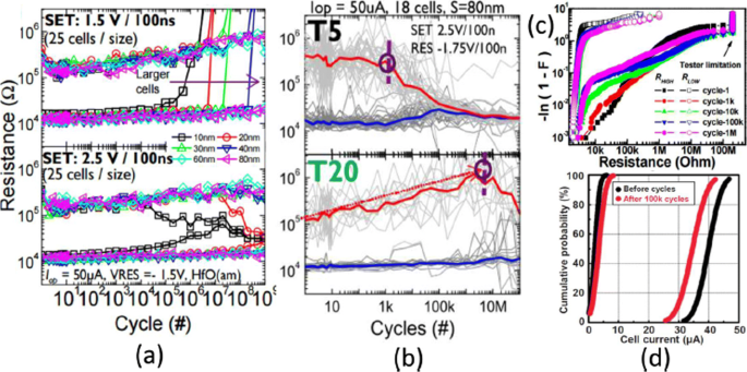
一 Endurance cycles of H f 哦 x -based RRAM at different SET voltage and cell size b with different thickness (T5=2 nm, T20=10 nm) at 2.5 V set voltage. c Resistance distribution of 1-kb array obtained from Weibull plots under different endurance cycles. d 100 k cycles endurance of 2-Mb-Ta2O5-based array; Reprinted from refs [102–104]
Retention
The data retention of a RRAM device involves investigating stability over a period of time for both LRS and HRS after undergoing set and reset transitions. In other words, the time period for which a memory cell will remain in a particular state after the set/reset operation determines the capability of a memory cell to retain its content [11]. The application of the constant voltage stress (CVS) over time using a low read voltage (0.1 V) and the measurement of the current versus time (I-t) curve for both LRS as well as the HRS enables the measurement of state retention. Due to the dispersing nature of atomic rearrangements induced in RRAM because of set voltage, the long retention time in LRS is difficult to obtain whereas, in HRS, retention is not a concern as it is usually the natural state of the device and RRAM will continue to remain in this state if no bias (or low bias) is applied. The retention in the LRS depends on the compliance limit during the SET transition, e.g. in RRAMs based on conductive filament switching mechanism, the larger compliance current produces a stronger conducting filament which is more stable over time [28, 41], as compared to a smaller compliance current. A projected endurance of 10 years at 85 ∘ C has been demonstrated in Ti/HfO2/TiN [18]. A commonly used method to obtain device endurance is by applying read pulse at high temperature after certain time intervals (e.g. every 1 s) and extrapolate the resistance to a 10-year period. Although this method is easy to implement, it has certain limitations primarily due to the read voltage stress applied to the cell. An alternative method is to change the temperature and record the time until the device fails. Activation energy is extracted by plotting the Arrhenius plot and extrapolate down to the operating temperature. However, the limitation of this method is that waiting is necessary until the failure occurs in the RRAM cell, and thus, this method is more time-consuming and expensive.
The device characteristics of H f 哦 x -based RRAM [81, 103] developed at the Industrial Technology Research Institute, Taiwan, are demonstrated to further understand the working of RRAM device. The transmission electron microscopy (TEM) image of the TiN/Ti/ H f 哦 x /TiN RRAM device with 30-nm cell size is shown in Fig. 7a. The device exhibits bipolar switching characteristics and the I-V curve obtained at 200 μ A set compliance current is shown in Fig. 7b. The device presents endurance of 10 6 switching cycles with the resistance on/off ratio greater than 100 at set/reset programming conditions of + 1.5 V/– 1.4 V pulse with 500 μ s pulse width and the same is depicted in Fig. 7c.
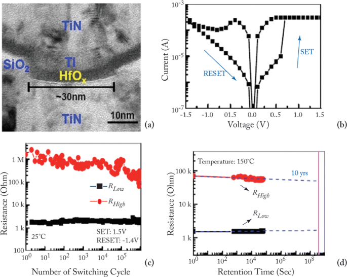
一 Transmission electron microscopy (TEM) image of TiN/Ti/HfO x /TiN RRAM device. b Typical current-voltage (I-V) characteristics of the device with 30-nm cell size. c 10 6 endurance switching cycles obtained from 500 μ s pulse. d A retention lifetime of 10 years is expected by testing at 150 ∘ C; reprinted from refs. [81, 103]
Uniformity
In RRAM cell, poor uniformity of various device characteristics is one of the significant factors limiting the manufacturing on a wider scale. The switching voltages, as well as both the HRS and the LRS resistances, are among the parameters exhibiting a high degree of variation. The variations of the resistance switching include temporal fluctuations (cycle-to-cycle) and spatial fluctuations (device-to-device). The stochastic nature of the formation and rupture of conductive filament is believed to be the main reason for these variations. Cycle-to-cycle and device-to-device variability is a major hindrance for information storage in RRAM devices [59]. The observation of cycle-to-cycle variability is influenced by the change in the number of oxygen vacancy defects that arise in the CF due to its stochastic nature of formation and rupture during the switching event [107]. Due to this random nature of the CF, the prediction and the precise control of the shape of the CF becomes extremely challenging. This variability becomes worse as the compliance limit (i.e. compliance current ‘I cc’) is reduced. On the other hand, for the higher value of ‘I cc’, the ratio of standard deviation (σ ) and average resistance (μ ) is low, resulting in a smaller LRS resistance spread. This is attributed to the higher defects in the CF, thus forming a well-defined path for current conduction.
RRAM also exhibits device-to-device (cell-to-cell) non-uniformity which also degrades the memory performance by reducing the memory margin between two states. The origin of this variability is attributed to the non-uniformities in the fabrication process such as the thickness of the switching film, etching damages and surface roughness of the electrodes. A lot of research has been conducted to improve the uniformity of RRAM and several methods have been explored for the same. One of the methods utilizes the concept of inserting nano-crystal seeds which confine the paths of the conductive filament by enhancing the effect of local electric field [82, 90, 108]. In Ti/TiO 2−x /Au-based RRAM [28], the induction of platinum (Pt) nano-crystals within the thin TiO 2−x results in an enhanced uniformity of the RRAM cell. The Pt nano-crystals limit the switching effect into regions with high oxygen vacancy generation probability which results in improved uniformity. In another approach, engineering the electrode/oxide interface by embedding appropriate buffer layers is very useful in achieving uniform RRAM operation. In HfO x -based RRAM [109], a thin Al buffer layer is inserted between the TiN electrode and HfO x oxide layer. This results in significant improvement of set voltage distribution as well as the resistance distribution, thus enhancing the uniformity of the device. The improvement in the SET voltage and the resistance distribution of the RRAM device after inserting a thin Al buffer layer between TiN electrode and HfO x bulk oxide and the same is depicted in Fig. 8 [59]. Al atoms are assumed to diffuse into HfO2 thin films, and they tend to localize oxygen vacancies due to the reduced oxygen vacancy formation energy, thus stabilizing the generation of conductive filaments, which helps to improve the resistance switching uniformity.
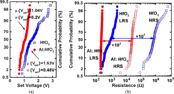
Uniformity improvement of Al buffered HfO x RRAM compared to HfO x -based RRAM array. 一 Statistical distribution of SET voltage (V set) obtained from 100 DC sweep cycles. b HRS and LRS statistical distribution for 100 pulse sweep cycles; reprinted from ref. [59]
In addition to the materials engineering approach, a novel programming method has also been suggested to reduce fluctuations. A multistep forming technique was implemented in W/HfO2/Zr/TiN [22]-based RRAM to minimize the overshoot current due to the parasitic effects. A multi-step forming technique results in the gradual formation of the filament; thus, a low set/reset current is achieved improving the switching characteristics of the device. Various other methods such as constant voltage forming and hot forming (usually referred to as forming at a higher temperature) have also been investigated to effectively reduce the resistance variations [110]. Another method of achieving high uniformity is by applying a pulse train rather than a single pulse to a RRAM cell [23]. This approach not only results in improved uniformity but also enhances the multilevel capability of a RRAM cell.
Effect of Operating Temperature and Random Telegraph Noise
To achieve a reliable performance of the RRAM device, the effect of operating temperature and random telegraph noise (RTN) is investigated. It is observed that the resistance of both the LRS and HRS states undergoes variations because of the change of operating temperature. The temperature study of TiN/HfO2/Ti/TiN [111] was carried out. A positive sweep voltage of <3 V magnitude and compliance current of 1 μ A was applied for the electroforming. Once forming takes place, a reset voltage (V reset) <–1 V switches the device back to the HRS (OFF state). To switch the device back to the LRS (ON state), set voltage (V set) <1 V is applied.
The reset operation in RRAM device tends to show voltage-controlled negative differential resistance (NDR). The reset operation occurs abruptly at low temperatures, while for temperatures above room temperature, the reset process takes place more gradually. The resistance of the RRAM device in the pristine state, as well as the ON state and OFF state as a function of temperature is depicted in Fig. 9a. The semiconducting behavior is observed for the pristine state as well as the OFF state, i.e. resistance decreases with increase of temperature. For the ON state, a metallic characteristic is observed, i.e. resistance increases with increase of temperature. Due to the variation of resistance with change in temperature, R OFF/R ON also decreases from a value of 20 to approximately 5 over the temperature range of 213–413K. In Ti/HfO x /Pt devices, decrease in R OFF/R ON was observed with temperature-dependent cycling. This decrease in resistance ratio was attributed to the built-up of oxygen-vacancy-related traps inside the HfO2 metal oxide layer [112, 113]. Additionally, temperature-dependent measurements without set/reset operation were carried out to evaluate the impact of I-V cycling on the R OFF/R ON ratio. The sweep voltage across the RRAM device was stopped before reaching V set and V reset values. For OFF state resistance (green rectangles), a weaker temperature dependence was observed in contrast to the ON state resistance (green circles) which exhibited similar characteristics, compared to the cycling case. From these observations, we infer that I-V cycling induces stronger temperature dependence, which decreases the R OFF/R ON ratio. The effect of temperature variation on the switching voltages V set and V reset is depicted in Fig. 9b. The slight variation in V set with changing temperature indicates that there is no significant temperature difference.对于 V 的情况 reset, the general trend is that a decrease in voltage value of about 0.2 V with temperature increase in the range of 233–333K is observed. Also, a slow increase of V reset is observed for 353–413K temperature range.
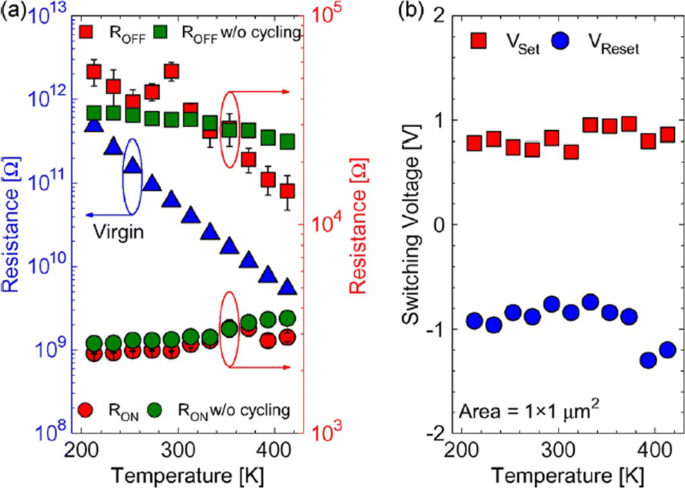
The effect of varying temperature on a virgin resistance (left axis) and the OFF-state as well as the ON-state resistances (right axis) at 213–413K temperature range and b switching voltages V set and V reset; reprinted from ref. [111]
Random telegraph noise (RTN) is another factor that affects the performance of RRAM. RTN has for long been used as an indicator of device performance and reliability. RTN decreases the memory margin between the HRS and LRS because of the extensive fluctuations in the read current during the read operation. Due to the effect of RTN, the read margin, scaling potential and the multilevel cell capability of a RRAM cell are greatly affected [114]; thus, it needs to be investigated to achieve reliable performance. To investigate the effect of bottom electrode on RTN, an analysis of Ta2O5/TiO2 RRAM [115] was carried out. The examples of complex RTN signals in LRS and HRS are depicted in Fig. 10. RTN causes read instability in the RRAM device, thus reducing the read margin, multibit storage implementation and hindering device scaling. The RTN is attributed to the trapping and de-trapping of electrons in the proximity of the CF in LRS whereas it occurs in the tunneling gap in the HRS state. Although the physics of RTN is still not clear and is being highly debated, the electron trapping and de-trapping which temporarily inhibits the charge transport is widely accepted as the mechanism responsible for fluctuation due to RTN. It is observed that with the decrease in operation current, the amplitude of RTN increases, thus highly affecting the HRS level. Therefore, it is necessary to ensure the additional resistance margin to achieve reliable performance. RTN in RRAM has been researched extensively, although the physical mechanism of RTN is still not explicitly defined. RTN can be utilized as a tool to map the movements of active vacancies in RRAM due to its time-dependent variation. This might be quite useful to understand the failure mechanisms of other reliability issues.
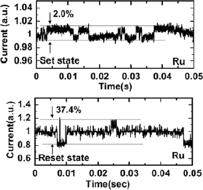
Complex RTN signals in LRS and HRS of Ta2O5/TiO2 -based RRAM depicting normalized noise amplitude and average current; reprinted from ref. [114]
Multilevel Resistive Random Access Memory (RRAM)
Multilevel Per Cell (mlc) Storage
Owing to their small physical size and low power consumption, RRAM devices are potential for future memory and logic applications. Increased storage density is among the most critical aspects of memory technology to enable the design of multibit capacity [89] memory cells. The multiple resistive states can be achieved in RRAM cells which provide benefits of low-cost and high-density non-volatile data storage solutions. Currently, a lot of research is being conducted in the area of RRAM to scale down the dimensions and increase the structural density of memory arrays. Previously, the storage density of RRAM has been increased by the reduction of device size; however, the complexity involved in the experimental procedures limits its successful implementation. Another suggested method is employing three-dimensional (3D) crossbar architectures. Two types of architectures of ‘vertical’ and ‘crossbar RRAM’ have been proposed [116, 117]; however, both these architecture types require advanced fabrication procedures which is not desirable. A much simpler alternative to increase storage density in RRAM devices is by making use of multilevel cell (MLC) storage technology which enables storing more than one bit per cell without reducing the physical device dimensions. This MLC is one of the most promising properties of RRAM which can significantly increase the memory storage density [83, 118–125]. Thus, instead of a single high and low resistance state (HRS and LRS), we can achieve multiple HRS and LRS, without changing the device dimensions. However, to achieve reliable MLC operation, the precise control over the resistance of the different resistance levels of RRAM should be ensured; otherwise, the device will suffer from resistance variability and reliability issues mainly due to the random nature of the conductive filament formation during the switching process [126].
Methods to Obtain Multilevel Per Cell (mlc) Modes in RRAM
The MLC behavior in RRAM makes it very useful for high-density applications. To obtain MLC behavior in RRAM, the following three methods are employed:(i) changing compliance current, (ii) controlling reset voltage and (iii) varying pulse width of program/erase operation.
MLC by Changing Compliance Current
The RRAM device is usually operated with 1-RRAM (1R) cell configuration [41] or in 1-Transistor 1-RRAM (1T-1R) cell configuration [18]. The MLC characteristics in 1R configuration can be obtained by changing the current compliance (I cc) during ‘set’ operation whereas the MLC characteristics in 1-Transistor 1-RRAM (1T-1R) cell structure are controlled by varying the voltage at the gate of the transistor, which enables the control of compliance current (I cc ) during the set operation of a RRAM cell. The typical MLC I-V curves of Ti/Ta2O5/Pt [127] based RRAM cell are shown in Fig. 11. As the compliance current (I cc) is increased from 150 μ A to 1 mA, six different LRS are obtained at I cc =150 μ A, I cc =200 μ A, I cc =300 μ A, I cc =500 μ A 和 I cc =700 μ A, I cc =1 mA due to the increase in the respective current of LRS (I LRS ) while the HRS is maintained constant and the HRS current (I HRS) remains same for all the LRS levels. For Ti/Ta2O5/Pt RRAM, with the increase in I cc, the maximum reset current (I reset) also increases while the set voltage is almost maintained constant. Also, it was observed that the resistance of the LRS (R LRS) decreases while the (I reset) increases owing to the stronger filament formation with the increase in I cc.
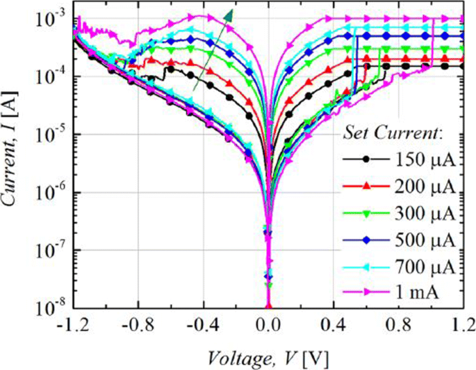
Multilevel characteristics of Ti/Ta2O5/Pt RRAM obtained by controlling the compliance current. ‘Reproduced from [127], with the permission of AIP Publishing’
The formation of the CF and its corresponding widening with an increase in I cc is the attributed mechanism of multilevel per cell (MLC) in compliance current (I cc) mode as depicted schematically in Fig. 12. With an increase in the size of CF because of an increase of I cc, the resistance of the CF decreases and hence results in multiple LRS levels for different values of I 抄送It is also observed that I reset increases with increasing I cc as higher power is required to rupture the CF having larger diameter.
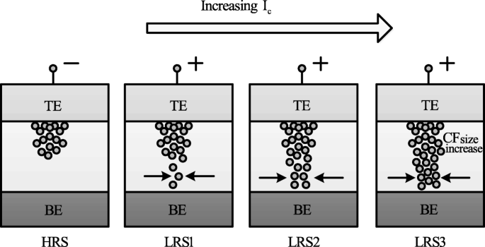
Schematic illustration of multiple resistance states in RRAM cell obtained by varying compliance current ‘I cc’ [98]
MLC by Controlling Reset Voltage
The MLC characteristics in a RRAM cell can also be obtained by controlling the reset voltage (V reset) while (I cc) is maintained constant. In this case, the typical MLC I-V curves of TiN/HfO x /AlO x /Pt-based RRAM cell [128] by applying different (V reset) of − 2.1 V, − 2.7 V and − 3.3 V are shown in Fig. 13.
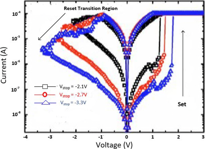
Multilevel characteristics of TiN/HfO x /AlO x /Pt RRAM obtained by controlling the reset voltage. ‘Reproduced from [128], with the permission of AIP Publishing’
It is observed that with an increase in (V reset), the HRS current (I HRS) decreases; thus, multiple HRS levels with the same LRS resistance are obtained. In addition, the set voltage (V set) also increases as V reset is increased while as the I reset remains almost constant.
The decrease in I HRS with the increase in reset voltage is primarily due to the increase in the gap between the metal electrode and tip of the CF as depicted in Fig. 14. The more the magnitude of the V reset, the larger the gap and thus the higher the value of resistance. Therefore, an increase in the gap between the CF tip and bottom electrode (BE) with increasing reset voltage results in multiple resistance levels of HRS. It is observed that the devices in which the I reset shows a gradual change in current instead of the abrupt change during the ‘reset’ operation, the change in HRS resistance in such devices can be due to decrease in the size of the conductive filament (CF) as V reset is increased. This approach is more viable practically for cross-point architectures as it requires relatively lower complex circuitry.
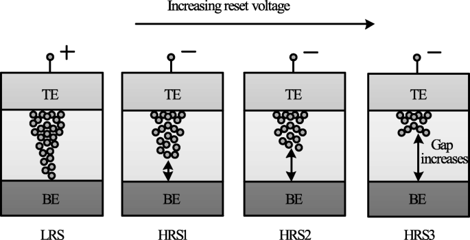
Schematic illustration of multiple resistance states in RRAM cell obtained by varying reset voltage ‘V reset’ [98]
MLC by Varying Program/erase Pulse Width
MLC characteristics can also be obtained by varying the program/erase pulse width while the amplitude of the pulse is maintained constant [23]. In HfO x -based RRAM [128], three HRS levels were demonstrated by varying the width of the reset pulse from 50 ns to 5 μ s。 This method of obtaining MLC characteristics in RRAM is relatively easier; however, this scheme is energy inefficient. This drawback limits the application of this method to obtain reliable characteristics in the RRAM cell. The higher energy consumption of the RRAM device was confirmed on the comparison of the transient responses between the reset pulse amplitude and pulse width control. This is particularly due to the higher unwanted energy dissipation as the thermal energy in the resistive switching material.
A summary of RRAM devices exhibiting multiple resistance states is shown in Table 4. As is evident from the table, various RRAM devices with multiple resistance states have been reported. Till date, however, only 8 resistance states have been demonstrated in a single RRAM cell either by varying I cc or V 重启。 Therefore, there is a huge scope for increasing the number of resistance states in the RRAM cell, thus enhancing its storage density.
<图>Modeling of RRAM Devices
Modeling plays a very critical role in development of devices utilizing semiconductor technologies. To fully understand device operation and to optimize the performance, an accurate model is of great importance. A number of RRAM models with varying features and accuracy have been proposed [129]. This section discusses the characteristics and attributes of the various commonly used RRAM models popular.
Stanford/ASU Model
One of the most popular physics-based RRAM models is the Stanford/ASU RRAM model [130–132], proposed by Guan et al. and Chen et al. This model was applied to validate the I-V switching characteristics of HfO2 RRAM [128] and includes the effect of Joule heating and temperature change on the switching of RRAM devices.
This model is dependent on the CF growth inside a dielectric switching layer. The filament gap, i.e. the gap between the tip of the CF and top electrode, is the internal state variable for this model. The growth of CF inside a dielectric is attributed to the oxygen ion movement and regeneration and recombination of oxygen vacancies [133]. Thus, the rate of change of filament gap (g) is given as [130]:
$$ {\frac{dg}{dt}} =V_{\tiny{0}}.\exp\bigg({{\frac{-E_{a},m}{k_{b}.T}} }\bigg). {\text{Sinh}} \bigg({\frac{qa_{h}\gamma V}{L.k_{b}.T}}\bigg) $$ (1)其中 E 一 is the activation energy, V is the magnitude of the voltage applied across the device, L is the switching material thickness, a h is the hopping distance, γ is the local field enhancement factor, V 0 is the velocity containing attempt to escape frequency, K b is the Boltzmann constant, q is the elementary unit charge and T is the temperature of the conductive filament.
The spatial variation in the gap size is accounted for in this model, in addition to the variations which arise due to the stochastic property of the ion process. A noise signal is added to the gap distance to account for these variations as [130]:
$$ g_{|t+\Delta t} =F \Big[ g_{|t}, {\frac{dg}{dt}} \Big] + \delta_{g}\times\tilde{X}(n)\Delta t, n ={\frac{t}{T_{GN}}} $$ (2)其中Δ t is the simulation time step, the function F represents time evolution of gap size fromt to Δ 吨。 \(\tilde {X}\)(n) is a zero mean Gaussian noise sequence. T GN is the time interval after which \(\tilde {X}\)(n ) changes to next random value.
The variation in the gap size δ g depends on kinetic energy of ions and filament temperature as [130]:
$$ \delta_{g} (T) ={\frac{\delta^{\tiny{0}}_{g}}{\bigg\{ 1+\exp \Big({\frac{T_{\text{crit}}- T}{T_{\text{smith}}}} \Big) \bigg\}}} $$ (3)where \(\delta ^{0}_{g}\) and T smith are fitting coefficients to match the resistance distribution curves to experiments and T crit is a threshold temperature above which the gap size changes significantly.
This model shows strong dependence on temperature; thus, there is a need to account for the change of ‘T’ . With change in cell characteristics, the dynamic inner domain temperature T changes significantly, while the outer domain assumed to be at uniform and stable temperature (T bath), is related as [130]:
$$ c_{p} {\frac{dT}{dt}} =V(t).I(t) - k(T-T_{\text{bath}}) $$ (4)where C p is the effective heat capacitance of inner domain, V (t) I (t) represents the Joule heating and k is the effective thermal conductivity.
Using a generalized conduction mechanism, the current conduction is defined as [130]:
$$ I(g,v) =I_{\tiny{0}}.\exp\bigg({{\frac{-g}{g_{\tiny{0}}}} }\bigg){\text{Sinh}} \bigg({\frac{V}{V_{\tiny{0}}}}\bigg) $$ (5)其中我 0, g 0 and V 0 are the fitting parameters to match experimental results.
One of the significant features of this model is its implementation in neuromorphic applications and RRAM synaptic device design [134], giving the model a great degree of flexibility and further scope for implementation in various neuromorphic systems.
Physical Electro-thermal Model
Physical electro-thermal model was developed by Kim et al. [135] and implemented with tantalum pentoxide (Ta2O5) -based bilayer RRAM [136–138]. This physical model solves the differential equations based on finite element solving method. This model also makes use of electrothermal physics phenomenon approach for modeling [139], thus giving it advantage in terms of flexibility to incorporate finite element method (FEM) solver to simulate the system very accurately. However, the drawback of this approach is its difficulty in implementation for SPICE and Verilog circuit solvers.
This model describes CF as a doped region having oxygen vacancies as dopants with CF extending from the top to the bottom electrode of the device. To describe the drift-diffusion of vacancy migration, this model assumes the same equation can be used to describe both the processes of oxygen ions and vacancies. The ion model by Mott and Gurney [140] is employed here to describe the process given as [135]:
$$ {\frac{dn_{D}}{dt}} =\Delta \times \bigg(D_{s}.\Delta_{n\tiny{D}}- \mu v n_{D} \bigg) + G $$ (6)其中 D s describes the diffusion process, v gives the drift velocity of vacancies and G is the CF growth rate which actually describes the SET process. The parameters are defined as [135]:
$$ D_{s} ={\frac{1}{2}} \times a^{2} \times f_{e} \times \exp \bigg({\frac{- E_{a}}{k_{B}T}} \bigg) $$ (7) $$ v =a_{h} \times f \times \exp \bigg({\frac{- E_{a}}{k_{B}T}} \bigg) \times {\text{Sinh}} \bigg({\frac{q a_{h}E}{k_{B}T}} \bigg) $$ (8) $$ G =A \times \exp \bigg({\frac{- (E_{a}-ql_{m}E)}{k_{B}T}} \bigg) $$ (9)where l m is the mesh size.
These equations govern the physical transformation of the device during SET and RESET transition, thus essentially controlling the CF growth and rupture.
Huang’s Physical Model
Huang’s physical model developed by Huang et al. [141, 142] is a very comprehensive physical model for RRAM device as it takes into account both the CF width and the gap of filament to electrode as the factors affecting the state variable dynamics. In addition, temperature distribution is also accounted for in this model.
SET/RESET process is considered as a result of generation/recombination process of oxygen ions (O 2− ) and oxygen vacancies (V 0)。 During the SET process, CF starts to evolve from the tip of the top electrode (T.E) and elongates in radius with increase in voltage, resulting in final width ‘W’ of the C.F. This model assumes symmetrical cylindrical shape of the C.F. During RESET process, CF ruptures starting from TE till it dissolves completely with increase in voltage. The filament gap distance ‘x’ is defined as the gap between active electrode layer (T.E) and the tip of the C.F.
Thus, for the SET process, parameter ‘W’ acts as state variable, while for RESET, parameter ‘x’ acts as state variable. Therefore, \(\frac {dx}{dt}\) and \(\frac {dw}{dt}\) define the dynamics of the device during the SET/RESET transition.
During the first reset process, CF reduction rate, i.e. release of O 2− , is by the electrode is expressed as [142]:
$$ {\frac{dx}{dt}} =a \times f\times \exp \bigg({\frac{- E_{i}-\gamma Z_{e}V}{k_{B}T}} \bigg) $$ (10)For O 2− hopping within the oxide layer, the CF reduction rate with ‘a’ being the distance between two V0 is given as [142]:
$$ {\frac{dx}{dt}} =a \times f\times \exp \bigg({\frac{- E_{h}}{k_{B}T}} \bigg) {\text{Sinh}} \bigg({\frac{ a_{h}Z_{e}E}{k_{B}T}} \bigg) $$ (11)For the case of RESET process when dominated by recombination between O 2− and V0 is expressed as [142]:
$$ {\frac{dx}{dt}} =a \times f\times \exp \bigg({\frac{- \Delta E_{r}}{k_{B}T}} \bigg) $$ (12)In the initial step of the SET process dominated by recombination of oxygen vacancies with thin CF initially grown is given by [142]:
$$ {\frac{dx}{dt}} =-a \times f_{e}\times \exp \bigg({\frac{- E_{a}-\alpha_{a} Z_{e}E}{k_{B}T}} \bigg) $$ (13)Here, Z 和 α g are the fitting parameters.
For the second step, CF grows along its radial direction and is defined as [142]:
$$ {\frac{dw}{dt}} =\bigg(\Delta w + {\frac{\Delta w^{2}}{2w}} \bigg) \times f_{e}\times \exp \bigg({\frac{- E_{a}-\gamma Z_{e}v}{k_{B}T}} \bigg) $$ (14)The current flowing through the device is modeled as a correlation of hopping current with voltage and gap distance expressed by [134] as:
$$ i =i_{0}. \exp \bigg({\frac{-x}{x_{T}}} \bigg) {\text{Sinh}} \bigg({\frac{v}{v_{T}}} \bigg) $$ (15)This model is validated in HfO x /TiO x system [141, 142], and a pretty accurate match between the experimental and simulation results is obtained. Although this model accounts for the significant processes which affect the RRAM operation, however, it has some limitations. The most critical one is being incompatible with the SPICE and Verilog-A.
Filament Dissolution Model
This model was developed exclusively for unipolar RRAM devices by Russo et al. [143–145], however was later modified for bipolar RRAM devices [139, 146] also. Filament dissolution model is based on rupture of CF under the effect of significant temperature change caused due to Joule heating.
One of the significant advantages of this model is that it utilizes the simple partial differential equations to account for the device current and temperature changes due to Joule heating as well as the dissolution velocity. The conduction of current within the device is described by Poisson’s equation [144] as:
$$ \triangledown \times \bigg({\frac{1}{\varphi}\triangledown_{v}} \bigg) =0 $$ (16)Here, φ is the oxide resistivity and v defines the electric potential due to the application of external bias voltage to one of the electrodes while the other electrode is connected to ground.
The CF is divided into a number of mesh grids and at each point of the mesh grid the temperature is calculated to describe the rupture of CF. The Fourier steady-state heat equation describes this effect as [144]:
$$ -\triangledown \times \bigg(k \triangledown T \bigg) =\varphi J^{2} $$ (17)其中 k represents the oxide layer thermal conductivity, J is the current density and T is the device temperature.
The temperature ‘T’ of the device increases to the critical temperature, after which the device is reset and the CF dissolution takes place. The dissolution factor is modeled as [144]:
$$ V_{\text{DIS}} =V_{\text{DIS}-F}. \exp \bigg({\frac{- E_{a}}{k_{B}T}} \bigg) $$ (18)其中 E 一 is the activation energy, k b is the Boltzmann constant, V DIS−F is a fitting parameter and V DIS is velocity of CF boundary towards symmetry axis.
The resistivity of CF is temperature-dependent and is described as [144]:
$$ \varphi_{\text{CF}} (T) =\varphi_{\mathrm{CF-RT}} \Big[ 1 + C (T-T_{0}) \Big] $$ (19)其中 C is the experimentally calculated temperature coefficient of resistivity and φ C F −R T is the standard CF resistivity at room temperature.
COMSOL Multiphysics Software [147] is used for solving the coupled equations for this RRAM model due to its multiphysics capabities and ability to handle such simulations.
Bocquet Bipolar Model
Bocquet bipolar model [148] describes the bipolar oxide-based resistive switching memories utilizing a physics-based modeling approach. Bocquet bipolar model describes the electroforming process of RRAM device, inaddition to utilizing some of the characteristics from Bocquet unipolar model [149] and modifies them significantly according to the bipolar switching characteristics. In this model, the radius of the CF is the internal state variable which effectively governs the switching rate.
To model the electroforming stage, Bocquet bipolar model utilizes electroforming rate (τ Form) which details the mechanism of conversion to switchable sub-oxide from pristine oxide. The electroforming stage is modeled as [148]:
$$ \tau_{\text{form}} =\tau_{\text{form}0} \times \exp \bigg({\frac{E_{a\text{Form}}-q \times \alpha_{s} \times V_{\text{cell}}}{k_{B}\times T}} \bigg) $$ (20) $$ {\frac{dr_{\text{CFmax}}}{dx}} ={\frac{r_{\text{work}}-r_{\text{CFmax}}}{\tau_{\text{form}}}} $$ (21)其中 E 一 Form is the activation energy for electroforming, τ form0 is the nominal forming rate, α s is the charge transfer coefficient, V cell is the voltage applied between the top and bottom electrodes, r CF is the radius of CF which varies from 0 to r CFmax, q is the elementary charge of electron, T is the temperature of the device and k B is the Boltzmann constant.
The electrochemical redox reaction derived from Butler-Volmer equation [150] is used to describe the SET/RESET operation as [148]:
$$ \tau_{\text{Red}} =\tau_{\text{Redox}} \times \exp \bigg({\frac{E_{a}-q \times \alpha_{s} \times V_{\text{cell}}}{k_{B} \times T}} \bigg) $$ (22) $$ \tau_{Ox} =\tau_{\text{Redox}} \times \exp \bigg({\frac{E_{a}+q \times (1 - \alpha_{s}) \times V_{\text{cell}}}{k_{B} \times T}} \bigg) $$ (23)Here, τ Red and τ Ox are the reduction and oxidation rates, respectively. τ Redox is the effective reaction rate considering both reduction and oxidation reactions.
The switching rate is obtained by coupling the above two equations as [148]:
$$ {\frac{dr_{CF}}{dt}} ={\frac{r_{\text{CFmax}}-r_{\text{CF}}}{\tau_{\text{red}}}} - {\frac{r_{\text{CF}}}{\tau_{\text{Ox}}}} $$ (24)Bocquet bipolar model is a quite comprehensive model as it includes the temperature effects as well. The local filament temperature is coupled using heat equation and is given in Eq.(25), the temperature considering a cylindrical-shaped filament is given in Eq. (26). The maximum temperature reached into CF at x =0, the middle of the filament is given in Eq. (27) and the equivalent electrical conductivity in the work area (σ eq ) is given in Eq. (28).
$$ \sigma_{x} \times F(x)^{2} =- k_{th}.{\frac{d^{2}T(x)}{dx^{2}}} $$ (25) $$ T(x) =T_{\text{amb}}+{\frac{V^{2}_{\text{cell}}}{2. L^{2}_{x}.k_{th}}} \bigg({\frac{L^{2}_{x}}{4}- x^{2}} \bigg) \sigma_{eq} $$ (26) $$ T =T_{\text{amb}}+{\frac{V^{2}_{\text{cell}}}{8. k_{th}}} \sigma_{eq} $$ (27) $$ \sigma_{eq} =\sigma_{CF}.{\frac{r^{2}_{\text{CF}}}{r^{2}_{\text{work}}}} - \sigma_{Ox}. {\frac{r^{2}_{\text{CFmax}}-r^{2}_{\text{CF}}}{r^{2}_{\text{work}}}} $$ (28)where (σ x ) is the local electrical conductivity, F (x ) is the local electric field, σ CF is the electrical conductivity of the conductive filament, k th is the thermal conductivity and T amb is the ambient temperature.
It must be mentioned here that temperature increases with increase in radius of the CF, resulting in self-accelerated reaction due to a positive feedback loop. The self-limited reaction also referred to as SOFT reset [151], on the other hand, occurs due to the decrease in temperature and radius of the CF during RESET operation.
The total current flowing in OxRRAM is the sum of currents flowing in the conductive area (I CF), the conduction through switchable sub-oxide (I sub−oxide) and conduction through unswitched pristine oxide (I pristine). The total current is as [148]:
$$ I_{\text{cell}} =I_{\mathrm{sub-oxide}} + I_{\text{CF}} + I_{\text{Pristine}} $$ (29) $$ I_{\text{CF}} =F.\pi. \sigma_{CF}.r^{2}_{CF} $$ (30) $$ I_{\mathrm{sub-oxide}} =F.\pi. \sigma_{Ox}. \big(r^{2}_{\text{CFmax}}- r^{2}_{CF}\big) $$ (31) $$ I_{\text{Pristine}} =S_{cell}.A.F^{2}. \exp {\frac{-B}{F}} $$ (32) $$ A ={\frac{m_{e}.q^{3} }{8\pi.h.m^{ox}_{e}.\phi_{b} }} $$ (33)The parameter B e is the metal-oxide barrier height (ϕ b )-dependent and is given as [148]:
$$ if \phi_{b}\geq qL_{x}F:B_{e} ={\frac{8 \pi \sqrt{2m^{ox}_{e} }}{3\times h\times q}} \Big[ \phi^{{\frac{3}{2}}}_{b}- (\phi_{b}-qL_{x}E)^{{\frac{3}{2}}} \Big] $$ $$ \text{otherwise}, B_{e} ={\frac{8 \pi \sqrt{2m^{ox}_{e} }}{3\times h\times q}} \times \phi^{{\frac{3}{2}}}_{b} $$ (34)where m e and \(m^{ox}_{e}\) are the effective electron masses into the cathode and oxide respectively, F =\(\frac {V_{\text {cell}} }{L_{x}}\) is the electric field across the active layer, h is the Planck constant and S cell is the section of the RRAM cell.
Discrete solutions are required to implement the model in an electrical simulator. This model accounts well in that aspect, making it suitable for simulation involving electrical circuits. This model implements equations in Eldo circuit simulator [152]. The discrete solutions are given as [148]:
$$ r_{\text{CFmax}_{i+1}} =\big(r_{\text{CFmax}_{i}}- r_{\text{work}} \big) \times e^{ {\frac{-\Delta t}{{\tau}_{\text{form}}}} } + r_{\text{work}} $$ (35) $$ r_{CF_{i+1}} =\bigg(r_{CF_{i}}- r_{\text{CFmax}_{i}} \times {\frac{\tau_{eq}}{\tau_{\text{Red}}}} \bigg) \times e^{ {\frac{-\Delta t}{{\tau}_{eq}}} } + r_{\text{CFmax}_{i}} \times {\frac{\tau_{eq}}{\tau_{\text{Red}}}} $$ (36) $$ \text{where} { \tau_{eq}} =\frac{\tau_{\text{Red}}\times \tau_{\text{Ox}} }{\tau_{\text{Red}}+\tau_{\text{Ox}}} $$ (37)This model has been verified against electrical characterization from an HfO2-based system [153]. An important feature of this model is that it can account effectively for device to device variability [154, 155]. One of the major limitations of this model is the lack of current or voltage threshold.
This section presents in detail various characteristics and features of the RRAM models. A comparative analysis of the RRAM models discussed in this work is presented in Table 5.
<图>Applications of RRAM
RRAM is seen as one of the standout candidates among the emerging memory technologies that has the potential for reforming the memory hierarchy primarily due to its high speed, the capability of non-volatile data storage, enhanced storage density and logic computing function. The various novel applications of RRAM are discussed in this section.
>Non-volatile Logic
The instruction codes and the data are transferred by making use of buses between various units in a computer system having von Neumann architecture because of the separate computing and memory unit. This data transferring process results increased energy consumption and time delay, which is commonly referred to as ‘von Neumann bottleneck’. For reducing the impact of von Neumann bottleneck [156], the computing process which utilizes RRAM crossbar array is suggested which alters the memory and computing operations in the same core. In addition, to obtain high integration density and low cost [157], two-terminal compact device structure of RRAM and its 4F 2 array architecture are highly beneficial. For example, to obtain simple Boolean logic functions such as ‘logic NOT’, ‘logic AND’, and ‘logic OR’, we require multiple transistors and each single transistor takes 8−10F 2 区域。 These logic functions can be realized by making use of two or three RRAM cells, resulting in total approximate area of around 10F 2 only [158].
Till date, several methods have been suggested for realizing Boolean logic functions [159, 160]. Boolean computing is significantly more established compared to existing non-Boolean computing paradigms such as neuromorphic computing and quantum computing. Therefore, energy and cost-efficiency of CPU or MCU can be enhanced without the need to develop new algorithms or software, although there is still a lack of technical solution on how to implement complex computing tasks in a crossbar array. Thus, most of research to date focusses on only basic logic level demonstration as it becomes quite complex to implement a whole computing unit using RRAM array.
Neuromorphic Computing
To overcome ‘von Neumann bottleneck’, one of the effective ways is brain-inspired neuromorphic computing which has shown promising potential in a wide range of complex and cognitive tasks like visual/audio recognition, self-driving, and real-time big-data analytics. Compared to CMOS-based neuromorphic network, neuromorphic computing based on RRAM-array offers advantages in terms of on-chip weight storage, online training, and scaling up to much larger array size [161–163]. In addition, the processing speed of RRAM improves by three orders of magnitude, whereas the power consumption rate is reduced by four orders of magnitude [164].
For realizing hardware-implemented neuromorphic computing paradigms, two methods are suggested:one among the strategies mimics the structure and working mechanism of biological neural networks while the other method works on accelerating the existing artificial neural network (ANN) algorithms. In a neural network, a synapse is used to transfer spikes between different neurons in addition to storing information about the transferring weights. The information regarding weights can be acquired through certain learning rules such as spike-time-dependent plasticity (STDP) and spike-rate-dependent plasticity (SRDP) [165–167]. Although some of the works reported in the literature have tried to emulate such learning rules on RRAM devices, it is however quite complicated to extend such types of bioinspired learning rules to a complex task as the theoretical algorithm is still lacking.
A practically viable approach is to map an ANN to a RRAM-based neuromorphic network directly. Some advanced tasks such as pattern and speech recognition have been demonstrated based on this method [166–169]. Although very promising, RRAM-based synapse is still far from being applied as various issues such as material optimization, variation suppressing, control circuit design, architecture, and algorithms design for analog computing need to be addressed effectively.
Security Application
The security aspect has become more prominent with rapid developments in the field of information technology; thus, there is a need for hardware-based security-integrated circuits. In contrast to security circuits based on CMOS logic which exploits the random nature of the semiconductor manufacturing process, security circuits based on RRAM are more robust to attacks of various types due to its completely random switching mechanisms [170, 171]. It must be noted that for security applications, larger variation of RRAM device parameters such as random telegraph noise (RTN), resistance variations and probabilistic switching is desirable, which is quite different from memory applications that require a smaller degree of variation among numerous parameters.
A novel security feature commonly referred to as physical unclonable function (PUF) [172], based on RRAM is proposed for device authentication (strong PUF) and key generation (weak PUF) applications. Significantly larger number of input-output pairs [also called challenge-response pair (CRP) are required for strong PUF, while only a small amount of CRPs of extremely higher reliability are required for weak PUF [173]. Although, PUFs based on RRAM have demonstrated remarkable performance; however, still more practical demonstrations and further evaluations are required to work out the maturity of this new primitive within the field of hardware security.
Non-volatile SRAM
Volatile memory technologies like SRAM and DRAM may consume over half of the static power within the current mobile SoC chips. Thus, to attain fast parallel memory operations, reduced area and low-energy consumption, RRAM-based non-volatile SRAM (nvSRAM) was proposed [174] in which two RRAM cells are stacked on eight transistors, forming an 8T2R structure. Also, non-volatile ternary content-addressable memory (TCAM) having 4T2R cell structure [175] and non-volatile flip flops having reduced stress time and write power based on RRAM have been demonstrated recently [176].
Challenges and Future Outlook
During the past several years, research in the field of emerging memory technologies has grown significantly and several prototype RRAM products have been developed demonstrating the potential for high-speed and low-power embedded memory applications. RRAM is one of the most promising memory technologies because of the advantages of simple structure, compatibility with the existing CMOS technology, good switching speed and ability to scale to the smallest dimensions. As a matter of fact, currently the Flash memory technology is facing difficulties to reduce to lower dimensions and as such RRAM is emerging as a potential replacement especially for fast operation and medium size storage density memory applications.
One of the most critical aspects that needs to be thoroughly investigated is that of the reliability of RRAM. A mechanism must be developed to ensure the detection of the operation failure of the device. Also designing circuits, e.g. a test element group (TEG) design for robust signal sensing, is one of the critical challenges for the emergence of RRAM devices. To achieve high-density memory operation in RRAM, the 1D1R operation is essential. This can be realized by operating the RRAM device in the unipolar mode. However, in the unipolar operation, higher current is needed for the reset process as compared to that of the bipolar operation. This is due to the fact that thermal effect plays a significant role in the unipolar reset process. Thus, to realize a high-density 1D1R RRAM array, the thermal effects both inside and outside a memory element needs to be considered. Also note that till date, in a single RRAM device, no technology has simultaneously reported fast switching, low power, and stable operation. Although, the endurance of RRAM has been reported as high as 10 12 [59], it is still not enough to be able to replace DRAM. The RRAM possesses the switching speed fast enough for DRAM replacement and the materials used in the fabrication for RRAM are very similar to that of DRAM, it becomes a critical challenge to improve the endurance characteristics of RRAM. To improve the endurance characteristics, it is necessary to control the oxygen movement between the electrode and the oxide layer at the interface. It is suggested to insert the second metal layer at the interface which can be easily oxidized and acts as an oxygen reservoir to prevent oxygen from penetrating into the electrode during the resistance switching. The most critical challenge hindering RRAM development till date is the proper understanding of the device switching mechanism which is since long being debated by researchers across the globe. The inconsistent switching mechanism of various reported RRAM devices is believed to be because of variation in the fabrication process, and thus, more rigorous analysis is needed in the future for obtaining a better understanding of the switching mechanism of RRAM devices. The aforesaid issues need to be handled effectively before implementing RRAM in future memory applications. Although, RRAM is highly attractive for use in neuromorphic computations, the biggest challenge to industrialize RRAM lies in its ability to tackle the variability issues, not only at nominal operating conditions but also at high temperatures before they can be used in a wide variety of applications.
Conclusion
This review article provides a brief introduction into the advancement of the memory architecture, the current trends and the limitations while providing a valuable insight into the field of emerging memory technologies. A detailed discussion, highlighting the importance of RRAM, its structure, working mechanism, and classification, has been presented. The key performance parameters and their effect on the RRAM operation has also been detailed within the current manuscript. An elaborate study on the MLC capability of RRAM, along with the methodology have been presented. The manuscript also discusses the important features of the widely accepted RRAM models. The implementation of RRAM for various important applications such as non-volatile logic, neuromorphic computing, security, and non-volatile SRAM have been highlighted. Although, significant success has been achieved in RRAM technology; however, more work is needed as RRAM still suffers from various challenges in terms in terms of high operation current, lower resistance ratios, and reliability issues. More efforts in research should aim to develop methods to achieve faster programming/erasing, lower power consumption, enhancing the storage density by implementing multilevel storage capability and improvement in the fabrication process for enhanced uniformity. In addition, renewed focus should be towards use of RRAM in embedded memory and non-volatile logic applications as breakthroughs in these fields are much more exciting and significant. With continued work and improvements, it is imperative that RRAM devices will be a standout technology for future non-volatile memory applications.
数据和材料的可用性
不适用。
缩写
- RRAM:
-
Resistive random access memory
- MLC:
-
Multilevel cell
- RTN:
-
随机电报噪声
- DRAM:
-
动态随机存取存储器
- SRAM:
-
Static random access memory
- PCM:
-
Phase change memory
- STT-MRAM:
-
Spin-transfer torque resistive random access memory
- LRS:
-
低阻态
- HRS:
-
高阻态
- MTJ:
-
Magnetic tunneling junction
- MIM:
-
金属-绝缘体-金属
- MoM:
-
Metal-oxide-metal
- PLD:
-
Pulse laser deposition
- ALD:
-
原子层沉积
- V set :
-
Set voltage
- V reset :
-
Reset voltage
- V f :
-
Forming voltage
- I CC :
-
Compliance current
- CBRRAM:
-
Conductive bridge resistive random access memory
- OxRRAM:
-
Oxygen vacancies resistive random access memory
- ECM:
-
Electrochemical metallization memory
- VCM:
-
Valence change memory
- CF:
-
Conductive filament
- 基础:
-
底部电极
- TEM:
-
透射电子显微镜
- I-V:
-
电流-电压
- 1T-1R:
-
1-Transistor 1-RRAM
- ANN:
-
人工神经网络
- STDP:
-
Spike-time-dependent plasticity
- SRDP:
-
Spike-rate-dependent plasticity
- PUF:
-
Physical unclonable function
- CRP:
-
Challenge-response-pair
- nvSRAM:
-
Non-volatile SRAM
- TCAM:
-
Ternary content addressable memory
- TEG:
-
Test element group
纳米材料
- 13种耐火材料及其应用
- 提高物联网可穿戴设备的性能和安全性
- Cervoz:为工业应用选择合适的闪存
- HfO2/TiO2/HfO2 三层结构 RRAM 器件在原子层沉积制备的 Pt 和 TiN 涂层衬底上的双极电阻开关特性
- 无合规性 ZrO2/ZrO2 − x /ZrO2 具有可控界面多态切换行为的电阻式存储器
- 通过纯 CMOS 逻辑工艺具有自抑制电阻开关负载的 RRAM 集成 4T SRAM
- 氮化处理的基于 HfO2 的 RRAM 中的传导机制和改进的耐久性
- 电阻式随机存取存储器建模和仿真的集体研究
- 具有超快速和稳定电荷存储性能的分层大孔石墨纳米网
- 聚苯胺/氮掺杂有序介孔碳复合材料的合成和超级电容器性能
- 通过随机空位模型研究接触电阻随机存取存储器的可变性
- V/SiOx/AlOy/p++Si 器件作为选择器和存储器的双重功能


