

4H-SiC 分离吸收电荷和倍增雪崩光电二极管结构的优化策略以提高紫外线检测效率
摘要
在这项工作中,系统地对基于 4H-SiC 的分离吸收电荷和倍增 (SACM) 雪崩紫外光电二极管 (UV APD) 进行了结构优化的参数研究。根据我们的结果,击穿电压会受到倍增层的厚度和电荷控制层的掺杂浓度的强烈影响。 n型欧姆接触层、吸收层和电荷控制层的厚度可以显着影响光穿透深度,相应地影响光生电子-空穴对的数量,因此上述层厚度具有对 SACM APD 的响应度有很大影响。为了提高 APD 的响应度,我们需要降低光吸收层和电荷控制层界面处的能带势垒高度,以便促进载流子传输到倍增层。此外,我们研究了具有较小角度的正斜面台面,以减少台面边缘的电场。从而相应地抑制了暗电流。
介绍
作为宽带隙半导体材料,碳化硅(SiC)和氮化铝镓(AlGaN)表现出优异的材料特性,如临界电场高、抗辐射效果更好、导热性好,使其适用于紫外线(UV)检测 [1,2,3]。基于 AlGaN 的光电探测器在 3.4 和 6.2 eV 之间的可调带隙使可控截止响应波长范围从 365 到 200 nm。然而,由于难以生长高质量的富含 Al 的 AlGaN 化合物,AlGaN 基光电探测器的暗电流高于 SiC 基对应物的暗电流 [4]。因此,基于 SiC 的光电探测器引起了广泛的研究兴趣。迄今为止,基于 4H-SiC 的固态紫外探测器包括肖特基势垒二极管、金属-半导体-金属 (MSM) 光电二极管、p-i-n 光电二极管和雪崩光电二极管 (APD) [5,6,7,8,9]。由于雪崩增益高、暗电流小、噪声低等优点,4H-SiC紫外APD在火警、量子通信、导弹探测等许多需要弱紫外信号检测的前沿领域具有广阔的应用前景。 10,11,12]。然而,SiC材料的光吸收系数较低,因此普通的倍增层较薄的光电二极管结构难以实现高量子效率。直到提出分离的吸收电荷和倍增 (SACM) 结构 APD,问题才得到解决。一方面,紫外光可以被吸收层有效吸收,另一方面,高场倍增层可以通过碰撞电离过程获得高内增益。电荷控制层可以终止倍增层中的碰撞电离过程 [13, 14]。 SACM 结构的优势在于噪声降低,因为只有具有较大电离率的单一类型的光生载流子才能注入倍增层 [15, 16]。为了获得对弱紫外信号的高探测率,应制造具有大活动探测面积的 SACM APD [17]。然而,增加的器件尺寸伴随着显着增强的表面漏电流和体漏电流。因此,这不仅对 SiC 外延片的质量提出了严格的要求,也反映了对器件制造工艺和器件设计的巨大挑战。在过去的几十年里,Cree 公司大力推广了 SiC 薄膜的外延生长技术,从而进一步推动了晶体质量的不断提高。最近,周等人。提出了一种可变温度光刻胶回流技术,为斜切的 4H-SiC APD 台面创造非常光滑的侧壁 [18],从而实现超过 10 6 的高倍增增益 以及 ~ 0.2 nA/cm 2 的低暗电流 .尽管如此,之前的研究更侧重于提高材料质量和优化 SACM APD 的制造技术 [19,20,21],而结构设计对光生载流子传输和光电流检测率的影响至今鲜有讨论.因此,在这封信中,我们系统地研究了具有不同结构设计的大面积 4H-SiC 基 SACM 紫外 APD 的光电性能。同时,还提供了有见地的实物图片和讨论。我们相信这项工作的发现有助于研究人员以更低的成本优化 4H-SiC APD。
众所周知,当碰撞电离发生时会产生大规模的载流子倍增,然而,这受到倍增层的厚度和电荷控制层的掺杂浓度的强烈影响。在倍增层中产生非常强的电场,以实现碰撞电离。由于其中较大的掺杂浓度,电荷控制层可以终止电场。此外,我们还发现,通过调制吸收层和电荷控制层之间的能带,我们能够调整光谱响应率。合理采用正斜面台面可以显着降低侧壁表面电场,有助于抑制暗电流和边缘击穿。后续会进行详细的分析和讨论。
研究方法和物理模型
图 1a 显示了本工作中采用的标准 4H-SiC SACM APD 的横截面示意图,其具有 n + 型 4H-SiC 层作为衬底。然后,架构堆栈包括一个 3 微米厚的 p + - 类型层 (N 一 =1 × 10 19 厘米 −3 ) 作为 p 型欧姆接触层,0.5 微米厚的 n − -type 乘法层 (N d =1 × 10 15 厘米 −3 ) 用于载流子倍增,0.2 微米厚的 n 型电荷控制层 (N d =5 × 10 18 厘米 −3 ) 用于终止碰撞电离过程,以及一个 0.5 微米厚的 n − -型吸收层(N d =1 × 10 15 厘米 −3 ) 来吸收入射光子。在器件结构的顶部,有一个 0.3 微米厚的 n + - 型欧姆接触层 (N d =1 × 10 19 厘米 −3 )。正斜角 (θ =8°) 是为台面结构创建的,以抑制边缘击穿 [22, 23]。 4H-SiC SACM APD 的直径为 800 μm。在我们的计算中,阴极和阳极接触都被认为是理想的欧姆接触。根据图 1c 和 d,我们的结果表明,上述标准 4H-SiC SACM APD 结构的计算结果显示出 2.5 nA/cm 2 的暗电流 ,击穿电压为 161.6 V,在 280 nm 波长处的峰值响应率为 0.11 A/W。计算出的标准 4H-SiC SACM APD 的电流-电压特性和响应度与实验数据一致。这充分证明了本文使用的碰撞电离、4H-SiC材料吸收系数、泊松方程、电流连续性方程和漂移扩散方程是合理的。在这里,我们以图 1a 中的结构作为研究基准,而研究的变量包括斜台面角度、厚度和每层的掺杂浓度。
<图片>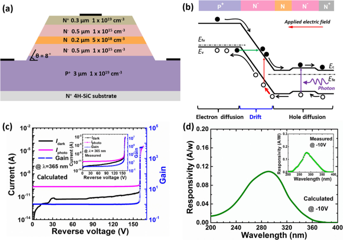
一 横截面结构示意图(未按比例绘制),b 标准4H-SiC SACM APD在反向偏压下的能带示意图,c 计算的电流-电压特性和倍增增益,以及 d 计算标准 4H-SiC SACM APD 在 10 V 反向电压下的光谱响应特性。 c 中的插图 显示了测得的电流-电压特性和倍增增益。 d 中的插图 显示了测量的标准 4H-SiC SACM APD 的光谱响应特性,偏置在 - 10 V
为了更好地理解不同结构变量对 4H-SiC SACM APD 光电性能的影响,图 1b 显示了反向偏置下的能带示意图。吸收层中的光生电子-空穴对将通过电荷控制层扩散到倍增层中。光生电子-空穴对到达倍增区后,会被耗尽的电场分开。孔随后将在倍增层中经历倍增过程,从而产生内部电流增益。同时,光生电子将返回阴极并在不经历碰撞电离的情况下转化为电流。影响光电流的重要因素包括倍增层中的电场分布、电荷控制层中的能带排列、吸收层和 n 型欧姆接触层,其中任何能垒都会阻碍载流子传输。还值得注意的是,倍增层中的电场分布可由倍增层和电荷控制层的掺杂浓度决定。同时,斜台面角度也基本上与电场分布相关。我们还要注意每一层的厚度,以确保高效的载流子扩散过程。因此,系统地研究这些关键结构参数对于优化器件性能具有重要意义。
数值研究由APSYS进行,它可以在适当的边界条件下求解电流连续性方程、泊松方程和漂移扩散方程。碰撞电离和齐纳隧穿过程都包含在漂移扩散方程中。载流子传输过程的载流子-载流子散射也包含在低场迁移率模型中。 Shockley-Read-Hall (SRH) 复合寿命假定为 1 μs [24]。具体来说,字段 (E ) 电子碰撞电离系数的相关性 (α n ) 和孔 (β p ) 对于 4H-SiC 基层可以分别用 Chynoweth 公式 (1) 和 (2) 表示如下 [25]:
$$ {\alpha}_n=1.98\times {10}^6\exp \left[-{\left(\frac{9.46\times {10}^6}{E}\right)}^{1.42}\ right]{\mathrm{cm}}^{-1} $$ (1) $$ {\beta}_p=4.38\times {10}^6\exp \left[-{\left(\frac{1.14\次 {10}^7}{E}\right)}^{1.06}\right]{\mathrm{cm}}^{-1} $$ (2)4H-SiC 材料在不同波长 (λ) 方面的吸收系数 (∂) 由下式计算。 (3) [26]:
$$ \partial =-790.3+18.2\uplambda -0.17{\uplambda}^2+8.57\times {10}^{-4}{\uplambda}^3-2.39\times {10}^{-6}{ \uplambda}^4+3.53\times {10}^{-9}{\uplambda}^5-2.16\times {10}^{-12}{\uplambda}^6 $$ (3)数值模型中使用的其他材料参数可以在别处找到 [27]。计算基于有限元方法,需要用户适当调整网格分布才能进行准确计算。
结果和讨论
n 型欧姆接触层的结构参数对光电性能的影响
为了探究n型欧姆接触层的厚度和掺杂浓度对光电性能的影响,我们分别设计了参考器件,器件L1至L4和器件A1至A4。请注意,参考设备是基本的 SACM APD 结构,如图 1a 所示。除了 n 型 SiC 欧姆接触层外,其他提议的 APD 与参考器件相同,其详细结构信息如表 1 所示。
我们首先根据图 2a 中的 n 型 SiC 欧姆接触层(即器件 L1 到 L4)的厚度显示击穿电压。图 2a 的插图选择性地展示了暗电流、365 nm 光照下的光电流以及器件 L1 的增益。对于器件L1,击穿电压为~ 161.6 V,暗电流密度保持在~ 2.5 nA/cm 2 当偏置低于 161.6 V. 注意击穿电压是在电流为 10 -5 A. 发生碰撞电离过程时暗电流增加。当365nm光照照射到器件上时,线性区域的光电流水平变高,这表明倍增增益可以超过10 3 对于器件 L1 的反向电压为 161.6 V。五个研究的 APD 的雪崩击穿电压总结在图 2a 中。从图 2a 可以看出,n 型欧姆接触层的厚度对击穿电压的影响可以忽略不计。为了揭示观察的潜在机制,我们计算并显示了图 2b 中参考器件和器件 L1 到 L4 的垂直电场分布,这说明电荷控制层限制了耗尽区和电场的边界。乘法层。因此,我们可以推测 n 型欧姆接触层不会影响倍增层中的电场分布,这在图 2b 中得到了证明。图 2b 中的观察结果很好地解释了图 2a 中参考器件和器件 L1 至 L4 的相同击穿电压。接下来,我们展示了图 2c 中五个器件的光生电流。为了获得更好的分辨率,我们收集了偏置为 100 V 的光生电流,如图 2c 的插图所示。我们可以看到,随着 n 型欧姆接触层厚度的增加,光生电流减小。过厚的n型欧姆接触层会导致光生载流子发生非辐射复合,相应地降低扩散电流。利用光生电流,我们可以得到参考器件和器件 L1 至 L4 在图 2d 中反向电压为 100 V 时的光谱响应度。五个研究设备的峰值响应波长集中在 280 nm。响应度随着 n 型接触层厚度的增加而降低,这与图 2c 的插图一致。因此,我们在此总结,n型4H-SiC欧姆接触层的厚度应适当减薄,以避免非辐射复合增加和扩散电流降低。
<图片>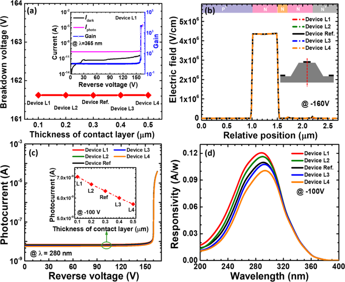
一 击穿电压,b SACM APD 的垂直电场分布偏置在 − 160 V, c 280 nm光照下的光电流-电压特性,以及d SACM APD 的光谱响应特性分别偏置在 - 100 V 的参考器件和具有不同厚度的 n 型欧姆接触层的器件 L1 到 L4。 a 中的插图 显示了计算出的电流-电压特性和器件 L1 的倍增增益。 c 中的插图 显示了参考器件和器件 L1 到 L4 的光电流偏置在 - 100 V
接下来,我们通过分析图 3a 中的参考器件和器件 A1 至 A4,研究击穿电压与 n 型欧姆接触层中的掺杂浓度的函数关系。图 3a 中的插图显示了暗电流、光生电流和器件 A1 施加的偏压方面的增益。击穿电压定义为电流达到 10 -5 A. 根据图 3a,击穿电压几乎不取决于 n 型 4H-SiC 欧姆接触层中的掺杂浓度。如前所述,电荷控制层可以有效地限制倍增层中的耗尽区和电场。因此,n 型欧姆接触层中掺杂浓度的变化不会影响器件内部的电场分布 [见图 3b]。然后,我们根据图 3c 中参考器件和器件 A1 至 A4 的施加偏压计算并显示光生电流。从图 3c 可以看出,n 型欧姆接触层的掺杂浓度对光电流偏置的影响可以忽略不计。五种研究设备在不同波长下的光谱响应率如图 3d 所示。数据是在 100 V 的反向电压下计算的。最大响应度为 ~ 0.11 A/W 的波长为 280 nm。与图 3c 一致,响应度不太依赖于 n 型欧姆接触层中的掺杂浓度。因此,我们得出结论,与 4H-SiC SACM APD 的 n 型欧姆接触层的掺杂浓度相比,响应度受厚度的影响更大。我们还建议增加载流子扩散长度以提高响应度。
<图片>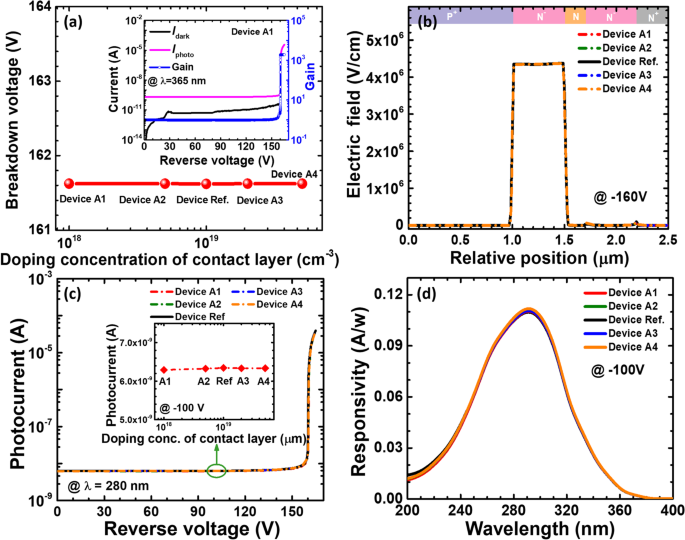
一 击穿电压,b SACM APD 的垂直电场分布偏置在 − 160 V, c 280 nm光照下的光电流-电压特性,以及d SACM APD 的光谱响应特性,分别针对参考器件和具有不同 n 型欧姆接触层掺杂浓度的器件 A1 至 A4 偏置在 - 100 V。 a 中的插图 显示了计算出的电流-电压特性和器件 A1 的倍增增益。 c 中的插图 显示参考器件和器件 A1 到 A4 的光电流偏置在 - 100 V
吸收层结构参数对光电性能的影响
在本节中,研究了吸收层的厚度和掺杂浓度对 4H-SiC 基 SACM APD 光电性能的影响。 SACM APD 吸收层的详细结构信息汇总并显示在表 2 中。除了吸收层之外,器件 M1 至 M4 和器件 B1 至 B4 在结构上与参考器件相同。器件M1至M4具有不同的厚度,而器件B1至B4的吸收层掺杂浓度不同。
通过使用参考器件和器件 M1 到 M4,图 4a 显示了吸收层不同厚度的击穿电压。出于演示的目的,我们计算并呈现了暗电流、光生电流和增益作为图 4a 插图中器件 M1 施加的偏置的函数。电流为10 -5 时采集击穿电压 A. 我们可以看到击穿电压几乎不取决于吸收层的厚度。众所周知,击穿电压强烈受轻掺杂倍增层中电场强度的影响,因此,图 4b 显示了五个研究器件在 - 160 V 的反向偏压下的垂直电场分布。参考设备和设备 M1 到 M4 的场分布完全相同,这证实了图 4a 中的结论。我们随后在图 3 和图 5 中展示了光生电流和响应度。分别为 4c 和 d。光生电流 [参见图 4c 的插图] 和响应率都显示出随着吸收层厚度的增加而降低的趋势。为了进一步解决潜在机制,我们还计算并显示了图 4e 中倍增层内的载流子分布,当反向偏压为 100 V 时,五个研究的器件。我们可以看到电子和空穴浓度水平随着吸收层厚度的增加而降低,这归因于当吸收层变厚时增强的非辐射复合。非辐射复合消耗载流子,从而抑制扩散电流和响应度。在此,为了避免非辐射复合引起的载流子消耗,我们建议吸收层不能太厚以获得高探测率的4H-SiC SACM APD。
<图片>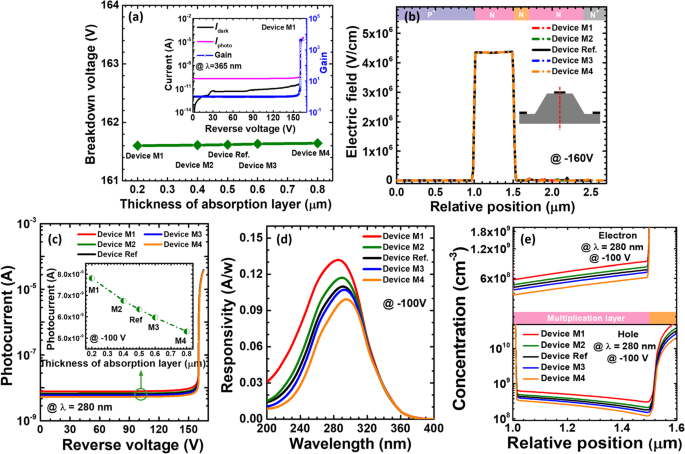
一 击穿电压,b SACM APD 的垂直电场分布偏置在 − 160 V, c 280 nm光照下的光电流-电压特性,d 光谱响应特性,以及e SACM APD 倍增层中的载流子浓度分布,分别为参考器件和具有不同吸收层厚度的器件 M1 至 M4 偏置在 - 100 V。 a 中的插图 显示了计算出的电流-电压特性和器件 M1 的倍增增益。 c 中的插图 显示参考器件和器件 M1 到 M4 的光电流偏置在 - 100 V
除了吸收层厚度外,吸收层的掺杂浓度对器件性能也有显着影响。然后我们计算并显示图 5a 中参考器件和器件 B1 到 B4 的击穿电压。击穿电压定义为电流为 10 -5 A 如图 5a 的插图所示。从图 5a 可以看出,吸收层的掺杂浓度对击穿电压没有显着影响。可以通过图 5b 中的垂直一维电场分布进一步证明,吸收层的掺杂浓度不会显着改变倍增层中的电场分布。我们还展示了图 5c 中所研究器件在 280 nm 波长处的光生电流,这表明当吸收层中的掺杂浓度增加时,光生电流得到改善。与图 5c 一致,图 5d 中的波长相关响应率也随着吸收层的掺杂浓度增加而受到青睐,例如器件 B4。
<图片>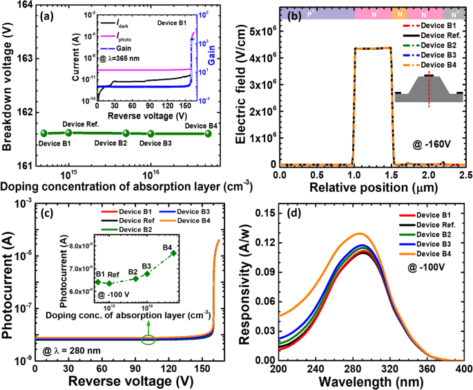
一 击穿电压,b SACM APD 的垂直电场分布偏置在 − 160 V, c 280 nm光照下的光电流-电压特性,以及d SACM APD 的光谱响应特性分别偏置在 - 100 V 的参考器件和具有不同吸收层掺杂浓度的器件 B1 至 B4。 a 中的插图 显示了计算出的电流-电压特性和器件 B1 的倍增增益。 c 中的插图 显示了参考器件和器件 B1 到 B4 的光电流偏置在 - 100 V
为了显示器件 B4 增强响应的深度起源,我们显示了图 1 和图 2 中器件 B1 和 B4 的电荷控制层、吸收层和 n 型欧姆接触层的能带分布。分别为 6a 和 b。这里值得一提的是,电荷控制层和n型欧姆接触层的掺杂浓度为5 × 10 18 厘米 −3 和 1 × 10 19 厘米 −3 , 分别。因此,吸收层的较低掺杂浓度可以产生内置电场并在电荷控制层/吸收层/n 型欧姆接触层的界面处产生能量势垒[28]。能量势垒可以阻止光生载流子扩散到倍增层中。一种可以降低势垒的非常方便的方法是增加吸收层中的掺杂浓度。结果,有效价带势垒值ψ v 对于器件 B1 和 B4,电荷控制层的电压分别为 513 meV 和 480 meV。可以看到,吸收层掺杂浓度的增加促进了光生空穴的传输 [见图 6c]。一旦更多的光生空穴可以注入倍增区,碰撞电离就会变强,从而导致光生电流和响应度增加。
<图片>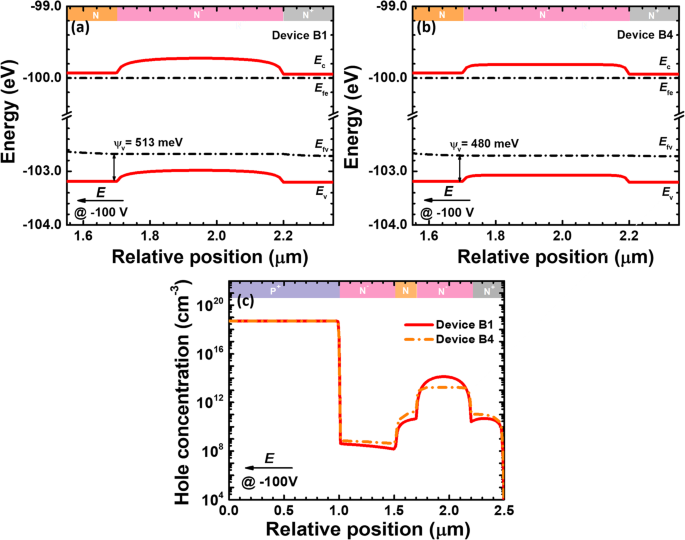
a的电荷控制层、吸收层和n型欧姆接触层的能带图 设备 B1 和 b 设备 B4,c 器件 B1 和 B4 在 280 nm 光照下的空穴浓度分布。数据是在100 V的反向电压下计算的
电荷控制层结构参数对光电性能的影响
为了探究电荷控制层的厚度和掺杂浓度对光电性能的影响,我们为电荷控制层设置了不同的架构信息,如表 3 所示。器件 N1 至 N4 和器件 C1 至 C4 仅与参考器件不同在电荷控制层。 N1~N4和C1~C4器件采用不同的掺杂浓度和层厚。
如前所述,实现碰撞电离和雪崩击穿的电场主要限制在倍增层中。作为图 7a 中电荷控制层厚度函数的击穿电压推断电荷控制层的厚度对载流子倍增过程的影响非常小。通过显示图7b进一步证明了这一点。图 7c 展示了在参考器件和器件 N1 至 N4 的施加偏压方面的光生电流。一旦电荷控制层厚度增加,光生电流变低,这也随着电荷控制层厚度的增加而转化为更小的响应度。我们还归因于消耗载流子并抑制扩散电流的增强的非辐射复合。
<图片>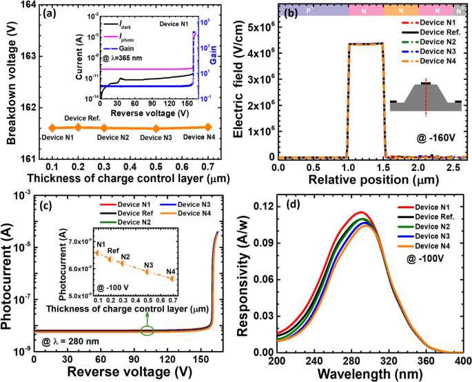
一 击穿电压,b SACM APD 的垂直电场分布偏置在 − 160 V, c 280 nm光照下的光电流-电压特性,以及d 对于参考器件和具有不同电荷控制层厚度的器件 N1 至 N4,SACM APD 的光谱响应特性分别偏置在 - 100 V。 a 中的插图 显示了计算出的电流-电压特性和器件 N1 的倍增增益。 c 中的插图 显示参考器件和器件 N1 至 N4 的光电流偏置在 - 100 V
电荷控制层的作用是将强电场和载流子倍增过程限制在倍增层内。然而,只要电荷控制层中的掺杂浓度降低,耗尽区宽度可以进一步扩大。然后电场分布可以显着影响击穿电压、光生电流、增益和响应度。因此,我们设计了表 3 中的器件 C1 到 C4。根据图 8a,随着掺杂浓度的降低,击穿电压最初保持不变,然后当电荷控制层的掺杂浓度低于 2 时击穿电压增加× 10 18 厘米 −3 .图8a的插图表明器件C1的击穿电压为~ 315 V,而暗电流也上升到3.5 × 10 -11 A 与设备 N1 的比较。为了揭示图 8a 中观察的起源,我们计算了图 8b 中的垂直电场分布,这表明电场主要集中在参考器件和器件 C3 和 C4 的倍增层中。然而,当电荷控制层的掺杂浓度低于2 × 10 18 时,电场和耗尽区会穿透电荷控制层。 厘米 −3 .器件C1和C2耗尽区的扩大有助于降低电场强度,因此器件C1和C2的击穿电压相应增加。增加的耗尽区宽度会产生更多的空间电荷产生电流,从而导致暗电流增加,即 3.5 × 10 - 11 A 和 5 × 10 − 11 A 分别用于设备 C1 和 C2。然后,我们在图 8c 中显示了 280 nm 波长处的光生电流。 The 100V-biased spectral responsivity curves at different wavelengths for the five investigated devices are illustrated in Fig. 8d. Excellent agreement is obtained between Figs. 8c and d, such that the increased photo-generated current gives rise to the enhanced responsivity, i.e., devices C1 and C2. Other devices show similar photo-current level and the responsivity.

一 Breakdown voltage, b vertical electric field distribution of the SACM APDs biased at − 160 V, c photocurrent biased at − 100 V, and d spectral response characteristics of the SACM APDs biased at − 100 V for reference device and devices C1 to C4 with different doping concentration of charge control layer, respectively. Inset figure in a shows the calculated current-voltage characteristics and the multiplication gain for device C1. Inset figure in c shows photocurrent-voltage characteristics for reference device and devices C1 to C4
As has been interpreted previously, the energy band barrier height at the interface of multiplication layer/charge control layer can soundly affect the carrier diffusion. Due to the expansion of the depletion region for devices C1 and C2, the electric field in the depletion region will annihilate the energy barrier at the interface of multiplication layer/charge control layer [e.g., the inset for device C1 in Fig. 9a]. Meanwhile, we observe the valence band barrier at the interface of multiplication layer/charge control layer for device C4 according to the inset for Fig. 9b. The energy barrier will correspondingly retard the hole diffusion into the multiplication layer from the charge control layer. We also selectively compute and show the hole concentration profiles for device C1 and C4 in Fig. 9c. Because the interface of multiplication layer/charge control layer for device C1 no longer hinders the injection of photo-generated holes into the multiplication layer, more holes are limited in the charge control layer and the absorption layer for device C4. As a result, the hole concentration in the multiplication layer for device C1 is higher than that for device C4. Thus, the enhanced photo-generated current and the responsivity for device C1 are obtained when compared with device C4.

Energy band diagrams for a device C1 and b device C4, c hole concentration profiles for device C1 and C4. Data are calculated at the reverse voltage of 100 V. Insets for a and b show the local energy band diagrams for multiplication layer/charge control layer for devices C1 and C4, respectively
Impact of the Structural Parameters for the Multiplication Layer on the Photoelectric Performance
The impact ionization and the carrier multiplication process take place in the multiplication layer, making the design for the multiplication layer essentially vital for 4H-SiC SACM APDs. Therefore, we look into the impact of the thickness and doping concentration for the multiplication layer on the photoelectric performance for SACM APDs. The detailed structural information of the multiplication layer for different SACM APDs are summarized and presented in Table 4. The only difference for the devices in Table 4 lies on the multiplication layer.
As Fig. 10a presents, the breakdown voltage is enhanced from 110 to 210 V when the multiplication layer thickness is increased from 0.3 to 0.7 μm. For the purpose of demonstration, the inset of Fig. 10a demonstrates the current in terms of the voltage for reference device and devices P1 to P4. This indicates that a thick multiplication layer helps to reduce the electric field intensity [see Fig. 10b] and increase the breakdown voltage. We then show the photo-generated current for the five devices in Fig. 10c. The photo-generated current increases slightly with increasing the thickness of the multiplication layer for devices P2 to P4, except that device P1 has the highest photocurrent. The spectral responsivity characteristics for the five investigated devices at the reverse voltage of 100 V are provided in Fig. 10d. The peak responsivity for reference device and devices P2 to P4 improves slightly as the thickness of the multiplication layer increases, and this is because the number of carriers generated by impact ionization increases when the depletion region width increases. Note that device P1 with the thinnest multiplication layer owns the highest peak responsivity at the wavelength of 280 nm. This is because the − 100 V applied voltage is close to Geiger mode for device P1, and the avalanche gain is more likely to occur than that for other devices.

一 Breakdown voltage, b vertical electric field distribution of the SACM APDs biased at − 160 V, c photocurrent biased at − 100 V, and d spectral response characteristics of the SACM APDs biased at − 100 V for reference device and devices P1 to P4 with different thicknesses of multiplication layer, respectively. Inset figure in a shows the calculated current-voltage characteristics for reference device and devices P1 to P4. Inset figure in c shows photocurrent-voltage characteristics under 280 nm illumination for reference device and devices P1 to P4
Then, we show the breakdown voltage in terms of the multiplication layer doping concentration for reference device and devices D1 to D4 in Fig. 11a. It seems that when the doping concentration for the multiplication layer is lower than 10 16 厘米 −3 , the breakdown voltage is less affected. We believe the breakdown voltage can be significantly decreased if the doping concentration in the multiplication layer exceeds 10 18 厘米 −3 . The dark current as a function of the applied bias for the five APDs are shown in the inset of Fig. 11a. The dark current increases with increasing doping concentration of the multiplication layer due to the enhanced space charge generation in the depletion region. Therefore, for the purpose of significantly decreasing the dark current and promoting the carrier multiplication process, we rarely have the multiplication layer heavily doped. Then, we calculate the vertical one-dimensional electric field profiles for the five studied devices, which are demonstrated in Fig. 11b. We can see that the electric field profiles of the five devices are mainly confined in the multiplication layer. In addition, Figs. 11c and d demonstrate the photo-generated current and the wavelength-dependent responsivity for the five devices. We can see that the photo-generated current for reference device and devices D1 and D2 are almost the same under the 280 nm illumination, while that the photon-generated current for the devices D3 and D4 is slightly increased. Therefore, the responsivity at the wavelength of 280 nm in Fig. 11d for devices D3 and D4 is slightly higher than the others.

一 Breakdown voltage, b vertical electric field distribution of the SACM APDs biased at − 160 V, c photocurrent-voltage characteristics under 280 nm illumination, and d spectral response characteristics of the SACM APDs biased at − 100 V for reference device and devices D1 to D4 with different doping concentration of multiplication layer, respectively. Inset figure in a shows the calculated current-voltage characteristics for reference device and devices D1 to D4. Inset figure in c shows photocurrent for reference device and devices D1 to D4 biased at − 100 V
Impact of the Beveled Mesa Angle on the Photoelectric Performance
In order to eliminate premature breakdown and suppress leakage current that are caused by the junction termination, positive beveled mesas with a small inclination angle are usually adopted when fabricating 4H-SiC APDs [13,14,15,16, 18]. However, the angles of the positive beveled mesa adopted in previous reports are various. Thus, to get systematic insight into the influence of different mesa inclination angles on the electric field profiles for 4H-SiC SACM APDs, we design the devices that are shown in Table 5.
We firstly calculate and show the dark current-voltage characteristics for the six investigated devices with the various bevel angles in Fig. 12a. We can see that the dark current increases as the positive beveled angle becomes large [see Fig. 12a]. The breakdown voltages for the investigated devices are ~ 161.6 V except that device E5 is slightly less than 161.6 V. The premature breakdown is observed as the beveled mesa angle increase in the dark condition. Meanwhile, we calculate and show photo-generated current in terms of the applied bias for reference device and devices E1 to E5 in Fig. 12b. We also see that the photo-generated current also increases as the positive bevel increases according to the inset for Fig. 12b. The premature breakdown is also observed as the beveled mesa angle increase in Fig. 12b. Therefore, the responsivity of solar-blind waveband at − 100 V slightly enhances as the positive bevel angle increases according to Fig. 12c.

一 Numerically calculated dark current-voltage characteristics, b photocurrent-voltage characteristics under 280 nm illumination, and c spectral response characteristics of the SACM APDs biased at − 100 V for reference device and devices E1 to E5, respectively
To reveal the origin for the observations in Figs. 12a and b, we calculate the lateral electric field distribution in the multiplication layer at the reverse bias of − 100 V in Fig. 13a, which demonstrates that, when the beveled mesas are utilized, the electric field decreases from the mesa center to the mesa edge. Moreover, the edge electric field intensity drops as the angle further decreases for the investigated devices. As has been mentioned, the junction termination will cause a large number of surface imperfections, which may cause the premature breakdown and the strongly leakage current, and the adopting of the beveled mesa shifts the premature breakdown from the mesa surface to the bulk [29]. Moreover, to get a full picture for the electric field profiles, the two-dimensional electric field distributions at the reverse bias of − 100 V for reference device and devices E1 to E5 are presented in Figs. 13b-g. We can see that the area of the high electric field in the entire multiplication layer gets narrowed, and this simultaneously causes the carriers that regenerated by impact ionization to decrease. As can be seen from Table 6, as the beveled mesa angle decreases, the surface electric field at the relative position of 700 μm decreases from 2.03 × 10 6 V/cm to 2.90 × 10 5 V/cm. As a result, the surface leakage and bulk leakage can be further suppressed as the beveled mesa angle get further decreased as shown in Fig. 12a. Although a small beveled mesa angle is preferred, this sacrifices the active detection area for APDs, and therefore, the responsivity is the lowest for device E1 according to Fig. 12c. Thus, one shall properly optimize beveled mesa angles depending on the crystalline quality for the 4H-SiC epitaxial layers and the surface conditions after junction termination. The suggested beveled angle in this works is in the range of 10–20°.

一 Lateral electric field distribution of the multiplication layer at − 100 V, and numerically calculated two-dimensional electric field distribution at − 100 V for b device E1, c reference device, d device E2, e device E3, f device E4 and g device E5
结论
To summarize, we have numerically investigated and demonstrated the impact of the thickness and doping concentration of each layer on photoelectric performance for 4H-SiC SACM APDs. The obtained conclusions are as follows:(1) for n-type ohmic contact layer with a properly high doping concentration (N d ≈ 1 × 10 19 厘米 −3 ) to enable ohmic contact, the thickness and doping concentration hardly affect the breakdown voltage. Nevertheless, the responsivity decreases as the thickness of the n-type ohmic contact layer increases. The thickness shall be controlled to about 0.2 μm; (2) the doping concentration for the absorption layer is vitally important, which can modulate the photo-generated carrier transport and affect the responsivity. The doping concentration is generally controlled at the intrinsic concentration (N d ≈ 1 × 10 15 厘米 −3 ); (3) the doping concentration for the charge control layer regulates the electric field distribution and affects the depletion region width for 4H-SiC SACM APDs. The depletion region width increases as the doping concentration of the charge control layer decreases. According to our results, when the doping concentration is about 1 × 10 18 厘米 −3 , the depletion region can be completely terminated by the charge control layer; (4) the breakdown voltage can be strongly affected by the thickness of multiplication layer which is the main support region of the electric field. The dark current is sensitive to the doping concentration of multiplication layer, and a low doping concentration for the multiplication layer is required, since the doping concentration therein influences the space charge generation current. Thus, the suggested doping concentration in this works is intrinsic concentration (N d ≈ 1 × 10 15 厘米 −3 ); (5) we also point out the advantage of beveled mesa for 4H-SiC SACM APDs, and the optimized beveled mesa angles shall be a compromise among the active detection area, the surface conditions for the mesa, and the crystalline quality for 4H-SiC epitaxial films. This work indicates that the optimum beveled mesa angle is in the range of 10–20°. We strongly believe that this work provides the physical insight for the device physics and hence the findings in this work are very important for 4H-SiC-based SACM APDs.
数据和材料的可用性
The data and the analysis in the current work are available from the corresponding authors on reasonable request.
缩写
- AlGaN:
-
Aluminum gallium nitride
- APSYS:
-
Advanced Physical Models of Semiconductor Devices
- MSM:
-
Metal-semiconductor-metal
- SACM:
-
Separated absorption charge and multiplication
- SiC:
-
Silicon carbide
- SRH:
-
Shockley-Read-Hall
- UV APD:
-
Avalanche ultraviolet photodiode
纳米材料
- 修复损坏的维护策略:PM 优化和 FMEA
- 用于灵敏快速检测卵巢癌细胞的柔性石墨烯生物传感器的演示
- 用于 Micro-LED 和 VCSEL 的高级原子层沉积技术
- 三态电致变色器件的浸涂工艺工程和性能优化
- 用于高效偏振分束器和光学涡流发生器的高阶介电超表面
- 螺旋型天线微桥结构太赫兹微测辐射热计的调频和吸收改进
- 具有专门设计的超晶格 p 型电子阻挡层以实现高 Mg 掺杂效率的几乎无效率下降的基于 AlGaN 的紫外发光二极管
- 铌酸锡光催化剂的转向电荷动力学:相结构和电子结构的关键作用
- 关于用于基于 AlGaN 的深紫外发光二极管的 p-AlGaN/n-AlGaN/p-AlGaN 电流扩展层
- 用于高能量转换效率的接触式摩擦纳米发电机理论系统
- 高压PCB材料和设计
- VMC Machinery 用于生产和提高效率