

三态电致变色器件的浸涂工艺工程和性能优化
摘要
通过浸涂技术将二氧化钛 (TiO2) 纳米颗粒改性到掺氟氧化锡 (FTO) 上,该技术具有不同的纳米颗粒尺寸、提升速度、前体浓度和浸渍次数。随后通过在改性 FTO 电极和平面 FTO 电极之间夹入适量的凝胶电解质,制备具有可逆三态光学转换(透明、镜面和黑色)的基于电沉积的电致变色器件。研究了浸涂工艺工程、TiO2 薄膜的形态特征(即厚度和粗糙度)以及电致变色器件的性能(即光学对比度、切换时间和循环稳定性)之间的相关性。通过调整浸涂工艺工程,改进后的器件表现出 57% 的高光学对比度、6 秒和 20 秒的短着色/漂白切换时间以及在 1500 次循环后仅降低 27% 衰减率的优异循环稳定性。本研究结果将为合理设计性能令人满意的电致变色器件提供有价值的指导。
背景
电致变色材料的一个吸引人的特点是在施加电压时能够以可逆和持久的方式改变其光学特性。自 Deb [1] 的开创性工作以来,已经开发出多种电致变色材料,可分为几个子集:过渡金属氧化物 [2]、普鲁士蓝 [3]、导电聚合物 [4]、紫罗碱 [5] 、过渡金属离子配位化合物 [6]、混合电致变色材料 [7] 和基于可逆电沉积的电致变色材料 [8, 9]。它们的电致变色性能,包括光学对比度、切换时间、着色效率、循环稳定性和光记忆效应等得到了广泛的研究,这促使我们扩大电致变色材料在智能窗、防眩后视镜、电致变色显示器、电子纸和军用伪装 [10,11,12,13,14,15,16,17,18,19]。基于可逆电沉积的电致变色器件由于其简单的夹心式结构以及简便和低成本的制造,在光调制中的应用前景广阔。它们的光学特性可以通过在施加电压和溶解作用下将金属(铜 (Cu)、铋 (Bi)、铅 (Pb)、镍 (Ni)、银 (Ag) 等)沉积到透明导电电极上来控制去除电压后金属回到电解液中 [20,21,22,23,24,25,26]。铋铜 (Bi/Cu) 电沉积器件由于 Bi 和 Bi 3+ 之间的氧化还原而在黑色和透明状态之间快速可逆地转换,因此被广泛用于信息显示 [9, 23,24,25]。同样,基于银的电沉积系统 [26,27,28,29] 也被开发用于制造电致变色器件,因为它具有实现镜面状态的能力。
通常,由于改性电极表面对光的吸收和/或多次散射,适当的电极表面改性可能会触发基于电沉积的电致变色装置的可逆和多色状态 [30,31,32,33]。各种技术,包括溅射[34]、真空蒸发[35]、化学气相沉积[36]、水热[37]、电沉积[38]和溶胶-凝胶[39、40],已被用于制造电致变色薄膜.在各种技术中,溶胶-凝胶方法因其成本低、适合大面积制备和易于处理的特性而具有优势,其中旋涂和浸涂技术被广泛使用。与旋涂相比,浸涂技术由于其更高的可控性和更适用于大规模制备而成为首选[24]。此外,迪帕等人。 [24] 还报道了基于三氧化钨 (WO3) 薄膜的浸涂电致变色器件与旋涂器件相比表现出优异的性能,例如改进的透射调制、着色效率、切换速度和着色/漂白循环。然而,浸涂技术尚未应用于制备基于电沉积的Ag/Cu电致变色器件。
基本上,电致变色材料的电致变色性能(即光学对比度、切换时间、着色效率、循环稳定性和光学记忆效应)基本上取决于它们的结构、表面形态和组成特性 [41]。因此,对电致变色材料性能改进的制备参数进行更仔细的检查是非常必要的。迪帕等人。 [42] 通过浸涂技术制造 WO3 薄膜,以及在草酸乙酰化过氧钨酸溶胶薄膜沉积过程中相对湿度 (RH) 变化(55% 和 75% RH)对 WO3 薄膜的微观结构和电致变色性能的影响退火后获得。在 75% RH 下制造的薄膜获得了更快的透明和蓝色状态之间的转换动力学、更大的锂嵌入电流密度、更高的锂扩散系数和优异的循环稳定性,表明湿度变化对电致变色材料的结构和电致变色性能。 Sun 和他的同事 [43] 通过溶胶-凝胶法结合旋涂法制备了 WO3 薄膜。研究了退火温度对WO3薄膜微观结构和光学性能的影响,在较低的退火温度下获得了可见光范围内更高的透射率调制。前体溶胶中有机部分的类型和含量、薄膜制备方法(旋涂或浸涂)对薄膜性能的影响也已得到广泛研究 [43, 44],以大致了解电致变色薄膜的电致变色性能和制备参数。荒木等人。 [41] 通过旋涂将银沉积到改性氧化铟锡 (ITO) 电极上,并获得可逆的黑色和镜面状态。 Tsuboi 及其同事 [42, 44] 通过控制不同电压下 Ag 晶粒的生长,进一步追求多种颜色状态,表明对纳米粒子尺寸和形状的操纵可以导致巨大的变化彩色。在我们之前的研究 [33] 中,我们制造了具有可逆三态光学转换(透明、黑色和镜面状态)的基于电沉积的 Ag/Cu 电致变色器件,并带有导电的 TiO2 纳米颗粒修饰的掺氟氧化锡 (FTO)。 ) 通过旋涂技术制造的电极。我们还证明了通过操纵 TiO2 修饰的 FTO 电极的表面结构可以有效地控制器件在不同状态下的光学特性。然而,关于电极表面改性对多态电致变色器件的影响的更仔细检查鲜有报道。因此,通过制备参数对基于电沉积的电致变色器件性能进行深入研究具有重要意义。
在这项研究中,TiO2 纳米粒子通过浸涂技术修饰到 FTO 上,然后将适量的凝胶电解质夹在修饰的 FTO 电极和平面 FTO 电极之间,以制造具有可逆三态光学转换的电沉积电致变色器件.由于浸涂技术的高度可控性,可以通过操纵电极表面改性来调节器件的光学性能。纳米颗粒尺寸是一个重要的参数,可以操纵并且可以使制造的设备的性能不同。因此,调整纳米颗粒尺寸以研究其对 TiO2 薄膜的微观结构和制造的器件性能的影响。除纳米颗粒尺寸外,提升速度、前体浓度和浸渍次数是浸涂过程中的主要参数。在此,还改变了提升速度、前驱体浓度和浸渍次数,以研究它们对 TiO2 薄膜微观结构以及电致变色器件性能的影响,即透射率/反射率、光学对比度、切换时间和循环稳定性.本研究结果将为合理设计性能令人满意的电致变色器件提供有价值的指导。
方法
材料
FTO透明导电玻璃,尺寸为25 × 30mm,厚度为2.2mm,方块电阻为10Ωsq -1 用作电极,其购自武汉莱迪思太阳能科技有限公司。平均直径为 5~10、40 和 100 nm(阿拉丁有限公司)的均匀 TiO2 纳米粒子用于修饰 FTO 电极。电解质化合物,包括二甲基亚砜(DMSO,≥99.8%,J&K Chemical Co. Ltd.),四-n -丁基溴化铵(TBABr,≥99%,J&K Chemical Co. Ltd.),硝酸银(AgNO3,≥99.8%,广东光华科技有限公司),氯化铜(CuCl2,≥99.0%,KeLong Chemical Co. Ltd.)有限公司),聚乙烯醇缩丁醛(PVB,积水化学有限公司),乙基纤维素(≥99.5%,汉州兰博实业有限公司),月桂酸(≥99.8%,科隆化工有限公司) 、萜品醇(≥98.0%,科隆化工有限公司)和乙醇(≥99.7%,科隆化工有限公司)均来自商业来源。所有溶剂和化学品均符合试剂质量,无需进一步纯化即可使用。将厚度为 0.5 毫米的特氟龙板(Aladdin Co. Ltd.)切割成 25 × 25 毫米,并带有 20 × 20 毫米的孔。 FTO玻璃电极和聚四氟乙烯片在使用前均用乙醇和去离子水清洗数次。
TiO2 纳米颗粒分散体和凝胶电解质的制备
为了制备二氧化钛纳米粒子分散体,首先将二氧化钛纳米粒子(原材料,2.5 克)与月桂酸(表面活性剂,0.25 克)和乙基纤维素(粘合剂,0.75 克)一起放入球磨罐中,并与松油醇(粘合剂)混合, 16 mL) 和乙醇(溶剂,10 mL),然后立即研磨。研磨 50 分钟后获得 TiO2 纳米颗粒浆料,然后用乙醇稀释该浆料。为了制备凝胶电解质,将 TBABr(806 毫克,2.5 毫摩尔)、硝酸银(85 毫克,0.5 毫摩尔)和氯化铜(13 毫克,0.1 毫摩尔)溶解在 10 毫升 DMSO 中,然后加入 PVB( 1.32 克,10 重量%)。最后,将混合溶液在暗处放置24~48 h,得到凝胶电解质。
FTO 电极的修改和电致变色器件的制造
采用浸涂技术对 FTO 透明导电电极进行改性,典型工艺如下:将作为稀释剂的乙醇(10、15 或 20 mL)加入到 TiO2 纳米颗粒分散体(5 mL)中,超声混合 30分钟随后,将整个背面和正面上贴有丝锥的 FTO 电极固定在浸涂机上,以 6000 μm/s 的速度浸入上述分散液中,并以 1000、2000 和 3000 μm/s 的速度提升, 分别。通过将制备的样品在 500°C 下烧结 30 分钟,获得 TiO2 纳米颗粒修饰的 FTO 导电电极。为了进行比较,使用了不同尺寸(5~10、40 和 100 nm)的 TiO2 纳米粒子,以及不同的浸涂参数,包括提升速度(1000、2000 和 3000 μm/s)、前体浓度(与本研究使用 TiO2 纳米颗粒分散体和 1:2、1:3 和 1:4 的乙醇以及浸渍次数(1、3 和 5)。具体而言,为了研究 TiO2 纳米颗粒尺寸对电致变色器件性能的影响,通过将提升速度固定为 3000 μm/s,使用尺寸为 5~10、40 和 100 nm 的 TiO2 纳米颗粒,前驱体浓度为1:2,浸渍次数为1。为了研究提升速度对电致变色器件性能的影响,通过将TiO2纳米颗粒尺寸固定为5~10,使用1000、2000和3000μm/s的提升速度nm,前驱体浓度为1:2,浸渍次数为1。 为了研究前驱体浓度对电致变色器件性能的影响,TiO2纳米颗粒分散体与乙醇的比例为1:2、1:3,和 1:4 通过固定 TiO2 纳米颗粒尺寸为 5~10 nm,提升速度为 3000 μm/s,浸渍次数为 1。为了研究浸渍次数对电致变色器件性能的影响,通过固定 t 使用了 1、3 和 5 的浸渍数TiO2 纳米颗粒尺寸为 5~10 nm,提升速度为 3000 μm/s,前驱体浓度为 1:2。为了组装基于电沉积的电致变色装置,基于 DMSO 的凝胶电解质包含在 20 毫米 × 20 毫米的密封方形空间中,在 0.5 毫米厚的聚四氟乙烯片内切割,并通过将聚四氟乙烯片夹在两个 FTO 电极之间进行密封(其中一个用TiO2纳米颗粒改性)。
特征化
使用场发射扫描电子显微镜(FESEM,S-3400,Hitachi)观察TiO2 纳米颗粒修饰的FTO 电极的形貌。通过使用原子力显微镜(AFM,Multimode V,Veeco)表征 TiO2 纳米颗粒修饰的 FTO 电极的粗糙度。使用电化学工作站(CHI660D,CHI)将转换电压施加到电致变色装置上,并使用紫外-可见分光光度计(Cary 5000,安捷伦)测量透射率和反射率光谱。通过使用双电极模式获得所有电致变色性能,包括光学对比度、切换时间和循环稳定性,负极和正极分别连接到扁平 FTO 电极和 TiO2 纳米颗粒修饰的 FTO 电极。测量时电致变色装置的对电极为扁平FTO电极,工作电极为TiO2纳米颗粒修饰的FTO电极。通过施加合适的电压,浸涂电致变色器件表现出三种可逆的光学状态,包括透明、镜面和黑色。
结果与讨论
通过在基于电沉积的电致变色器件上交替施加/去除合适的电压,可以实现镜面、黑色和透明状态之间的可逆三态光学转换。分别沉积在粗糙的 TiO2 纳米粒子修饰的 FTO 电极和平面电极上的 Ag 将触发黑色和镜面状态。因此,修改后的器件的黑色状态会受到其表面形态结构的强烈影响。为了研究 TiO2 薄膜的表面形态结构对改性器件性能的影响,通过球磨制备了三种含有不同尺寸(5~10、40 和 100 nm)的 TiO2 纳米颗粒的前驱体溶液。随后,通过浸涂技术将前体溶液涂覆到 FTO 电极表面,烧结处理,并在改性 FTO 电极和扁平 FTO 电极之间夹入适量的凝胶电解质,从而获得改性器件。首先,在 400 到 800 nm 的光谱范围内测量了三种改进器件在透明、镜面和黑色状态下的光学透射率和反射率光谱。对于透射率测量,电源的负极和正极分别连接到扁平 FTO 电极和 TiO2 纳米颗粒修饰的 FTO 电极,20 秒后产生 +2.5 V 的镜面状态和 -2.5 V 的黑色状态。对于反射率测量,施加相同的电压 90 秒。在透明状态下,分别用 5~10、40 和 100 nm 的 TiO2 纳米粒子制备的改性器件观察到 61%、50% 和 46% 的透射率(图 1a-c)。在黑色状态下,用 5~10 nm 的 TiO2 纳米粒子制备的改进装置显示出 15% 的最大透射率,当将 TiO2 纳米粒子的尺寸增加到 100 nm 时,透射率降低到 10%(图 1a-c)。在镜面状态下,用 5~10 nm 的 TiO2 纳米粒子制备的改进装置显示出与 40 和 100 nm 相似的透射率(图 1a-c)。光学对比度通常定义为电致变色装置在其着色和漂白过程之间的透射率、反射率或吸光度的最大差异。通过计算器件在透明和黑色状态之间的透射率差异,可以获得 48%、42% 和 39% 的光学对比度。随着 TiO2 纳米颗粒尺寸的增加,光学对比度的降低主要归因于器件在透明状态下的透射率降低。用 5~10 nm TiO2 纳米粒子制备的改进装置的反射峰与用 40 和 100 nm TiO2 纳米粒子制备的反射峰不同,峰值位置分别位于 700、750 和 750 nm(图 1d-f)。基本上,折射率通常由材料、结构(即膜的数量和排列)、厚度和膜的界面形态/结构决定。因此,镜面状态下基于电沉积的改性电致变色器件的波长相关反射光谱出现峰移的原因可能是不同的 TiO2 纳米颗粒尺寸、TiO2 薄膜厚度和 TiO2 薄膜的综合影响。表面粗糙度 [45,46,47]。此外,在镜面状态下的修改后的器件中观察到超过 70% 的反射率,在黑色和镜面状态下的三个修改后的器件中观察到 20% 的低反射率(图 1d-f)。需要注意的是,上述数值并不对应于所能达到的最暗状态。上述结果表明,沉积在透明电极上的TiO2纳米颗粒的尺寸可以改变电沉积器件的透光率、光反射率和光学对比度。
<图片>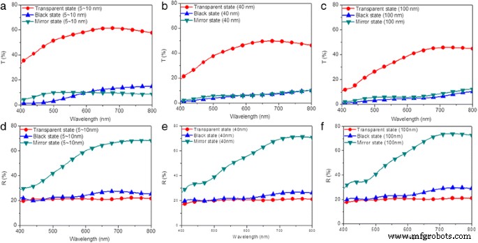
(Color online) 基于电沉积的电致变色器件在透明(红色 ), 黑色 (蓝色 ) 和镜像状态 (green )。用a制备的修饰器件的透射光谱 5~10,b 40 和 c 分别为 100 纳米。用d制备的改进器件的反射光谱 5~10,e 40 和 f 分别为 100 纳米
研究了不同纳米粒径的浸涂二氧化钛薄膜的结构特征。在 2θ 范围从 20° 到 80° [33, 48]。如附加文件 1 所示:图 S1a,制备的 TiO2 薄膜、烧结的 TiO2 薄膜和未经进一步处理的新鲜 5~10 nm TiO2 纳米颗粒的衍射峰出现在相同位置,并且与 TiO2 的锐钛矿结构形式非常匹配(TiO2锐钛矿,JCPDS 21-1217)。这些值与文献数据非常吻合 [48],与锐钛矿相的晶面 (101)、(004)、(200)、(105)、(211) 和 (204) 对应出现加宽的色散峰.在 52° 和 62° 处观察到的额外峰来自 FTO 电极表面,这与氧化锡的结构形式 (SnO2, JCPDS 46-1088) [33, 49] 非常匹配。在烧结前后,40 和 100 nm TiO2 纳米颗粒修饰的 FTO 电极也观察到了类似的锐钛矿结构形式(附加文件 1:图 S1b 和 S1c)。可以看出,浸涂的 TiO2 薄膜在整个 FTO 电极改性制备过程中保持与新鲜 TiO2 纳米粒子相同的结构形式,表明浸涂的 TiO2 薄膜的结构特征不会受到浸渍的影响。涂层方法,我们之前的报告[33]也给出了类似的结果。
其次,研究了三种浸涂二氧化钛薄膜的形态特征。图 2 提供了在 Ag 沉积之前浸涂的 TiO2 薄膜的照片、面内和横截面 SEM 图像。使用 TiO2 纳米颗粒沉积的 FTO 电极显示出不同的透明度,并在增加 TiO2 纳米颗粒的尺寸后逐渐模糊(图 2a-c)。用 5~10 nm 的 TiO2 纳米粒子制备的薄膜显示出晶粒之间清晰明确的边界以及孔和晶粒的均匀分布,表明获得了均匀且细粒度的 TiO2 薄膜(图 2d)。然而,在增加 TiO2 纳米颗粒的尺寸后,沉积的 TiO2 薄膜的表面变得粗糙和不均匀(图 2e、f)。 TiO2 纳米粒子的这种不均匀分布主要是由于它们在浸涂和烧结过程中在乙醇中的分散性和团聚逐渐降低。随着纳米颗粒尺寸的增加,逐渐模糊和更粗糙的 TiO2 薄膜说明修改后的器件的透射光谱降低,如图 1a 所示。通常,通过横截面SEM图像测量三种TiO2薄膜的厚度增加,对于用5~10、40和100制备的FTO电极,TiO2薄膜的厚度为320、409和612nm分别观察到纳米二氧化钛纳米粒子。在浸涂过程中,通过溶剂蒸发过程中颗粒重力、提升力和毛细管力之间的平衡,可以获得连续的薄膜。由于不同的颗粒重力和毛细管力,预计不同的纳米颗粒尺寸会产生不同的平衡力,从而导致不同的厚度和粗糙度。如图 1a、b 所示,在增加 TiO2 纳米颗粒尺寸后,透明状态下改性器件的透射率、反射率和光学对比度发生了变化。由此可见,TiO2纳米颗粒尺寸增大导致透明状态下改性电致变色器件透光率降低的主要原因是浸涂TiO2薄膜的厚度增加。
<图片>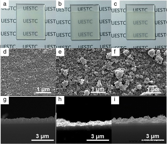
(彩色在线)用 a 的纳米颗粒制备的 TiO2 薄膜的照片 5~10,b 40 和 c 分别为 100 纳米。纳米粒径d制备的TiO2薄膜的面内SEM图像 5~10,e 40 和 f 分别为 100 纳米。 g纳米颗粒制备的TiO2薄膜的横截面SEM图像 5~10, h 40 和 i 分别为 100 纳米
通过使用原子力显微镜(AFM)进一步测量三个浸涂的 TiO2 薄膜的粗糙度,如图 3a-c 所示。浸涂的 TiO2 薄膜的粗糙度作为纳米颗粒尺寸的函数绘制在图 3d 中,用 5~10、40 和 100 nm TiO2 制备的 TiO2 薄膜的粗糙度为 39、117 和 142 nm分别测量了纳米颗粒。观察到粗糙度增加是由于较大的 TiO2 纳米颗粒更多的聚集和更低的分散性。基本上,透射率和相关反射率用于描述入射到设备的波的行为。折射率因子是一个必不可少的指标,由膜的材料、结构(即膜的数量和排列)、厚度和界面形态/结构决定。在研究具有不同尺寸 TiO2 纳米粒子的基于电沉积的改性电致变色器件的光学特性时,应考虑所有上述因素。触发修改后的器件的黑色状态后,所有 FTO 表面都变成深黑色,表明 Ag 层显着修改了 FTO 电极的表面形态(附加文件 1:图 S2a、S2b 和 S2c)。具有沉积 Ag 层的改良器件的所有 FTO 表面都比涂有光头 TiO2 薄膜的器件表面更光滑(附加文件 1:图 S2d、S2e 和 S2f)。浸涂的 TiO2 薄膜的横截面 SEM 图像(附加文件 1:图 S2g、S2h 和 S2i)也显示出所有三种改进器件的厚而致密的 Ag 沉积层。如图 1 所示,Ag 沉积后透射率和反射率光谱发生变化,器件转变为黑色状态,表明厚度和粗糙度对透射率和反射率的影响很大。应考虑改变膜结构的综合影响,包括额外沉积的Ag层、改变的厚度和顶层的界面形态。
<图片>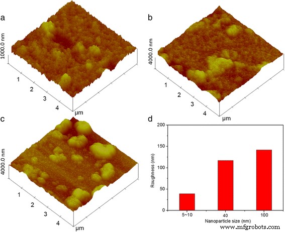
(彩色在线)纳米粒径a制备的TiO2薄膜的AFM图像 5~10,b 40 和 c 100 纳米和 d TiO2薄膜粗糙度与TiO2纳米颗粒尺寸的关系
第三,在两电极循环伏安 (CV) 测试期间测量了三个改进器件在 700 nm 处的时间相关透射率变化,连续四个着色/漂白循环和 100 mV/s 的扫描速率。对于透射率测量,+2.5 和 -2.5 V 的电压交替施加到 TiO2 修饰的 FTO 电极上 20 秒。图 4 显示了使用不同尺寸的 TiO2 纳米粒子制备的改进装置的透射率随时间的变化。用 5~10、40 和 100 nm TiO2 纳米粒子制备的改性器件的初始透光率在漂白时分别达到 61、50、46%,在着色时分别降至 34、25、18%。基本上,着色过程意味着设备从透明状态变为镜面/黑色状态,漂白过程意味着设备从镜面/黑色状态反向变为透明状态。着色/漂白切换时间表示为在着色和漂白过程中达到其最大调制的 90% 所需的时间。对于用不同尺寸的 TiO2 纳米粒子改性的器件,测量了不同的切换时间,其中用 5~10 nm TiO2 纳米粒子制备的改性器件在着色和漂白过程之间表现出最短的切换时间(着色 6 秒,漂白 20 秒)。随着纳米颗粒尺寸的增加,转换时间增加说明用更薄和更光滑的 TiO2 薄膜改性的 FTO 电极有助于更短的着色/漂白转换时间。此外,漂白过程比所有设备的着色过程都慢,大多数关于电致变色设备的文章都说明了这一点。此外,修改后的器件从透明状态转变为镜面状态的时间比器件从透明状态转变为黑色状态的时间短,表明沉积在 FTO 电极上的粗糙 TiO2 薄膜会影响其转换时间。此外,多孔过渡金属氧化物薄膜加工的最新进展为构建具有增强性能的电致变色器件开辟了新的机遇。例如,Zhang 等人报道,与致密膜相比,使用自组装单层聚苯乙烯 (PS) 球体作为模板在 ITO 玻璃上电沉积的周期性碗状大孔 WO3 阵列膜显示出更快的着色时间,为 3.6 秒在没有 PS 模板的情况下制备 [50]。 Yang 及其同事报道了通过模板辅助溶胶-凝胶法制备有序大孔 WO3 薄膜。获得的着色时间为 5.19 秒,明显短于致密薄膜的着色时间,即 6.9 秒 [51]。他们还证明了电致变色响应时间实际上受到离子扩散系数和扩散路径长度两个因素的限制,前者取决于化学结构,而后者取决于微观结构。
<图片>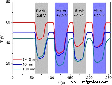
(在线颜色)在两电极 CV 测试期间获得的 700 nm 透射率变化,用于使用 5~10 的 TiO2 纳米颗粒(红色 ), 40 (蓝色 ) 和 100 纳米(绿色 ),分别
着色效率,CE (cm 2 /C ),是常用于评估电致变色器件的最佳参数之一。 CE 定义为每单位注入/提取电荷的光密度 (ΔOD) 变化 (Q )在某一波长[17],可由下式计算
$$ \mathrm{C}\mathrm{E}\left(\lambda \right)=\Delta \mathrm{O}\mathrm{D}\left(\lambda \right)/ Q =\log \left( T \mathrm{b}/ T\mathrm{c}\right)/ Q $$其中 ΔOD 是光密度的变化,Q (C /cm) is the charge injected per unit electrode area of the thin film, and T b and T c are the transmittance in the bleached and the colored states, respectively. The coloration efficiency of the modified devices prepared with 5~10, 40, and 100 nm TiO2 nanoparticles were listed in Additional file 1:Table S1. CE of 27.0, 20.7, and 16.9 cm 2 /C at 700 nm were obtained for modified devices prepared with 5~10, 40, and 100 nm TiO2 nanoparticles, respectively. The decreased CE value indicates that the modified devices prepared with 5~10 nm exhibits a large optical modulation with a small intercalation charge density. This decreased CE of the electrochromic devices may be due to the increased TiO2 nanoparticle size and TiO2 thin film thickness and roughness, as demonstrated by previous reports [52,53,54].
Generally, device failure occurs after repeatedly switching an electrochromic device between its coloration and bleached states for hundreds or thousands of times. This attributes to the combined effect of various side reactions including transparent electrode failure, electrolyte depravation, and active layer decay. Thus, cycling stability of the modified devices is further investigated by repeatedly applying sequential voltages. As shown in Fig. 5, transmittance variation of the three modified devices at 700 nm was measured by applying voltages of −2.5 V. Every 500 cycles was taken as a measurement node to measure the transmittance deviation of modified devices over time. The measured transmittance of the three devices are all below 1% and maintain fairly stable after the devices transferred into black state and the voltage removed for the first cycle. The transmittance of the modified devices in transparent states gradually decrease and increase for coloration states with the time and the cycle numbers, indicating more cycles lead to poorer stability. The optical contrast of the modified device prepared with 5–10 nm TiO2 nanoparticles decreases from 48 to 35% after 1500 cycles (Fig. 5a). As shown in Fig. 5b, c, the optical contrasts of modified devices prepared with 40 and 100 nm TiO2 nanoparticles decrease to 23 and 16%, respectively, indicating that the cycling stability can be improved by decreasing the size of TiO2 nanoparticles. To investigate the trace of Ag dissolution in the electrolyte for the sample with less stability, the morphological features of the dip-coated TiO2 thin film after manifold cycles were investigated. The SEM of dip-coated 100 nm TiO2 thin film after 1500 cycles was presented in Additional file 1:Figure S3. As shown in Additional file 1:Figure S3, uneven electrolyte agglomeration is observed for the dip-coated TiO2 thin film in our work, which is similar to that of the previous reports [55, 56]. Moreover, extra Ag was detected via energy-dispersive spectrometer (EDS) in the dip-coated TiO2 thin film after the transformation of modified device to the transparent state, with the results listed in the Additional file 1:Table S2. We supposed that the ability to achieve complete reversibility is deteriorated due to the gradual deposition of Ag onto bumps of TiO2 thin films and inability to dissolve Ag back into electrolyte immediately during the continuous cycling between the coloration and bleaching states. Thus, the improved cycling stability might be owed to the decreased surface roughness of TiO2 thin film, which is conducive to the quick dissolution of Ag back into electrolyte during the switching between the coloration and bleaching states, and the surface roughness of TiO2 thin film is strongly influenced by the TiO2 nanoparticle size. Therefore, both the particle size itself and the surface roughness are related to the improved cycling stability.

(Color online) Transmittance variation for dip-coated devices prepared with TiO2 nanoparticles of a 5–10, b 40, and c 100 nm, respectively, in transparent (black ) and black (red ) states at 700 nm after applying a sequence of voltages in the following order:−2.5 V (10 s), 0.5 V (30 s), 2.5 V (10 s), 0.5 V and (20 s), with each of the 500 cycles taken as a measurement node
In summary, improved optical contrast, switching time, and cycling stability were obtained with the decrease of TiO2 nanoparticle size, indicating that the effect of nanoparticle size on the electrochromic device is obvious in this work. By characterizing the SEM and AFM images of different-sized TiO2 thin film, increased thickness and roughness of the dip-coated TiO2 thin film are exhibited with the increase of TiO2 nanoparticle size, which results to the varied properties of electrochromic device, indicating the strong relevance between the TiO2 nanoparticle size and the morphological feature of the dip-coated TiO2 thin films. To effectively distinguish the effect of TiO2 nanoparticle size and TiO2 thin film morphological feature on the properties of modified electrochromic device, TiO2 thin films were deposited onto FTO electrodes under different modification conditions, including lifting speed, precursor concentration, and dipping number, by fixing the TiO2 nanoparticle size to 5~10 nm. The thickness and roughness of TiO2 thin films prepared with different lifting speeds, precursor concentrations, and dipping numbers were plotted in Fig. 6. To compare the effects of different lifting speeds, lifting speeds of 3000, 2000, and 1000 μm/s were used to deposit TiO2 nanoparticles onto the FTO electrodes, with nanoparticle size of 5~10 nm, ratios between TiO2 nanoparticle slurry and absolute ethyl alcohol of 1:2, and dipping number of 1. Figure 6a shows that the increase of lifting speed leads to the increased thickness and decreased roughness of the modified electrodes. To compare the effects of different precursor concentrations, ratios between TiO2 nanoparticle slurry and absolute ethyl alcohol of 1:2, 1:3, and 1:4 were used to modify the FTO electrodes, with nanoparticle size of 5~10 nm, lifting speed of 3000 μm/s, and dipping number of 1. The result in Fig. 6b reveals that the decrease of precursor concentration causes the decreased thickness and roughness of the modified electrodes. To compare the effects of different dipping numbers, dipping numbers of 1, 3, and 5 were used to prepare the modified electrode, with nanoparticle size of 5~10 nm, lifting speed of 3000 μm/s, and ratios between TiO2 nanoparticle slurry and absolute ethyl alcohol of 1:2. The increase in both roughness and thickness are observed with the increase of dipping number, as indicated in Fig. 6c.

(Color online) Roughness (red ) and thickness (black ) of TiO2 thin films prepared with a different lifting speeds, b precursor concentrations, and c dipping numbers provided
In addition, the morphological features of dip-coated TiO2 thin films on modified electrodes prepared under different electrode modification conditions before Ag deposition were observed. Figure 7 shows the in-plane SEM images of modified FTO electrodes under different modification conditions, including lifting speed, precursor concentration, and dipping number. Compared with SEM image of TiO2 thin film dip-coated with 3000 μm/s, more agglomeration of TiO2 nanoparticles are observed for TiO2 thin films prepared under lower lifting speed (Fig. 7a, b). The increase in agglomeration of TiO2 nanoparticles leads to the increased roughness for lower lifting speed, as illustrated in Fig. 6a. SEM images with higher magnification are inserted in the upper-right corner for each low-magnification SEM image. Both the TiO2 thin films prepared with 2000 and 1000 μm/s show uniform distribution of pores and grains with sharp and well-defined boundaries between grains (Fig. 7a, b). As shown in Fig. 7c, d, slight agglomeration of TiO2 nanoparticles are also observed for TiO2 thin films with lower precursor concentration and with same roughness as that prepared with 3000 μm/s obtained (Fig. 2a). Furthermore, the higher magnification SEM images for TiO2 thin films prepared under lower precursor concentration also show compact TiO2 thin film surfaces. Moreover, the SEM images of TiO2 thin films prepared with different dipping numbers are also presented in Fig. 7e, f, with a large amount of TiO2 nanoparticle agglomeration observed at higher magnification. A lot of pores are exhibited for TiO2 thin films prepared by repeating dipping number, with more repeating times lead to more pores. Thus, it can be seen that the effects of nanoparticle size, lifting speed, precursor concentration, and dipping number on the roughness of dip-coated TiO2 thin films are different, which gets us thinking about that both the dispersity in ethyl alcohol and dip-coating processes will influence the resulted roughness. Therefore, it is essential to investigate the effects of the process engineering on morphological features of dip-coated TiO2 thin films. As aforementioned, there are strong correlations between optical properties of modified device and morphological features of dip-coated TiO2 thin films. Therefore, the optical properties for the electrodeposition-based electrochromic device, including transmittance and reflectance spectra, optical contrast, switching time, and cycling stability, should be further investigated.

(Color online) SEM images of modified FTO electrodes under different fabrication conditions, including a lifting speed of 2000 μm/s, b lifting speed of 1000 μm/s, c precursor concentration of 1:3, d precursor concentration of 1:4, e dipping number of 3, and f dipping number of 5
Optical transmittance of devices modified under different electrode modification conditions in three states were measured in the spectra range of 400 to 800 nm, as shown in Fig. 8. For modified devices prepared with different lifting speeds (2000 and 1000 μm/s), the transmittance of the device in the transparent state was decreased with increased lifting speed, as a result of the increased thickness of TiO2 thin film (Fig. 8a, b). As for the black and mirror states, limited variations are observed for modified devices prepared with 2000, 1000, and 3000 μm/s, as illustrated in Figs. 1a and 8a, b. Similarly, the measured transmittance does not correspond to the darkest state that can be reached. The modified devices prepared with 2000 and 1000 μm/s show the optical contrasts of 49 and 50%, respectively, which is slightly higher than that of the modified device prepared with 3000 μm/s (48%). For devices modified under different precursor concentration, increased transmittance of the modified devices in transparent states are obtained by decreasing the precursor concentration (Figs. 1a and 8c, d) for the combined effects of decreased thickness and roughness. Basically, the maximum transmittance of 70% is achieved for modified device prepared with precursor concentration of 1:4 (Fig. 8d). Similarly, both in the black and mirror states, all the modified devices prepared with different precursor concentrations show low transmittance, as illustrated in Figs. 1a and 8c, d. Optical contrasts of 54 and 57% are measured for modified devices prepared with precursor concentrations of 1:3 and 1:4, indicating increased optical contrast of modified device with decreased precursor concentration, which is attributed to the decreased thickness of TiO2 film. Moreover, decreased transmittance for devices modified with more dipping numbers are exhibited in Figs. 8e, f, which can be attributed to the increased thickness and roughness. The lowest transmittance of 27% is achieved by modified device prepared under the dipping number of 5. When the modified devices transform to black states, decreased transmittance (15, 14, and 13% for dipping number of 1, 3, and 5, respectively) are observed (Figs. 1a, f and 8e). As for the mirror states, same variation tendency for the three devices are observed, with the lowest transmittance of 5% achieved for the device by repeating the dip-coating process for five times (Fig. 8f). In addition, reflectance spectra for modified devices prepared with different electrode conditions are also illustrated in Additional file 1:Figure S4. In the transparent states, all the modified devices exhibit a low reflectance of ~20%. In the black states, the reflectance at 700 nm decreases from 33 to 25% upon increasing lifting speed from 1000 to 3000 μm/s (Additional file 1:Figure S4a and S4b). However, the influence of precursor concentration and dipping number on the reflectance of modified devices in black states is limited (Additional file 1:Figure S4c, S4d, S4e, and S4f). As for the mirror states, the same variation tendency for the modified devices is observed, with the highest reflectance over 80% achieved for the device by repeating the dip-coating process for five times (Additional file 1:Figure S4f). The aforementioned results indicate that the optical transmittance and reflectance of modified devices are strongly influenced by the electrode modification conditions. Furthermore, compared with the effects of TiO2 nanoparticle size and dipping number on the optical contrast of the electrodeposition-based devices, the effects caused by altering lifting speed and precursor concentration are not obvious, which is consistent with their different influence on thickness and roughness of TiO2 thin films.

(Color online) Optical properties of the electrodeposition-based electrochromic device in transparent (red ), black (blue ), and mirror states (green )。 Transmittance spectra of modified devices prepared with different fabrication conditions, including a lifting speed of 2000 μm/s, b lifting speed of 1000 μm/s, c precursor concentration of 1:3, d precursor concentration of 1:4, e dipping number of 3, and f dipping number of 5
As aforementioned, the switching time of the modified devices is strongly influenced by TiO2 nanoparticle size (Fig. 4). The transmittance of modified devices prepared under different electrode modification conditions in different optical states at 700 nm over time were measured to evaluate the corresponding switching time. As shown in Fig. 9a, longer switching times between coloration and bleaching states are observed for the modified devices prepared under lower lifting speeds. Furthermore, switching time for bleaching transition is slower than that for reverse transition, as illustrated in Fig. 4. For devices modified under different precursor concentrations, the switching speed is slowed down by reducing the ratios between TiO2 nanoparticle slurry and absolute ethyl alcohol, with coloration and bleaching time of 8 s for coloration and 30 s for bleaching measured (Fig. 9b). Similarly, longer switching time is observed for the devices with modified FTO electrodes prepared by repeating dipping number, with more dipping numbers leading to longer switching time (Fig. 9c). All the above results indicate that switching time of TiO2 nanoparticle-modified devices is strongly influenced by the modification conditions. Furthermore, considering the thickness and roughness of these dip-coated TiO2 thin films, the switching time of the modified devices can be accelerated by reducing TiO2 nanoparticle size and dipping number and increasing the lifting speed and precursor concentration. The coloration efficiency of the modified devices prepared with different fabrication parameters were also listed in Additional file 1:Table S1. Highest CE of 34 cm 2 /C is obtained for modified devices prepared with precursor concentration of 1:4, indicating the largest optical modulation with a small intercalation charge density.

(Color online) Transmittance variation of TiO2 nanoparticles modified devices prepared under different modification conditions at 700 nm during two-electrode CV tests, including a different lifting speeds, b different precursor concentrations, and c different dipping numbers
The cycling stability of modified devices prepared under different electrode modification conditions were also evaluated by repeatedly applying sequential voltages. The transmittance of the modified devices, each after 500 cycles of state switching, is measured and plotted as a function of cycle numbers in Fig. 10. Similarly, all the modified devices exhibit transmittance below 1% and maintain fairly stable after the devices transfer into black state and the voltage removed for the first cycle, indicating excellent optical contrast. Decreased transmittance for devices in transparent states and increased transmittance for devices in coloration states are observed by increasing the cycle number. The decrement rate of optical transmittance contrast after 1500 cycles is measured to be 27, 36, and 40% for modified devices prepared with lifting speed of 3000 μm/s (Fig. 5a), 2000 μm/s (Fig. 10a), and 1000 μm/s (Fig. 10b), respectively, indicating ~33% improvement with the increase of lifting speed. The improved cycling stability owes to the decreased roughness of deposited TiO2 thin film with the increase of lifting speed, as illustrated in Fig. 4a. The decrement rates of optical contrasts of 33 and 37% are obtained after 1500 cycles for modified device prepared with precursor concentrations of 1:3 and 1:4, respectively (Fig. 10c, d), which are higher than those prepared with precursor concentration of 1:2 (Fig. 5a). The deteriorated cycling stability is mainly attributed to the dramatically increased transmittance for the device in a black state, which might be caused by the decreased thickness of TiO2 thin film on FTO electrode. Improved cycling stability is also achieved by reducing the dipping number (Fig. 10e, f).

(Color online) Transmittance variation for dip-coated devices in transparent (black ) and black (red ) states prepared with different modification conditions at 700 nm during two-electrode CV tests, including a , b different lifting speeds, c , d different precursor concentrations, and e , f different dipping numbers after applying sequential voltages in the following order:2.5 V (10 s), 0.5 V (30 s), 2.5 V (10 s), and 0.5 V (20 s), with each of the 500 cycles taken as a measurement node
Conclusions
In summary, multi-state electrodeposition-based electrochromic devices with reversible three-state optical transformation were successfully prepared via a facile and well-controlled dip-coating technique. A systematic study of the correlation between dip-coating process engineering and the morphological features of the TiO2 nanoparticle-modified FTO electrodes as well as the optical behavior of the fabricated devices reveals that the performance of the three-state electrochromic device can be adjusted by simply manipulating the TiO2 nanoparticle size, lifting speed, precursor concentration, and dipping number. The optical properties of the assembled electrodeposition-based electrochromic devices, i.e., optical contrast, switching time, and cycling stability, strong depend on the thickness and roughness of the deposited TiO2 thin films, which are heavily influenced by the dip-coating process engineering. The high controllability of dip-coating technique and the obtained correlation between dip-coating process engineering and the morphological feature of the TiO2 nanoparticle-modified FTO electrodes as well as the optical performance of the fabricated devices provide valuable guidance for rational design and performance optimization of the electrochromic device with required optical properties. For the modified devices, the optical contrast of 57%, the coloration/bleaching switching time of 6 and 20 s, and the satisfactory cycling stability for the device after 1500 cycles are achieved by adjusting electrode surface modification. The TiO2 nanoparticle-modified device with reversible three-state optical transformation may have various applications, such as information displays and light-modulating devices.
缩写
- 原子力显微镜:
-
Atomic force microscope
- Ag:
-
Silver
- AgNO3 :
-
Silver nitrate
- Bi:
-
Bismuth
- CE:
-
Coloration efficiency
- Cu:
-
Copper
- CuCl2 :
-
Copper chloride
- CV:
-
Cyclic voltammograms
- DMSO:
-
Dimethyl sulfoxide
- EDS:
-
Energy-dispersive spectrometer
- FESEM:
-
Field-emission scanning electron microscope
- FTO:
-
Fluorine-doped tin oxide
- ITO:
-
Indium tin oxide
- Ni:
-
Nickel
- Pb:
-
Plumbum
- PVB:
-
Poly (vinyl butyral)
- RH:
-
Relative humidity
- TBABr:
-
tetra-n -Butylammoniumbromide
- TiO2 :
-
Titanium dioxide
- WO3 :
-
Tungsten trioxide
- XRD:
-
X射线衍射
纳米材料