

基于切割的单晶铜单原子层去除机制:边缘半径效应
摘要
机械切割的最终目标是将最小切屑厚度降低到单个原子层。在这项研究中,通过一系列分子动力学分析研究了单晶铜上基于切割的单原子层去除机制。研究结果报告说,当切削深度减小到原子级时,最小切屑厚度可以通过使用圆边刀具进行机械切削来降低到单个原子层。基于切削的单原子层去除过程中的材料去除行为表现出四个特征,包括由剪切应力驱动的位错运动形成的切屑、加工表面的弹性变形、原子尺寸效应和切削刃半径效应。基于这种理解,提出了一种新的切割模型来研究基于切割的单原子层去除过程中的材料去除行为,与纳米切割和常规切割明显不同。研究成果为原子级和近原子级制造技术的研发提供了理论支持。
介绍
机械切削作为最重要的减材加工方法之一,已被应用于生产具有高表面质量的零件 [1, 2]。已经进行了大量的理论和实验研究,以阐明纳米级的底层材料去除机制,以建立和丰富基本的纳米切割理论 [3,4,5,6]。研究成果极大地促进了纳米切割在学术界和工业界的应用,能够制造需要复杂形状和纳米表面光洁度质量的高性能零件 [7, 8]。然而,关于原子和近原子尺度(ACS)切割中材料去除的机制仍未见报道,严重制约了下一代制造技术——原子和近原子尺度制造的发展。 ACSM),即制造 III [9]。此外,原子尺度器件的逐步发展也强调了对实现ACSM的各种加工工艺的需求[10]。
在传统的宏观切削中,切削深度明显大于切削刃半径,其中材料去除是通过材料剪切驱动的切屑形成来实现的 [11,12,13]。在微/纳米切削中,由于切削深度与刀具边缘半径相当或小于刀具边缘半径,随着切削深度减小到纳米级,挤压的切屑形成逐渐占主导地位,这受切削刃半径效应的影响很大[14,15,16 ,17,18,19]。在ACS切削中,随着切削深度进一步降低到接近原子尺度甚至原子尺度,远低于切削刃半径,刃半径效应必然会影响材料去除行为。
而且,与传统切削和微纳切削不同,ACS切削的切削深度不仅显着低于切削刃半径,而且与工件原子的半径相当甚至更低。实际的材料去除行为会在切削深度与工件原子半径的不同比率下发生变化,这被认为是一种新的尺寸效应,即原子尺寸效应 [20]。因此,在ACS切割中,应同时考虑尖端半径效应和原子尺寸效应。然而,在ACS切割技术的研究中,没有关于这个至关重要的问题的报道。
为此,本研究利用分子动力学(MD)模型研究了原子尺寸效应和边缘半径效应对基于切割的单原子层去除机制的影响。
本文由以下部分构成。第 2 节介绍了所使用的方法,包括建模和协议、合适的潜在函数。第 3 节介绍了分析结果和相关讨论。第 4 节详细讨论了在尖端效应和原子尺寸效应的耦合影响下基于切割的单原子层去除机制。研究结果总结在第5节。
方法论
仿真模型和协议
随着切削深度减小到原子或接近原子尺度,在实践中从经验上观察材料去除过程确实具有挑战性。本研究通过一系列MD模拟来分析基于切削的单原子层去除机制,重点关注工件原子尺寸效应和切削刃半径效应。
图 1 显示了金刚石-铜切割模型的原子配置快照,该模型由单晶铜工件和金刚石切割工具组成。模拟是在单晶铜的 (111) 平面上进行的。 x 中工件的尺寸 -[1 -1 0], y -[1 1 -2] 和 z -[1 1 1] 方向分别为 27、10 和 5 nm。在MD模拟过程中,工件原子分别分为边界层原子、恒温层原子和牛顿层原子,如图1所示。工件底部的两层,即边界层,保持固定MD 模拟,以消除可能的切削引起的工件位置平移。与边界层相邻的三个原子层是恒温层原子。恒温层的温度通过速度调整方法保持在298 K。其余工件原子属于牛顿层。在目前的模拟中,刀具的前角和后角分别为 0°和 12°。详细模型参数总结在表1中。 由于ACS切割优选在较低的切割速度下进行,因此在考虑切割速度和计算时间的影响后沿[-1 1 0]方向使用25 m/s的切割速度成本。
<图片>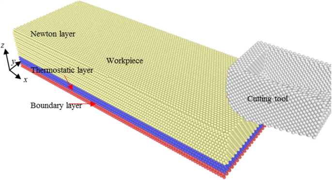
金刚石切割模型仿真模型
潜在功能
铜-金刚石切割系统主要涉及两种原子,即铜原子和金刚石原子。在MD模拟中,应准确描述原子间相互作用,以保证模拟结果的计算精度。因此,合理选择潜在功能至关重要。本研究采用常用的嵌入原子法(EAM)势函数来描述铜原子之间的原子间相互作用[21]。 Morse 函数用于计算铜原子和金刚石原子 (Cu-C) 之间的相互作用,主要取决于 r.
$$ E={D}_0\left[{e}^{-2\alpha \left(r-{r}_0\right)}-2{e}^{\alpha \left(r-{r} _0\right)}\right] $$ (1)其中 E 和 D 0 指对势能和内聚能,α 代表一个常数,r 0 是平衡距离,r 是两个原子之间的距离。对于 Cu-C 相互作用,D 0 是 0.087ev,r 0 为 0.205 nm [22],并且 α 是 51.40 nm −1 . 对于刀具(C-C)中碳原子之间的相互作用,金刚石原子之间明显强于铜原子的键强度可以忽略不计。分析时将刀具视为刚性刀具。
切割深度的定义
切削深度 (a )定义为工件表面最高点与刀具最低点之间的距离。工件原子的大小通常用原子半径(r w ). 如图 2 所示,当目标是从工件表面去除最上面的第一原子层时,理论上,所使用的最大切削深度可以如下获得:
$$ {a}_{\mathrm{max}}={r}_w+0.5\ast {d}_{layer} $$ (2)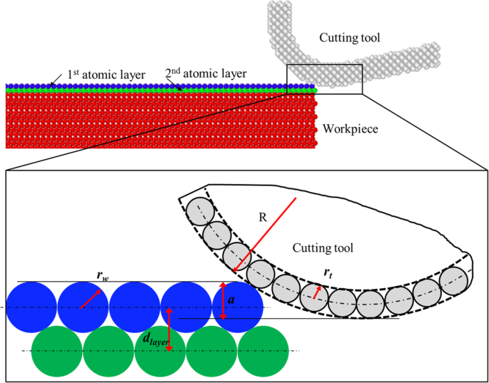
单原子层去除切割深度定义示意图
在这里,d 层表示工件表面上最顶层相邻原子层之间的间距。本研究中,所有分析均基于单晶铜工件的(111)面;因此,r w 在方程式中(2)指的是铜原子的半径,即1.28 Å。 d 层为 2.087 Å。当 a 大于 a 最大,刀具的最低点将与第二原子层直接接触,并可能引起材料变形甚至去除。因此,在本研究中,使用的切削深度小于 a 最大 (2.32 Å).
基于这些发现,在a比率的各种组合下,基于切割的基本单原子层去除机制将发生很大变化。 R 和 a r w .
结果与讨论
根据MD结果,原子尺寸效应和切削刃半径效应都极大地影响了基于切削的单原子层去除过程。在下面的部分中,为了清楚地描述原子尺寸效应和刀具边缘半径效应,切削深度的比率(a ) 到工件原子半径 (r w ), a/r w , 切削深度(a ) 到边缘半径 (R ), a/R , 受雇。从切屑形成、表面生成、次表面变形和原子位移行为等方面系统地研究了分析结果。研究结果为基于切割的单原子层去除机制的典型特征提供了详细的见解。
芯片形成
分析结果表明,由于工件原子尺寸效应[20],切削深度比(a)有两个临界值 ) 到工件原子半径 (r w ),即临界值1(C1)和临界值2(C2),将切屑形成行为分为不同情况。
- a.
a/r 的比率 w 小于临界值1(C1)。
图 3 显示了在切削深度约为 1.1 Å 时,在不同刀具刃口半径下的 MD 模拟结果。这里,切削深度的比值 (a ) 到工件原子半径 (r w ) 是 0.781。
<图片>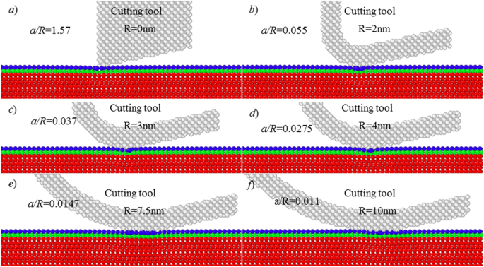
切削深度为 1.1 Å
时的模拟结果尽管增加了切削刃半径,但在加工过的每个 Cu(111)表面上都发生了弹性变形。在切削过程中没有切屑形成和材料去除。研究表明,切削深度应大于1.1 Å,才能去除Cu(111)表面的材料。
- b.
a/r 的比率 w 大于C1,但小于临界值2(C2)。
当切削深度大于约 1.1 Å 时,即 a/r w 大于 0.781,工件表面有材料去除。如图 4 所示,部分材料从工件表面去除,但最顶层第一层内的大量原子仍留在新处理的表面上,形成表面缺陷。此外,随着边缘半径增加到 7.5 nm,a/R 是 0.019。在这种情况下,第一原子层中的一部分原子被压入第二层甚至第三原子层,如图4e所示,这应该归因于刀具的挤压作用。这也表明刀具边缘半径效应开始对材料去除过程产生影响,尽管无法获得连续的材料去除。
- c.
a/r 的比率 w 大于C2。
切削深度为 1.4 Å
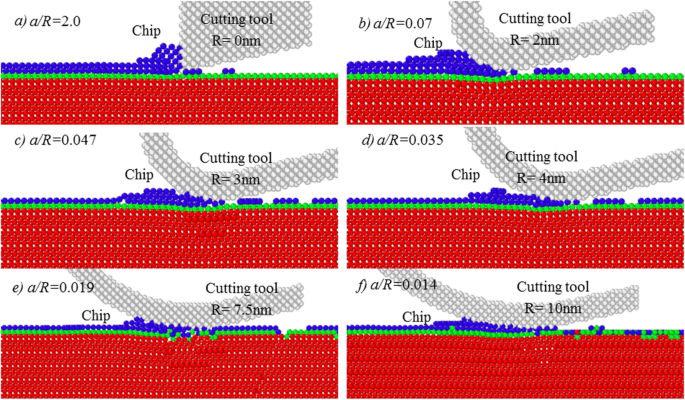
时的模拟结果图 5 显示了切削深度约为 2 Å 时的切屑形成。这里,a/r 的比率 w =2 Å/1.28 Å =1.563。与图 3 相比,随着切削深度增加到 2 Å,目标原子层内的原子可以通过芯片形成连续稳定地去除。这表明切割深度已经大于单晶铜的最小切屑厚度,最小切屑厚度可以下降到单原子层,切割深度约为2 Å。切割后,第一原子层内的材料从工件表面完全去除。
<图片>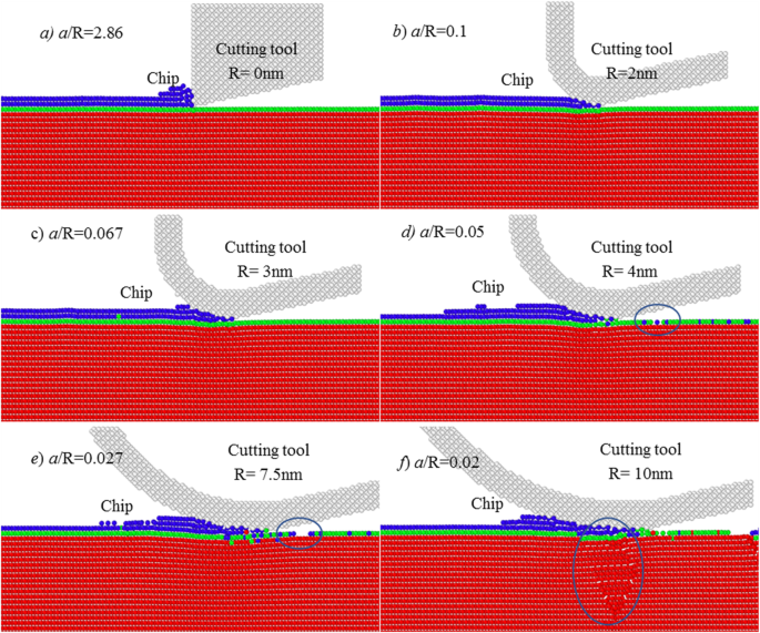
ACS 切削深度=2 Å
的仿真结果然而,在图 5 中也可以注意到,由于 a/R 的比值的增加 ,第一原子层中的原子经历了明显不同的去除过程,特别是加工表面的切割引起的变形。在切削深度为 2 Å 时,使用锋利的刀具时,即 a/R 为5.70,加工表面仅发生轻微变形。随着切削刃半径增加到 3 nm,a/R 为0.134,弹性变形幅度明显增大。
当刀具边缘半径增加到 4 nm 时,如图 5d 所示,目标第一原子层内的许多原子已被压入第二原子层,形成新的加工表面。在刀具边缘半径约 7.5 nm 处,第一层的部分原子甚至扩散到第三层原子。当刀刃半径达到10 nm左右时,发生明显的弹塑性变形,这也可以在下面的3.3节中确定。
因此,基于切割的单原子层去除不仅取决于a/r w ,还有 a/R 的比率 .为了实现机械切割的单原子层去除,即原子尺度的材料去除,应同时考虑原子尺寸效应和切削刃半径效应,与微/纳米切割和常规宏观切割有显着区别。
表面生成
基于切割的原子层去除的目的之一是获得具有理想晶体结构的无缺陷加工表面。最近研究了工件原子尺寸对 ACS 切割表面生成的影响 [20]。在本研究中,为了清楚地表明ACS切削中切削刃半径对表面生成的影响,对新加工表面的表面形貌和表面组成进行了如下研究。
地表地形
图 6 显示了加工后的 Cu(111)表面在不同边缘半径处的表面形貌。这里,采用 2 Å 的切割深度。如图 6a、b 所示,当刀具刃口半径小于 3 nm 时,可以获得具有理想晶体结构的 Cu(111)表面。至于工件表面左侧的缺陷,则是由于刀具切削退刀时的变形所致。在稳定阶段的切削过程中,加工表面没有形成表面缺陷。
<图片>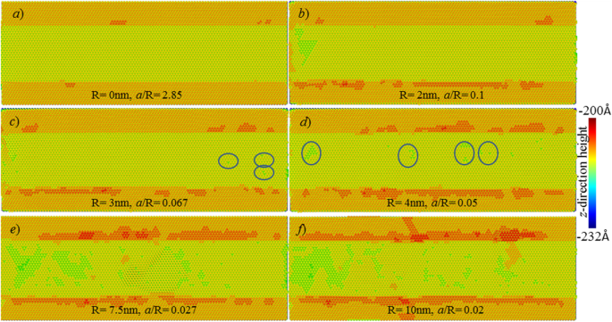
刀具边缘半径对表面形貌的影响。原子根据它们的 z 方向高度着色
然而,随着刀具刃口半径的增加,加工表面逐渐形成许多缺陷。在4 nm的边缘半径处,在加工表面上形成了许多凹坑状缺陷,见图6d。此外,当刀具刃口半径等于或大于5 nm时,会形成大量表面缺陷,严重降低表面质量。在这种情况下,已经从工件表面去除了一层以上的原子。因此,可以确定在2 Å的切削深度下,当刀具刃口半径小于3 nm时,可以在Cu(111)表面实现单原子层去除。由于切削刃半径效应,切削深度比(a ) 到边缘半径 (R ) 应大于一个阈值,以便通过基于切割的单原子层去除实现无缺陷的加工表面。这里,a/R 比值的临界值 是 [0.05, 0.067]。
表面构成
图 7 显示了在不同刀具边缘半径和 2 Å 切削深度下加工表面的组成。这里,绿色和蓝色原子是来自第一层和第二层的原子,而红色原子是位于第二层以下的原子。如图 7a 所示,当使用锋利的刀具时,a/R 的比率 为 2.85,加工表面仅由第一层原子组成。该结果表明目标第一原子层已从工件上彻底去除。而且,这意味着材料去除是以逐层的形式进行的,其中去除的材料仅来自工件表面的目标第一原子层。
<图片>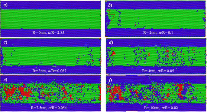
加工表面的表面组成。原子根据原子层数着色
然而,当刀具边缘半径为 2 nm 和 3 nm 时,如图 7b、c 所示,加工表面由两个原子层(蓝色和绿色)复合而成。这表明虽然已实现单原子层去除,但表面生成过程涉及最少 2 个原子层。此外,当刀具刃口半径大于4 nm时,加工表面第一层原子有大量的原子,说明第一层的许多原子已经被挤压形成新的表面。
因此,随着切削刃半径的增加,表面的生成发生了很大的变化。所涉及的两种表面生成机制总结如下:
- 1.
逐层 :目标第一原子层被完全去除以产生新的加工表面。切割过程中只去除第一层内的原子。
- 2.
多层去除 :虽然可以实现单原子层去除,但目标原子层内的原子会经历两种典型的位移行为。一部分原子在剪切应力驱动的位错运动中形成切屑,而其他原子则在刀具的作用下被挤压到加工表面。材料去除过程至少涉及两个原子层。
地下变形机制
在纳米切削中,切削过程中被加工表面会发生弹性变形和塑性变形。刀具越过工件表面后,弹性部分回弹,而塑性变形部分将导致持续变形[1, 2]。随着切削深度减小到原子尺度,在向单原子层去除的切削中,假定加工表面仅发生弹性变形。为了验证这一点,我们分析了切削过程中和切削后的工件亚表面变形状态。图 8 说明了工件表面下不同刀具边缘半径的缺陷结构。这里,原子根据中心对称参数(CSP)着色,CSP小于3的原子被省略,代表具有完美FCC结构的原子。
<图片>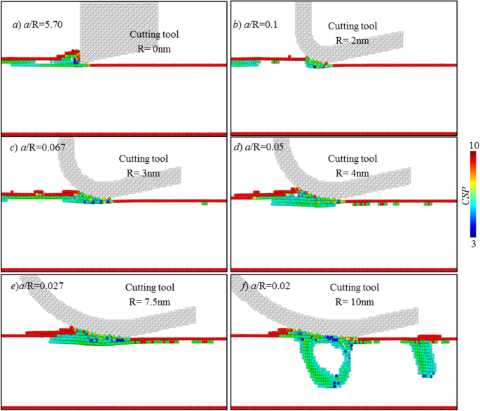
加工表面的表面组成。原子根据它们的 CSP 着色
当切削刃半径小于4 nm时,加工表面不会形成亚表面缺陷。切削加工时,加工面只有弹性变形。
如图 8 所示,当切削刃半径等于或大于 4 nm 时,存在初始化的亚表面缺陷。此外,随着切削刃半径的增加,次表面缺陷的数量显着增加。当边缘半径达到10 nm左右时,就形成了一个位错环,切割后不会消失,如图9e所示。它清楚地表明了加工表面发生的塑性变形。
<图片>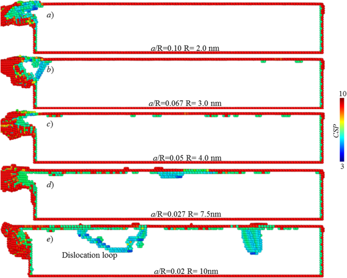
不同刀具边缘半径处的次表面缺陷。原子根据它们的 CSP 着色
刀具越过工件表面后,弹性变形部分会回弹;因此,部分次表面缺陷被消除。如图 9a-c 所示,最后,当刀具边缘半径为 2 nm 或 3 nm 时,不存在次表面缺陷。
对于塑性变形的部分,它会导致持久变形。如图 9 所示,当刀具边缘半径为 7.5 nm 时,残留的次表面缺陷数量很少。当刀具刃口半径为10 nm时,位错环和堆垛层错最终存在于工件亚表面。
由以上分析可以推断,要实现基于切削的单原子层去除,应避免塑性变形,只允许加工表面发生弹性变形。它被认为是基于切割的单原子层去除工艺的特征之一。
原子置换行为
根据 MD 轨迹文件,位错运动主导了基于切割的单原子层去除过程。图 10 显示了使用不同刀具边缘半径的模拟结果。在2 nm的边缘半径处,在刀具的作用下,只有第一个原子层沿切削方向滑动形成切屑,其他原子层保持不动。可视为一个刃位错的一个截面。
<图片>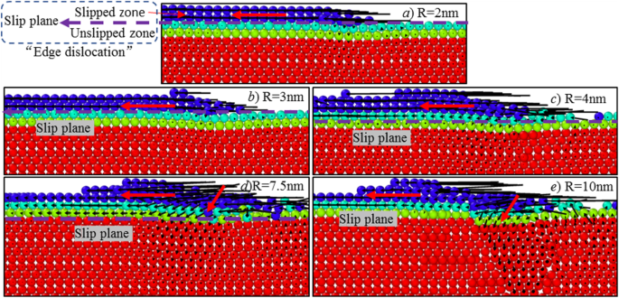
不同切削刃半径下的原子位移行为
随着刀具边缘半径的增加,第一原子层内的部分材料已被压入加工表面,导致第一层下方的原子层发生滑动。此外,随着刀具边缘半径的增加,经历材料滑移过程的原子层的数量趋于增加。当刀刃半径为 4 nm 时,除第一原子层外,第二原子层也沿切削方向进行材料滑移,如图 10 所示。当刀刃半径为 7.5 nm 时,随着刀具前进,最上面的三个工件表面的原子层沿切割方向滑动。此外,当刀具刃口半径增加到10 nm时,大量材料被压制形成新的加工表面;工件表面发生塑性变形(见图10e),如图9所示。
图 11 显示了目标原子层沿切割方向的滑移过程。滑移区的面积随着刀具的前进而不断扩大。在切割距离 17.5 nm 处,滑移区达到最大值。随后,滑移区内的材料不断形成切屑;芯片体积也增加了。
<图片>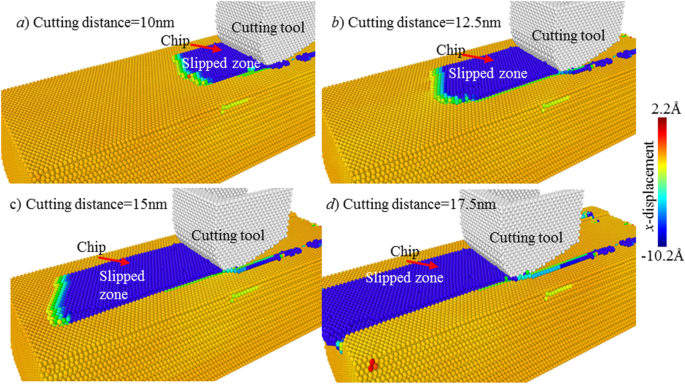
目标原子层在 2 nm 的切削刃半径处的滑移过程。原子根据它们的 x 方向原子位移值着色
总体而言,根据第 3.3 和 3.4 节中的分析,随着刀具边缘半径的增加,次表面变形机制和原子位移行为都发生了很大变化。在不同的刀具半径下,不同数量的原子层倾向于沿切削方向滑动,而加工表面会出现不同的变形机制,如表 2 所示。 此外,可以发现在基于切削的单原子层去除中过程中,切屑的形成受剪应力驱动的位错运动控制,与传统切割和纳米切割的切屑形成有显着差异,也可以看作是基于切割的单原子层去除的特征之一。
切削力
边缘半径效应的影响
图 12 显示了切削深度为 2 Å 时切削刃半径对平均切削力的影响。这里,切削力的切向分量和法向分量,即 F t 和 F n ,进行比较。如图所示,对于锋利的刀具,a/R 的比率 是 2.85,F t 16.4 nN 明显小于 F n 23.7 nN。随着刀具刃口半径的增加,F t 和 F n 增加。然而,F n 已表现出比 F 大得多的增长幅度 t .它清楚地表明,随着刀具边缘半径的增加,法向切削力对 ACS 切削过程中的材料去除过程的影响更大。然而,当刀具边缘半径大于约 3 nm 时,无法实现单原子层去除。因此,较大的法向切削力无助于实现基于切削的单原子层去除,宜采用较小的法向切削力。
<图片>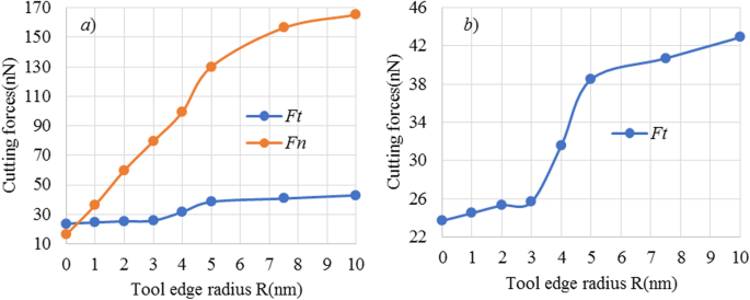
切削深度为 2 Å
时切削力与切削刃半径的关系图由于法向切削力提供压缩应力以在加工表面上实现弹性和/或塑性变形,切向切削力将为切屑形成提供剪切应力。因此,可以推断,基于切削的单原子层去除中的切屑形成应主要由切向切削力驱动。在图 12b 中还可以看出,F t 表现出三种变化,进一步导致不同的表面形貌(见图6),包括:
当刀具刃口半径小于约 3 nm 时,即 a/R 的比值 是 0.067,F t 大约保持不变,并且随着边缘半径的增加,它总是小于 25 nN。在这种情况下,仅从工件表面去除一个原子层。
当刀具刃口半径为 3 nm 和 5 nm 时,a/R 的比值 分别为 0.04 和 0.067,而 F t 明显增加到约 38.5 nN。因此,工件表面去除了一层以上的原子层,但形成的表面缺陷数量较少。
对于大于5 nm的边缘半径,F t 也逐渐收敛到一个恒定值。在这种情况下,去除了不止一个原子层。然而,在工件表面和亚表面形成了大量的表面缺陷。
可以得出结论,非常低的切向切削力可以在合理的切削刃半径(例如 2 nm)下实现基于切削的单原子层去除。反过来,尽管切向切削力较大,但无法实现单原子层去除。
原子尺寸效应的影响
图 13 进一步给出了切削刃半径为 2 nm 时切削力与切削深度的关系图。可以发现,在2 nm的切削刃半径处,随着切削深度的增加,法向切削力和切向切削力均呈现出三级变化。在大约 1.1 Å 和 1.6 Å 的切削深度处有明显的变化。对应的切削深度比(a ) 到工件原子半径 (r w ) 分别为 0.055 和 0.080,这是上述 a/r 的两个临界值 w 、C1 和 C2,如第 3.1 节所述。
<图片>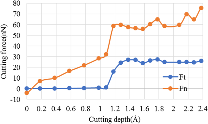
切削刃半径为 2 nm 时切削力与切削深度的关系图
When cutting depth is smaller than 1.1 Å, namely, the ratio of a/r w is less than 0.055, F t is always 0 nN, while F n is linearly increased to about 32 nN. However, the cutting forces could not enable plastic material deformation and removal on the workpiece surface. Consequently, there is only elastic deformation on workpiece surface, as shown in Fig. 3.
When the cutting depth is larger than 1.1 Å, but smaller than 1.6 Å, the ratio of a/r w is more than 0.055 but less than 0.080. If this case, F t has greatly increased from 0 nN to about 25 Nn, while F n further increased to about 58 nN. The cutting forces are larger enough to enable material removal on workpiece surface. At the cutting depth of 1.4 Å, there is chip formation and material removal on workpiece surface. But the stable and continuous material removal could not be realized and many defects are formed on the processed surface, as shown in Fig. 4.
When the cutting depth is larger than 1.6 Å, both F t 和 F n are large enough to enable continuous material removal on workpiece surface. Consequently, chip is stably formed over the workpiece surface, and the targeted atomic layer is continuously removed via chip formation, forming a new processed surface, as shown in Fig. 5b and Fig. 6b.
Overall, both cutting-edge radius effect and atomic sizing effect have an influence on cutting force in cutting-based single atomic layer removal process, thereby changing the material removal and surface generation process.
Discussions About Cutting-Based Single Atomic Layer Removal Mechanism
As per above analysis, both atomic sizing effect and cutting-edge radius effect have a great influence on the cutting-based single atomic layer removal mechanism. As summarized in Table 3, depending on the ratio of cutting depth to workpiece atomic radius(a/r w ) and the ratio of cutting depth to edge radius(a/R ), there are minimum 5 typical cases of material deformation and removal behaviours in cutting-based single atomic layer removal process. In this section, the fundamental material deformation and removal mechanism of each case is summarized.
In conventional machining, as cutting depth is significantly larger than the cutting-edge radius, the cutting-edge radius effect can be ignored. As the cutting depth is decreased to nanoscale, which is comparable or lower than the edge radius, the edge radius effect can be no longer ignored. In nanocutting, the material removal process is dominated by the extrusion deformation, which is greatly influenced by cutting-edge radius. As the cutting depth is further decreased to atomic scale, except for cutting-edge radius effect, a new sizing effect, atomic sizing effect [20] has a great influence on material removal.
As shown in Fig. 14, in the cutting-based single atomic layer removal process, there are two portions involving in cutting, i.e., nanometric cutting edge and the lowest cutting tool atoms (B )。 Such two portions could be coupled to enable single atomic layer removal. The size of cutting edge, regarded as ‘nano-tool,’ is described by edge radius (R )。 The cutting edge is the envelope curve of the outermost atoms in cutting tool. Regarding the lowest atoms, as ‘atomic-tool,’ it is described by workpiece atomic radius (r w )。 The cutting-based single atomic layer removal is the results of the coupled actions of nano-tool and atomic-tool on workpiece material.

Schematic diagram for cutting-based single atomic layer removal
Firstly, depending on the ratio of cutting depth (a ) to the workpiece atomic radius (r w ), i.e., a/r , there are three kinds of material deformation behaviour in ACS cutting process.
- 1.
The ratio of a/r w is smaller than critical value 1(C1).
As shown in Fig. 15, chip formation does not occur, but elastic deformation does occur on the workpiece surface. During cutting process, after workpiece passes the lowest point of cutting tool, the elastically deformed part would recover completely. Consequently, no material deformation and removal occurred on the topmost surface. In such case, the tool edge effect could be ignored. This ratio could be affected by material properties (case 1).
- 2.
The ratio of a/r w is larger than C 1 , but smaller than critical value 2 (C2).

Schematic illustration of cutting-based single atomic layer removal at the ratio of a/rw smaller than C1
As the ratio of the cutting depth to atomic radius (a/r w ) increases to be larger than C1 but smaller than critical value 2(C2), there is material removal on the workpiece surface, but it is noncontinuous. In such case, only part of material within targeted atomic layer is formed into chip by shear stress-driven dislocation motion, while others are remained on the workpiece surface. When cutting tool passes over the workpiece surface, the surface quality of the processed surface is seriously deteriorated (case 2) (Fig. 16).
- 3.
The ratio of a/r w is larger than critical value 2 (C2).

Schematic illustration of cutting-based single atomic layer removal at a/rw larger than C1 and smaller than C2
When the ratio of cutting depth to atomic radius (a/r w ) increases to be larger than critical value, there is a continuous material removal by chip formation during cutting process. In such case, the edge radius effects can no longer be ignored. For ACS cutting process, the maximum cutting depth is subnanometer order. At such extremely low cutting depth, regardless of the nominal rake angle, the effective rake angle is always largely negative. The negative rake face can produce the necessary shear stress to enable chip formation by dislocation motion and the compressive force to enable the elastic and/or plastic deformation on the processed surface.
Depending on the ratio of cutting depth (a ) to tool edge radius (R ), different kinds of elastic and/or plastic deformation process occur on the workpiece surface. There are two threshold values of a/R , namely, threshold value 1 (T 1 ) and threshold value 2 (T 2), leading to different material removal processes.
- a.
The ratio of a/R is larger than threshold (T 1 ).
As shown in Fig. 17, there is one atomic slip plane. The workpiece material below this plane would have an elastic deformation. As for the materials above this slip plane, it undergoes a plastic deformation by dislocation motion. A part of materials is also formed into chip by shearing stress-driven dislocation motion, while the other undergoes dislocation slip. After the workpiece passes the lowest point of the cutting tool, the elastically deformed part recovers completely (case 3).
- b.
The ratio of a/R is lower than threshold 1 (T 1), but larger than threshold 2 (T 2).

Schematic illustration of cutting-based single atomic layer removal at a/rw larger than C2 and a/R larger than T1
Under the action of cutting edge, minimum two atomic layers undergo dislocation slip, while elastic deformation occurs on the processed surface, as shown in Fig. 18. The cutting edge provides a force to generate the shear stress to enable chip formation by dislocation motion and compressive stress to induce elastic deformation on the processed surface. In such case, part of material within the targeted atomic layer is formed into chip by dislocation motion, while the other is extruded into other atomic layers to form new processed surface. It also drives the slip of other atomic layers on the workpiece surface, leading to the negative dislocation climb. After workpiece material passes the lowest point of the cutting tool, the elastic portion springs back (case 4).
- c.
The ratio of a/R is lower than threshold 2 (T 2).

Schematic illustration of cutting-based single atomic layer removal at a/rw larger than C2, a/R larger than T2, smaller than T1
As the ratio of a/R decreases to lower than T 2, there is either no chip formation or extremely small volume of chip formation, but elastic-plastic deformation occurs on the processed surface, as shown in Fig. 19. After workpiece material passes the lowest point of cutting edge, the elastic deformed part springs back. The plastic deformed part (Δ ) leads to lasting deformation. Such ratio is related with material properties, tool geometry and process conditions (case 5).

Schematic illustration of cutting-based single atomic layer removal at a/r larger than C2 and a/R lower than T2
结论
In the present study, both of atom sizing effect and cutting-edge radius effect are analysed to investigate their influence on chip formation, surface generation, subsurface deformation, and atomic displacement behaviour during the cutting of monocrystalline copper towards single atomic layer removal. The following conclusions can be drawn.
- 1.
A new model is proposed to describe the underlying material deformation and removal mechanism in the cutting-based single atomic layer removal process, which exhibits four characteristics, including chip formation by dislocation motion, elastic deformation occurring on the processed surface, atomic sizing effect, and cutting-edge radius effect.
- 2.
Both of atomic sizing effect and cutting-edge radius effect have a great influence on the material deformation and removal during the cutting process of monocrystalline copper towards single atomic layer removal. With a specific ratio of cutting depth to workpiece atom radius (a/r w ) and that of cutting depth to edge radius (a/R ), cutting-based single atomic layer removal could be achieved on Cu (111) surface.
- 3.
Chip formation is affected by the ratios of a/r w and a/R . There is a chip formation only when the ratio of a/r w is larger than one critical value (C1) and the ratio of a/R is smaller than one threshold value (T1). Moreover, chip formation is mainly dependent on the shear stress-driven dislocation motion, significantly different from the extrusion-dominated chip formation in nanocutting and shearing-dominated chip formation in conventional machining.
- 4.
Single atomic layer removal can be achieved via layer-by-layer removal and multi-layer removal. The former one refers to that the targeted atomic layer could be either fully removed from workpiece surface. The latter one means that the first atomic layer is partly removed while the remaining materials are pressed into other atomic layers, forming a new processed surface.
- 5.
There is only elastic deformation occurring on the processed surface during ACS cutting process, different from the elastic-plastic deformation in nanocutting. It can be regarded as one characteristic feature in ACS cutting.
- 6.
Depending on the combined effect of atom sizing effect and cutting-edge radius effect, there exist five cases of material deformation and removal processes during the cutting-based single atomic layer removal, i.e., no workpiece material is removed (case 1), workpiece materials are non-continuously removed (case 2), a part of materials is formed into chip while others undergoes material slip via dislocation motion (case 3), a part of materials within the targeted atomic layer is formed into chip while others are extruded into other atomic layers to form new processed surface (case 4), and the elastic deformed part springs back, while the plastic deformed part leads to a lasting deformation (case 5).
数据和材料的可用性
Authors declare that the materials, data, and associated protocols are available to the readers, and all the data used for the analysis are included in this article.
缩写
- ACS:
-
Atomic and close-to-atomic scale
- ACSM:
-
Atomic and close-to-atomic scale manufacturing
- MD:
-
分子动力学
纳米材料
- 用于 Micro-LED 和 VCSEL 的高级原子层沉积技术
- 协同光催化吸附去除 AgZnO/多金属氧酸盐纳米复合材料的基本洋红色效应
- 通过原子层沉积和水热生长制备的抗菌聚酰胺 6-ZnO 分层纳米纤维
- 通过等离子体增强原子层沉积制备的 Co3O4 涂层 TiO2 粉末的光催化性能
- 通过超循环原子层沉积调节 ZnO 薄膜的费米能级
- 用分子动力学研究冲击方向对磨料纳米切割过程的影响
- 在 c 面 GaN 上沉积的 AlN 原子层中界面和电特性的厚度依赖性
- 使用二氧化碳的低温等离子体增强原子层沉积 SiO2
- 具有通过原子层沉积制造的 Al2O3 钝化膜的硅纳米线异质结太阳能电池
- 通过原子层沉积制造的用于具有增强电容的超级电容器电极的 TiO2 纳米膜
- 通过原子层沉积制造的基于 Ru 的 RRAM 器件中的负差分电阻效应
- 单斜切与双斜切锯比较