

用分子动力学研究冲击方向对磨料纳米切割过程的影响
摘要
磨粒流抛光在现代超精密加工中占有重要地位。悬浮在磨料流介质中的超细颗粒以纳米级去除材料。在本文中,进行了三维分子动力学 (MD) 模拟,以研究在磨料流抛光过程中冲击方向对磨料切割过程的影响。利用分子动力学模拟软件Lampps模拟SiC磨粒在不同切削角度(0 o –45 o )。在摩擦系数不变的情况下,我们发现切削角和切削力之间存在直接关系,这最终会增加磨粒流加工过程中的错位数量。我们的理论研究表明,小切削角有利于提高工件表面质量和减少内部缺陷。但切削角与摩擦系数无明显关系。
背景
在现代超精密加工中,材料去除技术在微电子、微机械和光学元件制造中发挥着重要作用。对具有高尺寸精度和高质量表面的小型化设备的需求,使得超精密工艺成为上述领域的主要选择 [1]。此外,表面成分和亚表面结构的变化是在纳米长度尺度上的。磨粒流抛光技术在精密加工的许多领域中都发挥着重要作用,就像其他非传统的精加工技术一样,可以提高表面质量。由于其重要作用,这项技术吸引了许多研究人员。 E. Uhlmann 等研究人员报道了针对磨粒抛光陶瓷表面的计算机模拟设计实验,以验证各种加工因素对切削材料的影响的磨削液流量[2]。 Sehijpal Singh 和其他研究人员使用磨料流抛光技术切割铜和铝材料。通过扫描电子显微镜分析,他们发现了工件的深槽表面 [3]。 G. Venkatesh 等研究人员报道了圆锥齿轮在精加工复杂表面上的超声辅助磨粒抛光技术。在该技术中,磨粒速度高于常规磨粒流与工件表面碰撞,可提高加工效率。从他们的实验和理论方法中,他们发现该技术是齿轮叶片精加工的最佳选择之一 [4, 5]。 K. Kamal 等人。研究了磨料液在流体磨料粘度、剪切速率和蠕变时间等方面的流变特性[6]。然而,大多数磨粒流抛光研究都是基于宏观层面的,很少有人关注微观层面。在磨粒流抛光过程中,介质中的悬浮颗粒会随着微切削工件表面的冲击,以一定的速度沿介质流动(图1)。
<图片>
磨料切割工件草图。所有的数字都是关于冲击方向对磨料纳米切割过程的影响的分子动力学。图1为磨料切割工件示意图。在磨粒流抛光过程中,介质中的悬浮颗粒会随着微切割工件表面的冲击,以一定的速度沿介质流动
由于磨粒的形状不规则,具有一定的棱角,作用于工件表面,类似于刀具。但切割过程是在原子尺度上,这与材料去除过程明显不同。纳米级切割涉及的材料表面只有几纳米或更小,但很难通过实验观察到这一过程。因此,MD模拟作为一种理论研究方法在研究纳米切割过程中非常有用。分子动力学作为一种计算机模拟技术,它使用基于时间的统计力学方法来研究原子之间的相互关系以进行条件预测和分析。这也是模拟和理解材料去除过程的强大工具。在文献中,有许多研究将 MD 作为研究精密加工的工具。 Oluwajobi 和 Chen 在铜纳米加工的 MD 模拟方面做了大量工作 [7]。在他们的研究中,他们研究了纳米加工的各种参数,例如最小切割深度、几何形状和原子间势 [8]。此外,MD 模拟结果在过去也成功地解决了与硅等脆性材料的纳米切割过程有关的许多问题 [9]。科曼杜里等人。使用 Tersoff 电位对无缺陷的纯硅单晶进行了 MD 模拟。他们研究了前角、切削宽度、切削深度和后角对材料去除和表面生成的影响 [10]。戈尔等人。研究了纳米切割过程中碳化硅延性响应的原子方面。他们发现了 sp3-sp2 有序-无序转变的存在,最终导致了金刚石的石墨化 [11]。蔡等人。使用 MD 研究了硅的纳米级延性模式切割。他们报告了刀具切削刃及其对工件材料中剪切应力的影响 [12]。阿拉芬等人。已经讨论了切削刃半径在硅晶片的纳米级延性模式切削中的影响 [13]。其他各种研究人员也强调了使用 MD 模拟对硅进行纳米加工的不同条件。研究包括切削力、切削深度、温度、剪切应力和其他参数。然而,在这方面缺乏足够的实验验证。方启红等。研究了不同尺度不同异质材料中位错的相互作用机制,以及位错与材料韧性与断裂损伤的关系。他们使用分子动力学模拟来研究三种不同晶体结构上的纳米压痕,包括单晶、多晶和纳米孪晶多晶铜。随着划伤速率的增加,由于塑性变形剧烈和切屑体积大,划伤力和工件温度不断升高,导致位错滑移、GB滑移和孪生/去孪生[14, 15]。
方法/实验
在磨粒流抛光实验中,工件通常用碳化硅磨料进行切割。碳化硅磨粒模型建立后,利用Lammps软件对工件进行分子动力学模拟。构建了两种不同角度的碳化硅磨料切割单晶铜的模型。 SiC磨粒碰撞切割单晶铜仿真模型如图2所示。
<图片>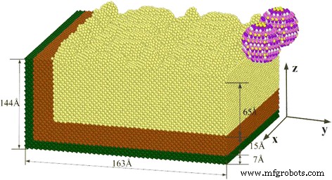
SiC磨料切割单晶铜仿真模型。图2为碳化硅磨料切割单晶铜仿真模型;我们制造了两个用于切割单晶铜的 SiC 磨料。在磨粒流抛光实验中,工件通常用碳化硅磨料进行切割。 SiC磨料模型构建完成后,对工件进行分子动力学模拟。构建了两种不同角度的SiC磨料切割单晶铜的模型
模型的大小如图 2 所示,模拟原子数为 159,020。磨粒半径为15 Å,磨粒中C原子和Si原子总数为1406个,碳原子数和硅原子数分别为681个和725个。模拟平衡系综的松弛步数设置为10,000步,碰撞模拟步数设置为100,000切割步,每步模拟为0.001 ps,切割模拟中,SiC磨粒在切割方向上的速度为80 m/s。 AFM分析值颗粒在抛光过程中碰撞微加工工件,SiC磨粒探索不同角度切削过程中的分子碰撞动力学。在磨粒流切削过程中,切削力随着切削速度的增加而增大,切削力的大小直接影响切削效果。因此,选择合理的切割速度对切割质量有着重要的影响。为了实现高质量的切割,我们选择了80 m/s的切割速度,因为它产生的切割力可以迅速破坏工件原子之间的相互作用[16]。
在低切削速度(如 10 m/s)的分子动力学模拟中,原子位移图以及碳化硅磨粒的切削力和切削角度如何随模拟步长变化的模式,如图 1 和图 4 所示。 3、4,由于切削速度太小,切削力也不足,导致晶格变形和错位少得多。整体而言,切割效率低,切割质量相对较差。相比之下,当显微实验切割速度达到80 m/s时,铜原子之间的化学键可以快速有效地断裂,从而达到即时高质量切割的目标。因此,综合分析,80 m/s的切削速度对仿真来说是合理的。
<图片>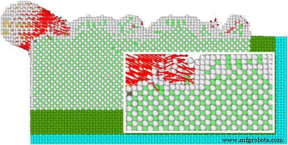
低速原子位移
<图片>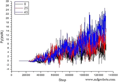
切削力、切削角度与仿真步长的关系
为了模拟可行性和可信度,我们选择了一个合理的经验势函数来考虑原子的原子间势。根据对象的不同,我们可以将势函数分为对势函数和多体势函数。单晶铜和磨粒之间的两个模型用莫尔斯电势描述它们之间原子的原子间势[17],EAM势用于描述铜原子之间原子的原子间势[18,19,20],碳化硅颗粒之间的相互作用使用 Tersoff 电位来描述 [21]。
在抛光过程中,磨粒在介质中的碰撞方向是随机的;它们的轨迹并不完全沿着工件表面。在微切削过程中,磨粒的切削方向并不总是与工件材料正交。切削角是指磨粒切削方向与水平面夹角的度数。当颗粒接近工件表面时为正。切削角示意图如图5所示。
<图片>
切角示意图。图5为磨粒切割时不同切割角度示意图。不同方向的磨粒切割工件材料,材料会有不同的性能和加工质量
在这项研究中,MD 模拟被用来模拟具有不同冲击方向的切割单晶铜的多磨料。如图5所示,在铜工件表面粗糙的情况下,切割角度在0°到45°之间。
结果与讨论
碳化硅磨料切削力学碰撞分析
碳化硅磨料对单晶铜材料切割的影响是通过破坏铜材料单晶的晶格结构来实现的。在击穿过程中,铜原子之间的相互作用,SiC 磨粒的 C、Si 原子对工件材料的 Cu 原子施加的剪切应力被确定为切削力,这是切削力的重要物理参数深刻反映了单晶铜工件材料的去除过程。如前所述,微观和宏观切削力之间存在很大差异。一般情况下,宏观切削力是切削力和磨削力的总和,而微观切削中,切削力是由磨粒与工件原子之间的相互作用产生的。
在图6中,我们展示了磨粒在不同方向的剪切应力的变化、不同方向剪切应力的影响以及切削力沿不同切削角度的分布。
<图片>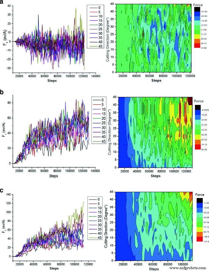
切削角度和模拟步长如何影响切削力。图6为碳化硅磨料切削力与切削角度及模拟步长图,随着切削深度的增加,破坏的晶体结构数量增加,切削力波动的最大值也变大。 一 [100] 方向的切削力。 b [010] 切削力的方向。 c [001] 切削力方向
碳化硅磨粒在[010]、[100]等不同角度的边缘切割冲击单晶铜材料。沿[001]和[010]方向的切削力为剪切力。在进一步的模拟中,切削深度逐渐增加,这使得沿 [001] 和 [010] 方向的切削力持续增加。然而,在一定限度内,这些力会发生波动,如图 6 所示。当磨粒向工件材料移动时,它完全改变了最外层铜原子与原子之间的相互作用(从吸引到排斥)碳化硅(Si 和 C)。最初,在磨削工件材料时,由于铜原子排斥力的存在,切削力不足。在精加工过程中,切削力应足够大,使磨粒容易断裂铜原子中的化学键而自由移动。此外,切削深度增量与原子相互作用有直接关系。当原子开始堆积时,切削力不断增加,直到磨粒进入工件,这需要一个稳态切削力。在这个相对稳定的阶段,切削力波动受到晶格变形程度、晶格重构、非晶相变和切屑产生的影响。随着磨粒沿切削方向前进,FCC晶格中的铜原子受到外力作用,导致铜原子发生位移。这种位移使 FCC 晶格坍塌,并将其转变为具有位错的新晶格结构。在切削力中也观察到类似的情况。沿[010]方向的切削力与粒子碰撞角不存在线性正相关关系。在0°、5°、10°及以上的碰撞中,[010]方向的力比其他切割方向的力更小,波动更小。以较小的角度切割,基本上去除毛刺,因为毛刺可以定义在 3.5 ~ 15 Å 的高度范围内。将这些方向相互比较,如果切削深度相对较小,则晶体结构的损伤和变形适中。因此,在整个切割过程中,沿[010]方向的剪切力保持较小,如图6b的曲线图所示。在模拟后期,切削力达到最小0°。还发现切割力与角度有直接关系,如图 6c 所示,这可以归因于当粒子速度达到 80 m/s 时,实现了更大的切割角度。另一方面,在相同的模拟步骤中,沿[001]方向的元件速度越大,角度越大,切割的粒子越深,原子晶格被破坏的越多。然而,切削角度和切削力之间存在正相关关系。当晶粒沿 [100] 方向移动时,C、Si 和 Cu 原子之间的摩擦是切削力的来源。因此,切削力并没有呈现出逐渐增加的趋势。然而,在进一步的模拟中,切削力增加和波动,这与晶格的变形和重建以及非晶结构相变的产生密切相关。在磨粒破坏之前,实现工件原子之间的相互作用以去除材料,最终使切削力持续增加。在增加磨料切削力时,超过临界值(原子结合力),原子晶格受损,键解离,导致无定形结构。实现这一点后,切削力下降到相对较低的值。在磨粒流加工的整个过程中,切削力波动不断出现,这是由于切削深度的增加,发生了更多的晶体结构破坏。因此,可以得出结论,在此阶段,切削力波动的最大值较大。如图 6b 所示,红色区域在模拟后期占据了更大的面积,这表明切削力显着提高。在相同的模拟时间下,切割角度小于15°时切割力较小,这意味着小部分晶格被破坏。
碳化硅磨料冲击切割过程的能量分析
热力学总能是系统中总势能和总动能的总和,它揭示了磨粒对工件做功的影响。切割角度对碳化硅磨料的影响对系统能量变化的影响如图7所示。 在切割单晶铜工件材料与碳化硅磨粒的过程中,磨粒对工件材料所做的功作用两种方式;一部分转化为动能,增加单晶铜原子与具有抛光作用的碳化硅颗粒接触的热量,另一部分转化为势能,使单晶铜工件的内部结构发生变化,晶格变形和晶格能量释放。
<图片>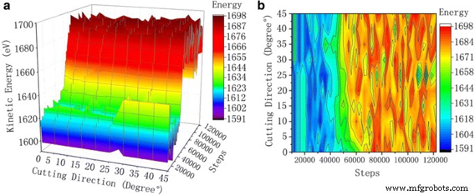
工件原子的动能曲线。图7为切割过程中不同切割角度的动能曲线。随着模拟步数的增加,原子的动能在较低的范围内波动,然后在波动范围内达到较高的范围。 一 3D 曲线。 b 轮廓
在单晶铜工件磨粒切削过程中,系统的动能与碳化硅磨料对工件材料所做的功密切相关。通过计算系统中粒子在每一时刻的速度,可以计算出系统的总动能:
$$ K=\sum \limits_{i=1}^N\frac{1}{2}{m}_i\left({v}_{\mathrm{ix}}^2+{v}_{\ mathrm{iy}}^2+{v}_{\mathrm{iz}}^2\right) $$ (1)式中,\( {v}_{\mathrm{ix}}^2 \), \( {v}_{\mathrm{iy}}^2 \), and \( {v}_{\mathrm {iz}}^2 \) 代表速度分量 x , y , z 方向原子,分别。
图 7 中的动力学曲线使我们得出结论,随着模拟步骤的增加,原子的动能最初在低范围内波动,然后进入更高范围。随着磨粒的运动,在最外层的铜原子和硅、碳原子(SiC)之间发现了长程排斥相互作用。工件中的铜原子开始获得动能并运动。当碳化硅颗粒接触铜单晶时,接触区域的原子温度升高,从而增加原子热运动。当切割稳定时,材料中铜原子的动能以动态平衡的方式传递和转化,原子的动能在较大范围内波动。
对动能的分析使我们得出结论,在切削过程中,当颗粒开始接触工件时,挤压区的原子发生晶格变形,原子坐标发生变化,位移随动能发生变化。随着磨粒进入单晶铜,当工件完全进入工件时,单晶铜工件的动能峰值出现。因为磨粒的动能和势能只是相互转化。但是,除了进入工件的运动粒子外,整个系统的能量不会改变。此外,碳化硅粒子的运动迫使工件原子与它们同时运动。原子摩擦产生的热量由位错运动释放的动能和应变能释放。
热能与动能的换算由下式计算:
$$ \frac{1}{2}{\sum}_i{m}_i{v}_i^2=\frac{3}{2}{nk}_B{T}_i $$ (2)在公式中,n 是原子数; vi 代表瞬时速度; k B 是玻尔兹曼常数,T 我 是原子的温度。
切削力会增加磨料与工件材料接触区域的原子温度。考虑到原子的热运动和原子的动能,铜原子的动能部分增加。模拟系统设置为规范系综;整个系统温度在一定范围内波动。磨粒切割过程中产生的热量迅速传递到恒温原子层,因此系统整体动能变化很小。
从图8的势能曲线可以看出,随着模拟步数的增加,工件中铜原子单晶间的势能也有增加的趋势。当碳化硅磨料与铜工件单晶接触时,从开始到完全稳定切割,工件材料逐渐变形,铜原子发生位移,导致晶体中晶格畸变。这也会导致弹性应力场,其中应变能增加。当应变能不足以重新排列材料原子时,就会发生原子错位,从而增加系统的总能量。对比 0° 到 45° 的电位曲线,我们可以看到原子在恒温下的热运动的一致性。碳化硅磨粒的原子动能与切削角之间没有显着关系。原子的动能与原子的热运动密切相关。但势能和总能量的变化明显与SiC磨粒的切削角有关。原子势能的大小随着切割角的增加而增加。当切割角在0°和20°之间时,观察到势能的明显变化。但是,当切割角在25°和45°之间时,势能保持不变,整体势能曲线从0°到20°切割角。如图 9 所示,总能量趋势与势能曲线相似。所有切割角度的总能量值彼此非常接近。这是因为在切割过程中,总能量等于系统的势能和动能,而动能并不随着切割角度的变化而变化。不同的切削角度工件的动能变化很小。因此,势能的变化曲线类似于总能量的变化曲线。对比图 9 的原子位移图可以发现,在相同的切削条件下,单晶铜工件的切削深度在切削角度在 25°~45°之间时更大,这可以归因于位移的增加铜原子。沿着SiC颗粒的[001]方向,会产生更多的晶格损伤和位错原子。在此期间产生的应变能较高,导致工件原子的势能变化曲线和总能量变化曲线较高。
<图片>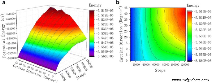
工件的势能曲线。图8为切割过程中不同切割角度的势能变化曲线图。随着模拟步数的增加,单晶铜原子表现工件之间的电位趋于增加。 一 3D 曲线。 b 轮廓
<图片>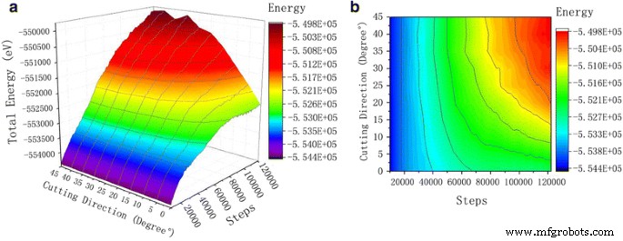
总能量曲线。图 9 显示了总能量曲线。 SiC在切割单晶铜工件的过程中,磨粒对工件的作用表现为两种形式:一部分转化为动能,原子热增加,抛光时局部动能变大单晶铜工件与碳化硅颗粒的接合面积;另一部分转化为势能,使单晶铜工件的内部结构发生变化,晶格变形,释放出晶格能并转化为势能。 一 3D 曲线。 b 轮廓
碳化硅磨粒碰撞切割过程中原子位移分析
在不同角度切割工件材料的过程中,磨粒沿切割方向运动,迫使工件中的铜原子运动。从工件的运动方向分析,磨粒对工件材料的影响、切屑的形成方式、材料的去除等,都一目了然。根据Ackland-Jones提出的键角分析方法,不同的原子晶格结构用不同的颜色标记,以供观察和分析。选取ZOY平面观察单个SiC颗粒的切割过程,放大切割区域的原子位移图,如图10所示。
<图片>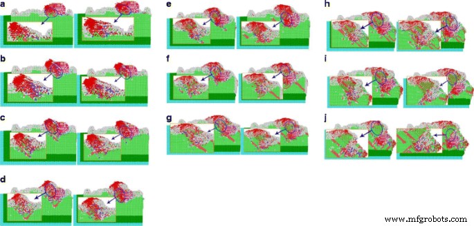
不同的切割角度会导致原子位移。图 10 描述了不同切割角度的原子位移。当单晶SiC磨粒与不同方向切割铜的工件碰撞时,随着SiC磨粒被切割,切割深度增加,由于切割方向的速度为80m/s,[001]方向的移动速度是 v z =0.8 ∗ sin θ ,随着切削深度的增加,切削角度的增加,[001]在相同的切削角度下模拟步长增加,同时切削深度变大。 一 0°位移。 b 5° 位移。 c 10°位移。 d 15°位移。 e 20°位移。 f 25°位移。 g 30°位移。 h 35°位移。 我 40°位移。 j 45°位移。 (原子色:  HCP结构,
  BCC 结构,
  FCC 配置为白色无定形结构)
当单晶碳化硅磨粒与不同方向切割铜的工件碰撞时,切割深度随过程增加。切割方向的速度为80 m/s,其中[001]方向的分量速度为v z =0.8 ∗ sin θ . At the same simulation step, cutting depth increases with increasing the cutting angle. As shown in Fig. 10, there is an atomic position shift in both of the surface and interior of the workpiece material, contacting with the abrasive grains, where atoms of different lattice types are arranged and doped with each other. Due to the movement of these abrasive particles, the copper atoms accumulated at the tip of the abrasive grains, which results no cracks during abrasive particles cutting. It can be seen that the material removal mode of the abrasive particles is plastic deformation. At the same time, due to abrasive cutting, the atoms displacement in single crystal copper increases from 15° to 45°.
The number of the workpiece atoms along the abrasive grain motion direction also increases, and the atomic displacement is perpendicular to the direction of abrasive cutting. This part of the atomic displacement is due to that of the abrasive particles, change the cutting action to the extrusion upon the workpiece atoms. At cutting angle, the abrasive particles is between 0° and 10°, while the cutting depth is smaller than those of the 15° to 45°. Abrasive particles are performing mainly the cutting function, the extrusion of the workpiece atoms is marginal, and the number of atoms is small whose displacement direction is perpendicular to the direction of the abrasive grain motion. With the repeated cutting on the workpiece surface by numerous abrasive particles, the abrasive particles having large cutting angle produce deep pits on the workpiece material during the whole cutting process, while ones following smaller cutting angles will continue cutting along the cutting mark produced by the former. Under the combined action, the workpiece material is cut to a certain depth (micro-cutting) followed by whole abrasive flow polishing.
Dislocation Collision Analysis for SiC Abrasive Cutting
Dislocation is a special arrangement of atoms in crystal along certain crystal surface and crystal direction, or a boundary between the slip zone and the non-slip zone on the slip surface. Dislocation can be divided into edge dislocation, spiral dislocation, and mixed dislocation, among which mixed dislocation is most common. In the process of abrasive particle cutting, the single crystal copper workpiece is plastically deformed, the atoms move, and the crystal lattice breaks and reconstructs, which results in a large number of dislocations. The analysis for dislocation and bond angles at different incidence angles is shown in Fig. 10. In the simulation model of abrasive flow simulation, two abrasive particles are used for cutting the workpiece material. For ease of analysis, the generation and change of different dislocation lines in single crystal copper material, during cutting process and the different lattice structures in the cutting part are analyzed in the view of one single SiC particle on the YOZ surface, as shown in Fig. 11.

Different angles-bond angle dislocation line charts. Figure 11 represents the cutting dislocation line and the bond angle. As the repeated cuttings on the workpiece surface are done by the numerous abrasive particles during the polishing process, in the entire cutting process, the abrasive particles with larger cutting angle produce bigger pits, while the following abrasive particles with smaller cutting angles continue to polish along the cutting trace. Therefore, certain depth is done on the workpiece material and the whole micro-cutting of abrasive flow polishing is achieved. 一 Dislocation lines with 0° cutting angles. b Dislocation lines with 5° cutting angles. c Dislocation lines with 10° cutting angles. d Dislocation lines with 15° cutting angles. e Dislocation lines with 20° cutting angles. f Dislocation lines with 25° cutting angles. g Dislocation lines with 30° cutting angles. h Dislocation lines with 35° cutting angles. 我 Dislocation lines with 40° cutting angles. j Dislocation lines with 45° cutting angles. (Note:the upper part of the key angle analysis, the figure in the atomic color: HCP
HCP  BCC
BCC  Amorphous structure
  Abrasive grain; the lower part of the dislocation line diagram, the figure dislocation line color:
 Stair-rod,
  Shockley,
  Hirth,
  Perect,
  Frank,
  Burgers vectors)
Key angle analysis diagram of each cutting angle is shown in Fig. 11, where the sample from the interior workpiece simulation at time 60 and 70 ps, the atoms are colored individually according to different arrangement of atoms through BAD technology. To facilitate the analysis of the lattice changes in the cutting part, atoms of the FCC structure in the workpiece material are removed. By DXA techniques, different types of dislocations are marked in diverse colors:red arrow indicates the Burgers vector (Burgers vectors), green for Shockley partial dislocations (Shockley), light blue for the Frank partial dislocations (Frank), pink pole position for the pressure error (Stair-rod), and blue for the whole dislocation (Perfect).
As can be observed from the analysis of the bond angle portion in Fig. 11, a large number of dislocations and lattice deformations occurred under the impact of external cutting forces. The bond angle analysis shows that the internal HCP structure of the workpiece appears more clearly with increasing of cutting angle. On further simulations, the structure of HCP increases gradually. The silicon carbide particles continuously cut and squeeze the workpiece material at 80 m/s speed, resulting in a phase transition from the FCC structure to the HCP structure. During this phase transition, the atomic strain of the workpiece continues to increase. However, when the stress state of atoms of the workpiece has exceeded the threshold of thermodynamic phase transition, it turns to metastable state. As the strain increases, the HCP phase begins to nucleate and grow spontaneously, and the FCC lattice of copper undergoes absolute destabilization, which induces a sudden change in mechanical quantities. As the kinetic energy of the atom is directly related to the atomic temperature (formula 1), there is a saltatory augment in the kinetic energy change curve, as can be seen from Fig. 7. This is due to high strain energy, accumulated in the single crystal copper workpiece before the nucleation of HCP. The HCP structure increases the system temperature through metastable nucleation and partial stress release. Due to the abrasive cutting and extrusion, bonds of copper atoms in workpiece material break down which results in disorder. The original regular lattice structure is broken, where the partial copper atoms gradually change into disorder and form an amorphous structure. It can be seen from the bond angle analysis diagram that (Fig. 11) atoms with relatively disordered displacement tend to form amorphous structures at 60 and 70 ps, which is because of silicon carbide abrasive particles. At the same time, many atoms with the same displacement direction are transformed into HCP structures. Meanwhile, the particles shear downward and the atomic structure is rearranged due to the displacement of atoms in the original amorphous structure, results an amorphous structure of HCP. Atoms that have already been transformed into HCP structures, even before the next cut stage, change back into amorphous structure. As the cutting depth increases, the number of amorphous atoms near the abrasive particles also increases.
When the FCC crystal structure undergoes cutting by abrasive particles, a shear stress generates in atoms, which results in the displacement of atoms in the lattice and the arrangement of various lattice structures. In moving the atoms of workpiece, the rigid displacements of the atoms produce dislocations, also called as dislocation lines (Fig. 11). Dislocation line can be termed as the boundary between the slip zone and the non-slip zone, on the slip surface. According to the relation between the dislocation and the PATS vector, dislocation is parallel to the PATS vector, called the screw dislocations. The vertical ones are edge dislocations, and the mixed dislocations are neither parallel nor vertical. In Fig. 11, most of the dislocation lines are neither parallel nor vertical to PATS vectors, which are typical mixed dislocations. In the cutting process of abrasive particles, the dislocation line changes, moves and grows around the abrasive particles. The closer the particle, the greater the density of the dislocation line. Dislocation lines are also very dense, when the arrangement of atoms is complicated. The abrasive particles marked as orange, produce a large amount of HCP, BCC, and amorphous structures around them, which interlace and blend with each other to form dislocations that increases the internal energy of the crystals. When atoms arrange their self just like shown in Fig. 12b, possess maximum potential energy. While for the arrangement, shown in Fig. 12a–b, the atoms situate at the lowest potential energy position. The number of dislocation lines is directly related to the magnitude of strain energy of the crystal. The total strain energy of the unit length dislocation can be measured with the given formula:
$$ W=\alpha {Gb}^2 $$ (3)
Schematic view of dislocation changes. Dislocation is a special arrangement of atoms in crystals. It is the crystal in the atomic arrangement along a certain crystal face and crystal orientation occurred in a certain wrong line, and it is the boundary of the slip surface within the area where the slip has occurred and the area with no slip has occurred. In Fig. 12a –c , the relative displacement of the rigidity of the upper atom and the underlying atom produce dislocations, the upper atom belongs to the sliding region, and the lower atoms belong to the non-slip region, they are in the slip surface of the intersection line which is called dislocation line, that is, dislocation. Figure 12 is the process of dislocation generation and development
Where, α is the geometric factor (type dislocations, dislocation density) parameter related to, and generally 0.5 ~ 1.0; G is the shear modulus, and b is the slippage distance.
When the workpiece material is being cut, particles break the atomic arrangement and the lattice reconstructs, which constitutes, macroscopically, the plastic deformation of the workpiece material. In the process of plastic deformation, the dislocation was supposed to escape from the crystal and decrease the dislocation density. However, this dislocation density increases due to dislocation propagation. There are many ways of dislocation multiplication and the main one is the Frank–Reed dislocation source theory, of which the growth mechanism is shown in Fig. 11. As illustrated in Fig. 11, the density of the dislocation line increases markedly from 60 to 70 ps when the cutting simulation proceeds, change both the number and shape of dislocation lines in accordance with Frank–Reed dislocation source theory. At simulation time of 60 ps, there are many long Shockley dislocations. But after another 10 ps simulating, the long Shockley dislocation line becomes less and shorter. The original straight dislocation lines turn into bent, which is especially evident near the abrasive grains. From formula 3, the strain energy of the dislocation is proportional to b 2 . From the viewpoint of energy, the dislocations with the smallest b in the crystal should be most stable with low energy; however, dislocations with larger b will break down into ones. In addition, the energy of the dislocation is valued by the unit length of the dislocation line. Given the shortest line between two points is the straight, the strain energy of straight dislocation is lower than that of the bent one, means straight dislocations are more stable. Frank–Reed dislocation source theory argued that the long dislocation line becomes shorter and breaks down into smaller dislocations, thus decreasing the strain energy of the crystal.
Analysis for Friction Coefficient Between Workpiece Surface and Abrasive Particles
To quantitatively disclose mechanical properties and surface effect of SiC abrasive cutting single crystal copper material, the tangential force ([010] direction) and normal force ([001]direction) on the cutting surface are further analyzed. The friction coefficient can be defined as the ratio of the tangential force to the normal force, with the formula below:
$$ f=\frac{F_y}{F_z} $$ (4)Figure 13 shows the variation of friction coefficient along different cutting angles during abrasive cutting. The change of friction coefficient can be divided into two periods. Period I, when the cutting distance is less than half of the size of the abrasive particle, the friction coefficient fluctuates violently in certain range due to surface effect of the material; while in period II, all the friction coefficients fluctuate in very small range, and the friction coefficients remains steady state at different angles. However, at cutting angle of 5°, there is a small amount of abnormal fluctuation at the end of simulation. Moreover, in period I, abrasive particles contact the workpiece atoms to the abrasive grains enter into the workpiece of half abrasive diameter (shown in Fig. 13b), the cutting movement distance reaches 7.5 Å. In Fig. 6, the cutting force change curve shows that the tangential force and normal force are in an oscillating phase during period I. Since the friction coefficient can be characterized as the adhesion among atoms in the contact surface and is related to the two atoms contacting with each other, regardless of the cutting mode, which can interpret the phenomenon that change of cutting angle does not cause significant change of friction coefficient, as shown in Fig. 13a.

Friction coefficients of different cutting angles. Figure 13 is the changes of the frictional coefficients during SIC particles cutting single crystal copper from different angles. The change in cutting angle did not cause significant changes in friction coefficient. It described two kinds of coefficient of friction in contact with the relevant atoms in the cutting process, regardless of the cutting mode. 一 Friction coefficient variation curve with cutting angle. b Instantaneous structure when SiC abrasive grains move 7.5 Å
结论
The micro cutting simulation of single crystal copper by SiC abrasive particles is achieved during abrasive flow polishing. Comprehensive analysis of the SiC abrasive cutting reveals that when SiC abrasive particles cut at angle from 0° to 15°, cutting forces in along Y and Z direction are relatively small and tend to stay steady. A larger cutting angle results more dislocations, which brings about larger grooves damaging of the workpiece material. In the process of cutting, it is necessary to avoid more dislocations, which has an immediate adverse effect on the performance of all aspects of crystal material. Therefore, a cutting angle of 0° is better than other angles. Considering the amount of dislocation produced, or the change of cutting force and energy in the cutting process; cutting with small or medium angles is not only beneficial for improving surface quality but reduce the internal defects.
纳米材料