

作为新型可调二元超晶格的双门纳米螺旋
摘要
我们从理论上研究了电子被限制在两个平行门之间的纳米螺旋中的问题,这些门被建模为带电导线。双门控纳米螺旋系统是一种二元超晶格,具有对栅极电压高度敏感的特性。特别是,能带结构对于某些栅极电压组合表现出能带交叉,这可能导致类准相对论狄拉克现象。我们对线偏振光和圆偏振光引起的光学跃迁的分析表明,双门控纳米螺旋可用于多种光电应用。
介绍
从第一作者在童年时期热情收集的螺旋形腹足动物化石,到无疑曾经定义了这些史前生物的 DNA 缠绕结构,螺旋几何在自然界中普遍存在 [1]。受自然发生的生物分子形状的复杂功能的启发 [2-6],预计其他具有适用于纳米技术的螺旋几何形状的系统将产生丰富的物理学并有助于新的应用。在过去的三十年中,纳米制造技术的显着进步导致在许多不同系统中实现纳米螺旋,包括 InGaAs/GaAs [7]、Si/SiGe [8]、ZnO [9-11]、CdS [ 12]、SiO2/SiC [13, 14] 和纯碳 [15-20],以及 II-VI 和 III-V 半导体 [21](有关当前技术水平,请参见参考文献 [21-26] ])。因此,预计在此类结构中会出现大量现象,从奇异的传输特性,如拓扑量子化电荷泵 [27, 28]、超导性 [29] 和自旋滤波 [30-32],到分子和纳米机械可拉伸电子学 [33, 34] 由于压电效应 [35]、传感应用 [36, 37]、能量 [38] 和储氢 [39] 以及场效应晶体管 [40, 41]。
基于纳米螺旋的设备的魅力最终源于螺旋结构拓扑中编码的固有周期性。特别是,使纳米螺旋受到横向电场(垂直于螺旋轴)会产生超晶格行为,例如超周期势上电子的布拉格散射,导致在超晶格布里渊区边缘的能量分裂通过电场线性可调的最低状态 [42, 43]。这种行为可能会导致布洛赫振荡和负微分电导 [44, 45],并且可以强调通过螺旋的自旋极化传输 [31, 46],以及产生可用于纳米光子光学应用的圆二色性增强 [47]。该系统构成一元超晶格,并进一步开启了使用纳米螺旋作为隧道二极管或耿氏二极管的可能性,用于倍频、放大以及产生或吸收广为流传的太赫兹范围内的辐射 [48-51]。虽然原型超晶格通常在具有不同本征带隙的交替半导体层的异质结构中实现,但纳米螺旋超晶格的参数完全由外场控制。相反,以前的常规超晶格势的形状特定于异质结构,虽然稳健,但在不使用大外部场的情况下在其开发过程中提供有限的操纵能力。因此,使用纳米螺旋作为超晶格代替它的吸引力在于它们具有更大的可调性。
另一方面,通过异质结构半导体超晶格(或者实际上是光子超晶格结构 [52-55] 和光学晶格中的冷原子 [56, 57]),可以在简单的量子阱之外创建更复杂的超晶格晶胞,这是由沿螺旋的电场。即使扩展到二元超晶格 [58-60](其中单位单元由两个不同的量子阱和/或势垒区分)也有望提供丰富的物理学,例如 Bloch-Zener 振荡 [61],这反过来可能有助于到可调谐分束器和干涉仪应用 [62]。因此,非常需要将基于纳米螺旋的超晶格的外场可调性与二元超晶格的优异功能相结合。
在下文中,我们将描述这样一个系统,纳米螺旋位于两条平行门控带电导线之间,与螺旋轴对齐。我们设想了附加横向电场的应用,并在理论上表明栅极和场可控电位构成了沿一维螺旋的二元超晶格。
方法
理论模型
让我们从研究具有 N 的单电子半导体圆形纳米螺旋的情况开始 半径R的转弯 , 间距 p , 和总长度 L =Np .纳米结构位于两个平行门之间,模拟为带电导线,其螺旋轴沿 z 对齐 轴以及轴和门都位于同一平面上,如图 1 所示。此外,我们考虑垂直于门轴平面的外部横向电场 \(\mathbf {E}=E_{\bot } \ hat {\mathbf {y}}\) 可用于打破平面上方电位相对于平面下方电位的反射对称性。我们在通过 r 参数化描述的螺旋坐标中工作 =(x,y ,z )=(R cos(s φ ),R 罪(s φ ),ρ φ ),其中动态角坐标φ =z /ρ 仅取决于沿螺旋轴的距离,其中 ρ =p /2π , 和 s =±1 分别表示左旋或右旋螺旋。在这项工作中,我们考虑一个左手螺旋 s =1。在有效质量模型的框架内,能谱ε ν ν 的 从薛定谔方程可以找到螺旋中电子在这种外部电位影响下的本征态:
$$ -\thinspace \frac{\hbar^{2}}{2M^{*}\rho^{2}}\frac{d^{2}}{d\varphi^{2}}\psi_{\ nu} +\left[V_{g} (\varphi) + V_{\bot} (\varphi) \right]\psi_{\nu} =\varepsilon_{\nu} \psi_{\nu} $$ (1 ) <图片>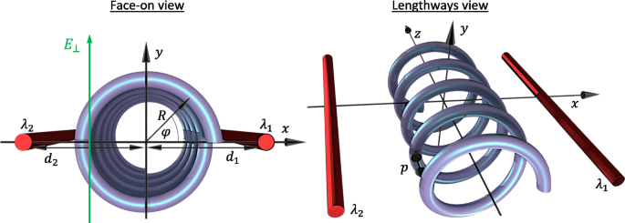
从正面和纵向角度的系统几何形状和参数图。 R 是螺旋半径,d 1 和 d 2 是带电导线到螺旋轴的距离,电荷密度为λ 1 和 λ 2、分别。空间坐标φ 从正面描述螺旋上的角位置并与 z 有关 -坐标通过φ =2π z /p 与 p 螺旋的螺距。横向电场E ⊥ 平行于 y -轴
我们已经几何重整化了电子有效质量 M e M * =M e (1+R 2 /ρ 2 ) 为了用沿螺旋轴的坐标来表达一切(回想一下 φ =z /ρ ) 对外部电位更方便。在这里,V ⊥(φ )=-eE ⊥R sin(φ ) 是沿 y 方向的横向电场的贡献 -axis 使得 V ⊥(π /2)<0。栅极的电位为 V g (φ )=−e [Φ 1(φ )+Φ 2(φ )] 由于由 Φ 给出的单独带电导线,电子沿螺旋线感受到的静电势 我 (φ )=−λ 我 k ln(r 我 /d 我 )。在这里,i =1,2 标记电线,λ 我 是导线上的线性电荷密度,\(k =1/2\pi \tilde {\epsilon }\) 和 \(\tilde {\epsilon }\) 是绝对介电常数。测试电荷与特定导线的垂直距离为 \(r_{i}=[d^{2}_{i}+R^{2} + 2(-1)^{i}d_{i }R\cos (\varphi)]^{1/2}\),带有 d 我 表示线到螺旋轴的相应距离。我们已将零栅极诱导电位定义为沿螺旋轴。一维总势V T (φ )=V g (φ )+V ⊥(φ ) 显然是周期性的 V T (φ )=V T (φ +2π n ) 周期为 2π 一般来说(对应于 p 相对于坐标 z )。这个周期明显大于原子间距离,并产生典型的超晶格效应。这个字母不同于横向电场中的纳米螺旋(可以用 V T (φ )=V ⊥(φ ) 此处) 主要是通过双栅电势 V 操纵超晶格的重复晶胞 g (φ )。取极限 p →0,我们回到受两个静电门影响的环形图片上的粒子 [63, 64]。进行近似 R /d 我 ≪1,我们可以展开V g (φ ) cos(φ ),并在变换方程。 1 变成无量纲形式我们来
$$ {\begin{aligned} \frac{d^{2} \psi_{\nu}}{d\varphi^{2}}+\left[\epsilon_{\nu} + 2A_{g}\cos( \varphi) + 2B_{g}\cos(2\varphi) + 2C_{\bot} \sin(\varphi) \right]\psi_{\nu} =0, \end{aligned}} $$ (2)以能量标度为单位的数量 \(\varepsilon _{0}(\rho) =\hbar ^{2} / 2 M^{*} \rho ^{2}\) 定义为
$$\begin{array}{@{}rcl@{}} A_{g} &=&\beta\frac{\left(d_{1}^{2} +R^{2}\right)}{ d_{1} R}(1-\gamma), \qquad B_{g} =\frac{\beta}{2}\left(1+\frac{\lambda_{1}}{\lambda_{2}} \gamma^{2}\right), \\ C_{\bot} &=&e E_{\bot} R /2\varepsilon_{0}(\rho), \qquad \qquad \qquad \; \epsilon_{\nu} =\frac{\varepsilon_{\nu}}{\varepsilon_{0}(\rho)}。 \end{array} $$ (3)这里,\(\beta =ek d_{1}^{2} R^{2} \lambda _{1} /2\left (d_{1}^{2} +R^{2}\right)^ {2}\varepsilon _{0}(\rho) \) 表征来自门 1 的贡献,而不对称参数 \(\gamma =\lambda _{2} d_{2} \left (d_{1}^{2 } +R^{2}\right)/\lambda _{1} d_{1} \left (d_{2}^{2} + R^{2}\right)\) 表征门 2 的相对贡献, 与 γ =1 对应于对电位的相等门贡献(导致 A g =0)。需要注意的是,d难以维护造成的不对称性不可避免 1=d 2 可以通过操纵 λ 来补偿 1 和 λ 2. 在这封信中,我们限制自己考虑γ ≤1(即 |Φ 1|>|Φ 2|) 因为大于单位的不对称参数可以通过简单交换标记门的索引和相应的视角偏移 φ 映射到单位以下的等效系统 →φ ±π .我们也将只考虑 C ⊥≥0 由于负 C 的对称性 ⊥ 关于 φ 中的这种坐标平移 , 和 A g ≥0,B g>0(即只有导线上的正电荷密度 β>0) 因为任何带有负电门的潜在景观都可以通过正电门的参数的正确组合来再现。在图 2 中,我们绘制了无量纲势 V T (φ )/ε 0(ρ ),随着 π 的强度 - 固定在 B 的周期性电位分量 g =0.2,对于倍周期扰动参数A的几种组合 g 和 C ⊥.我们看到总的外部电位沿 φ 诱导了一个二元超晶格 ,双量子阱 (DQW) 作为单位单元以蓝色突出显示。这可以通过操纵相对门贡献γ而采用不同的形式 和横向电场E ⊥.晶胞本质上是一个在等效栅极贡献下的单井 (γ =1) 并且没有横向电场E ⊥=0(如图2a中A g =C ⊥=0)。修复 E ⊥=0,具有更强的门 1 贡献 (γ <1),晶胞变成具有不同阱最小值和退化势垒最大值的 DQW(图 2b,其中 A g =0.1 和 C ⊥=0)。相比之下,保持 DQW 最小值退化并相对于彼此操纵两个势垒需要对称的栅极贡献(γ =1) 在非零电场 E ⊥≠0 (Fig. 2c with A g =0 和 C ⊥=0.1)。结合非对称门贡献(γ <1) 与 E ⊥≠0 产生具有不同势阱最小值和不同势垒的 DQW(如图 2d 所示,其中 A g =C ⊥=0.1)。正如我们将在以下部分中看到的,这会导致性质上不同且丰富的行为。
<图片>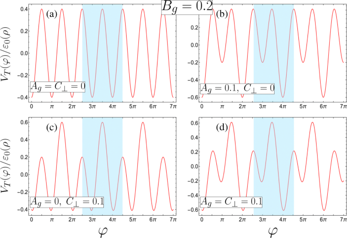
四种可能的超晶格势配置,其中单位单元以蓝色突出显示(根据无量纲参数定义,物理参数的相应要求参见方程 3,并且都带有 B g =0.2)。 一 一元超晶格在晶胞中具有退化的最小值和最大值 (A g =C ⊥=0)。 b –d 由 b 形成的二元超晶格 由于退化最大值 (A g =0.1,C ⊥=0), c 仅具有退化最小值的对称 DQW (A g =0, C ⊥=0.1) 或 d 具有不同最小值和最大值的非对称 DQW (A g =C ⊥=0.1)
作为无限矩阵的解
方程的解决方案。 2 可以在Bloch函数方面找到
$$ \psi_{n,q}(\varphi)=(2\pi N \rho)^{-\frac{1}{2}}e^{iq \varphi}\sum_{m} c^{( n)}_{m,q} e^{im \varphi}, $$ (4)其中 q =k z ρ 是电子拟动量 k 的无量纲形式 z 沿螺旋轴,n 表示子带,前因数来自 φ 方面的归一化 :\(\rho \int _{0}^{2\pi N}|\psi _{n,q}(\varphi)|^{2} d\varphi =1\)。我们通过将结果表达式乘以 \(e^{im^{\prime } \varphi }/2\pi \) 并相对于 φ 积分来利用指数函数的正交性 , 其中 m ′ 是一个整数,这样我们就可以得到系数 \(c^{(n)}_{m,q}\),
的无限联立方程组 $$ {\begin{aligned} &\left[(q+m)^{2}-\epsilon_{n}\right]c^{(n)}_{m} - \left(A_{g} - i C_{\bot} \right)c^{(n)}_{m-1} - \left(A_{g} + i C_{\bot} \right)c^{(n)}_{m +1}\\ &\quad- B_{g}\left(c^{(n)}_{m+2}+c^{(n)}_{m-2} \right)=0, \结束{对齐}} $$ (5)为清楚起见,q -下标符号已被删除,ε n,q ≡ε n 和 \(c_{m}^{(n)}\equiv c_{m,q}^{(n)} \)。方程 5 表示无限五对角矩阵,其中很明显系统在 q 中是周期性的 ,我们可以将我们的考虑限制在由 − 1/2≤q 定义的第一个布里渊区 ≤1/2。在没有超晶格势A g =B g =C ⊥=0,则特征值由m枚举 由 ε 给出 米 =(米 +q ) 2 我们认识到 m 是与螺旋上的自由电子相关的角动量量子数。我们从方程中看到。 5 当 A g =C ⊥=0 仅具有 Δ 的状态 米 =±2 是混合的,而通过 A 实现的具有不同阱最小值或势垒的 DQW 晶胞的形成 g ≠0 和/或 C ⊥≠0,也与Δ混合状态 米 =± 1. 有趣的是,在外部横向电势(在螺旋的一圈内变化)下,螺旋上的电子系统在数学上等效于被磁场穿透并受到一个电势的量子环上的电子相同的函数形式沿角坐标变化;例如见参考。 [65–67] 或比较例如参考文献。 [42-45] 与 [68-70]。对于环,q所起的作用 这里被磁通量占据。因此,这项工作中完全相同的分析适用于双门量子环的问题[63-66],如果环被磁通量穿透。
截断和数值对角化对应于方程的矩阵。 5 提供了 n 第 子带特征能量 ε n q 的每个值的系数 \(c_{m}^{(n)}\) .我们在 |m 处应用截断 |=10,知道矩阵大小的任何增加都不会在最低子带中产生明显的变化。
结果与讨论
双门控纳米螺旋带结构
我们在图 3 中绘制了几种参数组合的最低波段的能量色散。根据超晶格的形式,我们发现色散行为存在显着差异,对于一些特定的参数组合,我们发现布里渊区边缘(图 3a 和 c)或布里渊区的中心(图 3b 和 d)。
<图片>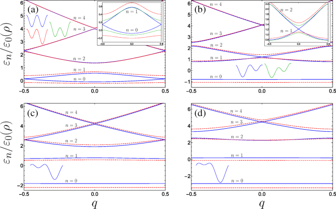
无量纲参数的各种组合的双门控纳米螺旋系统的能带结构(带有 B g =0.4 固定):a 纯蓝色(红色虚线)图 A g =0 &C ⊥=0 (A g =0.2 &C ⊥=0),插图还绘制了底部两个子带在具有 A 的横向电场下的行为 g =0 &C ⊥=0.2 为点划绿色曲线。 b 纯蓝色(红色虚线)图 A g =0.63 &C ⊥=0 (A g =0.8 &C ⊥=0) 其中蓝色曲线描绘了第一次共振事件(见正文),能带在布里渊区的中心交叉,插图将底部激发的两个子带的行为与 A g =0.63 &C ⊥=0.2 为点划绿色曲线。 c 纯蓝色(红色虚线)图 A g =1.26 &C ⊥=0 (A g =1.5 &C ⊥=0),其中蓝色曲线描绘了第二次共振,在较高能带的布里渊边缘处能隙关闭。 d 第三个共振和更高的子带小间隙靠近中心,纯蓝色(红色虚线)是 A g =1.9 &C ⊥=0 (A g =2.2 &C ⊥=0)。单元格形状是草图,n 枚举bands,insets轴与主图一致
低场倍周期扰动
当 A g =C ⊥=0,晶胞构成两个等效的量子阱,因此自然出现在布里渊区边缘接触的能带对。事实上,只取一个井作为单位单元将超晶格周期减半并导致布里渊区加倍 - 1≤q ≤1。然后我们将观察通常的一元超晶格带图,其中在 q 处的地面和第一带之间的带隙 =1 在这里通过 n 之间的带隙给出 =1 和 n =2 在 q =0 并且在 B 中是线性的 g 来自微扰理论。尽管如此,我们仍然描述了 |q 处的能带结构 附录中使用矩阵代数的 DQW 晶胞图片中 |=1/2。如图 3a 的插图所示,双周期电位项之一的引入在布里渊区边缘打开了带隙。对称门贡献的晶胞 (A g =0) 在横向场 C 的应用下保持对称 DQW 的形式 ⊥ 垂直于螺旋门轴,一个势垒相对于另一个进行了修改(由图 3a 上的绿色 DQW 草图表示)。而 C ⊥ 打开了一个带隙,色散的改变明显不如施加的相似幅度的 A 敏感 g .这可以从 |q 处的较小带隙看出 |=1/2 对于图 3a 插图中的点划绿线(带有 A g =0 和 C ⊥=0.2) 与红色虚线的较大差距(对于 A g =0.2 和 C ⊥=0)。为了强调这种行为,图 4a 绘制了 |q 处的能隙大小 |=1/2 在两个最低子带之间 \(\Delta \varepsilon _{01}^{(q=1/2)}/\varepsilon _{0}(\rho)\) 对于固定的 B g =0.25 作为 C 的函数 ⊥ (与 A g =0) 和 A g (使用 C ⊥=0),分别为绿色虚线和红色虚线。在零横向电场和非对称栅极电位 (C ⊥=0 和 A g ≠0),则晶胞是不对称的 DQW,尽管由于等效势垒而具有关于任一阱最小值的内部反射对称性。然后我们可以理解带隙对改变 A 的更高敏感性 g 通过考虑构建超晶格的隔离 DQW 晶胞的特性。随着 A g =C ⊥=0,在 |q |=1/2(布里渊区的边缘),由隔离 DQW 晶胞的基态和第一激发态形成的布洛赫态(参见图 4a 中的蓝色示意图和伴随波函数)将仅相差任意相。这种情况对应于图 3a 的无间隙蓝色色散曲线。如图 4a 中通过绿色 DQW 草图示意性描绘的,C ⊥ 减少了一个障碍相对于另一个障碍的相对最大值,而 DQW 最小值保持退化。因此,隔离 DQW 的基态仅通过其在较小势垒下的概率分布略有增加(与未受干扰的基态相比仅产生很小的能量降低)而被修改,并且第一激发态基本保持不变因为它的节点位于屏障下方并且对其变化不敏感。由这些基态和第一激发态构成的布里渊区边缘的布洛赫态与未受扰情况的不同之处仅在于在较小势垒下基态波函数的衰减减少(比较绿色 DQW 和蓝色 DQW图 4a)。改变 A g 操纵 DQW 最小值的相对位置,同时保持障碍退化。两个最低隔离 DQW 态的波函数差异很大,基态趋向于单个深井的局部基态,而第一激发态趋向于较浅阱的局部基态 [71]。虽然扰动降低了基态能量,但随着A的增加,浅阱的最小值上移,第一激发态的能量相对增加 g ,导致带隙大小相对于 A 的更高灵敏度 g .特别是,随着 A 的增加,地面子带中的粒子迅速发现自己被限制在最深势阱底部附近 g .因此,最低能带比横向场情况下更快地接近无色散平带,这可能导致电子不稳定性和伴随高态密度的强相互作用效应[72]。
<图片>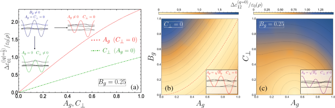
一 地面和第一子带之间的带隙大小作为 A 的函数 g (C ⊥) 绘制为红色虚线(绿色点划线),这里 B g =0.25。这些图表明了不同扰动对孤立的 DQW 晶胞和本征态的影响。 b –c 第一和第二子带之间的带隙大小通过二维密度图表示为: b A g 和 B g 对于 C ⊥=0,并且 c A g 和 C ⊥ 带有固定的 B g =0.25。 b 相邻的等能等值线表示 0.17 的差异,零间隙由 \(A_{g}=\sqrt {B_{g}}\) 的点划红线给出,而 c 差异为 0.13,最小半圆轮廓 (0.5,0) 中心处的间隙为零。这些图描绘了孤立的 DQW 和本征态。 s之间不发生杂交 -like 和 p -b 中类似共振局部化的单个阱状态 , 但在 c 中 由于电场改变一个势垒相对于另一个势垒
能带交叉
值得注意的是,如果我们保持 C ⊥=0 并增加 A g ,虽然最初所有简并都被解除,但随后的更高能带在布里渊区的中心和边缘之间交替交叉(观察从图 3a 到 d 的交替蓝色和红色虚线曲线的行为)。从物理上讲,我们可以根据晶胞中局部波函数的相互作用来理解消失带隙。当不对称 DQW 电位使得较浅阱中的基态 (s -like 轨道)与较深井中的第一个激发态共振(p - 类似轨道),在 q =0 由于关于任一阱中心的反射对称性,这些状态的相反奇偶性阻止了它们之间通常的隧道耦合,因此由这些轨道构建的激发态重合(图 3b 中的蓝色曲线)。这让人想起所谓的s -p 光晶格中的共振 [73, 74]。同理,如果参数使得浅阱中的局域基态与具有相同奇偶性的深阱中的激发态共振,则在 |q |=1/2,Bloch 相的存在完全抑制了这两个相邻的局部阱态之间的通常杂交,并且带隙是闭合的(如图 3c 所示,用于地面与第二激发态的共振)。用周期性势能散射的语言;由于来自 cos(φ ) 来自 cos(2φ ) 潜力 [75–77]。
通过返回方程,我们可以定量地显示布里渊区中心和边缘处的能带交叉(对于零横向电场)的存在。 2,当 C ⊥=0 [78]。布洛赫函数方程。 4 服从扭曲周期边界条件ψ n,q (φ +2π )=exp(2π 智商 )ψ n,q (φ )。特别是当 q =0 方程的形式解。 2 是 2π - 周期性,而当 |q |=1/2 解是 2π -反周期(因此我们将搜索 4π - 定期解决方案)。具体来说,方程。 2 与 C ⊥=0 可以映射到 Ince 方程 [79, 80],通过将波函数表示为方程的渐近解的乘积,它是准精确解的。 2 和一个未知函数 \(\psi _{n,q}(\varphi) =\exp \left [ -2\sqrt {B_{g}}\cos (\varphi)\right ]\Phi _{n, q}(\varphi)\),使得
$$ \frac{d^{2} \Phi_{n,q}}{d \varphi^{2}} + \frac{\xi}{2} \sin(\varphi)\frac{d\Phi_{ n,q}}{d\varphi} +\frac{1}{4}\left[ \eta_{n,q} - p\xi\cos(\varphi) \right]\Phi_{n,q} =0, $$ (6)其中我们定义了辅助参数 \(\xi =8\sqrt {B_{g}}\), η n,q =4ε n,q +8B g , \(-p \xi =8A_{g}+8\sqrt {B_{g}}\) 和 Φ n,q (φ ) 保持每个解的必要扭曲周期(注意这里 p 不是 螺距)。另外,由于这里的超晶格势在变换φ下是不变的 →− φ , q 的解 =0 和 q =1/2 可以分为奇偶校验,使得下面的三角级数
$$ \Phi_{n,0}^{(e)}(\varphi) =\sum_{l=0}a^{(n)}_{l}\cos(l\varphi), $$ (7a ) $$ \Phi_{n,0}^{(o)}(\varphi) =\sum_{l=0}b^{(n)}_{l+1}\sin[(l+1)\ varphi], $$ (7b) $$ \Phi_{n,\frac{1}{2}}^{(e)}(\varphi) =\sum_{l=0}\widetilde{a}^{( n)}_{l}\cos\left[\left(l+\frac{1}{2}\right)\varphi\right], $$ (7c) $$ \Phi_{n,\frac{1} {2}}^{(o)}(\varphi) =\sum_{l=0}\widetilde{b}^{(n)}_{l+1}\sin\left[\left(l+\frac {1}{2}\right)\varphi\right], $$ (7d)覆盖了形式解,我们注意到 q 的解 =−1/2 与 q 相同 =1/2。这里,上标 e 和 o 分别将函数标记为偶数和奇数,并且 n 仍指 n 第 th 个子带,也是 n 这些指定的 q 的本征态 值。将这些代入方程。 6 得出傅立叶系数的三项递归关系。 q =0 偶数解产生
$$ -\eta_{n,0}^{(e)}a^{(n)}_{0} + \xi\left(\frac{p}{2} +1 \right) a^{( n)}_{2} =0, $$ (8a) $$ \xi pa^{(n)}_{0} + \left(4 - \eta_{n,0}^{(e)} \ right)a^{(n)}_{2} + \xi \left(\frac{p}{2} +2 \right)a^{(n)}_{4}=0, $$ (8b ) $$ {\begin{aligned} &\xi \left(\frac{p}{2} - l +1 \right)a^{(n)}_{2l-2} + \left(4l^{ 2} - \eta_{n,0}^{(e)} \right)a^{(n)}_{2l}\\ &\quad+\xi \left(\frac{p}{2} + l +1 \right)a^{(n)}_{2l+2} =0, \qquad (l \ge 2) \end{aligned}} $$ (8c)以及 q 奇解的对应递归关系 =0 是
$$ (4 - \eta_{n,0}^{(o)})b^{(n)}_{2} + \xi \left(\frac{p}{2} +2 \right)b ^{(n)}_{4} =0, $$ (9a) $$ {\begin{aligned} &\xi \left(\frac{p}{2} - l +1 \right)b^{ (n)}_{2l-2} + \left(4l^{2} - \eta_{n,0}^{(o)} \right)b^{(n)}_{2l} +\xi \left(\frac{p}{2} + l +1 \right)b^{(n)}_{2l+2}\\ &=0. \qquad (l \ge 2) \end{aligned} } $$ (9b)q =1/2 偶数解给出
$$ \left[ 1 -\eta_{n,\frac{1}{2}}^{(e)} +\frac{\xi}{2}(p+1) \right]\widetilde{a} ^{(n)}_{1} +\frac{\xi}{2}(p+3)\widetilde{a}^{(n)}_{3}=0, $$ (10a) $$ {}{\begin{aligned} &\frac{\xi}{2}(p-2l +1)\widetilde{a}^{(n)}_{2l-1}+\left[(2l+1) )^{2} - \eta_{n,\frac{1}{2}}^{(e)}\right]\widetilde{a}^{(n)}_{2l+1}\\ &\ quad+ \frac{\xi}{2}(p+2l+3)\widetilde{a}^{(n)}_{2l+3}=0, \qquad (l \ge 1) \end{aligned} } $$ (10b)和 q =1/2 奇解给出
$$ \left[ 1 -\eta_{n,\frac{1}{2}}^{(e)} -\frac{\xi}{2}(p+1) \right]\widetilde{b} ^{(n)}_{1} +\frac{\xi}{2}(p+3)\widetilde{b}^{(n)}_{3}=0 $$ (11a) $$ { }{\begin{aligned} &\frac{\xi}{2}(p-2l+1)\widetilde{b}^{(n)}_{2l-1}+\left[(2l+1) ^{2} -\eta_{n,\frac{1}{2}}^{(e)}\right]\widetilde{b}^{(n)}_{2l+1}\\&\quad + \frac{\xi}{2}(p+2l+3)\widetilde{b}^{(n)}_{2l+3}=0. \qquad (l \ge 1) \end{aligned}} $$ (11b)Consider then Eqs. (8c) and (9b) for the q =0 solutions. The series solutions (7a) and (7b) can clearly be made to terminate if p is 0 or an even positive integer. The resulting polynomials are referred to as Ince polynomials. The remaining solutions for higher eigenvalues are simultaneously double degenerate and correspond to the energy crossings observed at q =0 for certain parameters. The existence of these degeneracies can be seen by looking at the diagonalizable matrices describing the recursion relations for a l 和 b l :
$$ \boldsymbol{\mathcal{A}} =\left[ \begin{array}{ccccc} 0 &\xi\left(\frac{p}{2} +1 \right) &0 &0 &\hdots \\ \xi p &4 &\xi\left(\frac{p}{2} +2 \right) &0 &\hdots \\ 0 &\xi\left(\frac{p}{2} - 1 \right) &16 &\xi\left(\frac{p}{2} +3 \right) &\hdots \\ \vdots &\vdots &\vdots &\vdots &\ddots \end{array} \right]\!, $$ (12)和
$$ \boldsymbol{\mathcal{B}} =\left[ \begin{array}{ccccc} 4 &\xi\left(\frac{p}{2} +2 \right) &0 &0 &\hdots \\ \xi\left(\frac{p}{2} - 1 \right) &16 &\xi\left(\frac{p}{2} +3 \right) &0 &\hdots \\ 0 &\xi\left(\frac{p}{2} -2 \right) &36 &\xi\left(\frac{p}{2} +4 \right) &\hdots \\ \vdots &\vdots &\vdots &\vdots &\ddots \\ \end{array} \right]\! $$ (13)分别。 Either of the above tridiagonal matrices can be broken into tridiagonal sub-matrices if a leading off-diagonal matrix element is equal to zero, i.e. if p is an even number. The matrices will decompose into two tridiagonal blocks, one smaller finite matrix \(\boldsymbol {\mathcal {A}_{1}}\) (\(\boldsymbol {\mathcal {B}_{1}}\)) and a remaining infinite matrix \(\boldsymbol {\mathcal {A}_{2}}\) (\(\boldsymbol {\mathcal {B}_{2}}\)). From the theory of tridiagonal matrices the corresponding eigenvalue spectra for each matrix is then \(\eta (\boldsymbol {\mathcal {A}}) =\eta (\boldsymbol {\mathcal {A}_{1}}) \cup \eta (\boldsymbol {\mathcal {A}_{2}})\) and \(\eta (\boldsymbol {\mathcal {B}}) =\eta (\boldsymbol {\mathcal {B}_{1}}) \cup \eta (\boldsymbol {\mathcal {B}_{2}})\). The smaller finite matrices are analytically diagonalizable in principle, giving exact eigenvalues, and their corresponding finite length eigenvectors define the fourier coefficients yielding Ince polynomials via Eq. 7. We can see that for a given even integer p , the remaining infinite tridiagonal matrices are the same \(\boldsymbol {\mathcal {A}_{2}}=\boldsymbol {\mathcal {B}_{2}}\equiv \boldsymbol {\mathcal {D}}\) which results in the double degenerate eigenvalues. To be clear, we provide an example of when p =2 in the Appendix.
In the same way, when p is a positive odd integer the series solutions (7c) and (7d) can be made to terminate, and the matrices corresponding to \(\widetilde {a}_{l}\) and \(\widetilde {b}_{l}\) share eigenvalues resulting in the closing of higher subbands at the edge of the Brillouin zone q =± 1/2. From the definitions of the auxiliary parameters in Eq. 6, we have
$$ A_{g} =(p+1)\sqrt{B_{g}}, $$ (14)which defines the condition for exactly-solvable solutions for the lower lying solutions and simultaneously the existence of higher double degenerate eigenvalues above the p th subband, with p =0 or an even positive integer corresponding to crossings at the centre of the Brillouin zone, while crossings at the edge require p to be an odd positive integer. Figure 4b plots the size of the band gap between the first and second subbands \(\Delta \varepsilon _{12}^{(q=0)}/\varepsilon _{0}(\rho)\) as a function of A g 和 B g , with the dot-dashed red contour line corresponding to Eq. 14 for p =0。 The schematic indicates the appropriate eigenstates of the isolated DQW at the p =0 resonance.
The application of a small transverse field C ⊥ breaks the reflection symmetry of the system, permitting hybridization of the localized well states of the isolated DQW which results in a significant change at points of degeneracy, as can be seen by comparing the schematic depicted in Fig. 4b with that in c (see also inset of Fig. 3b). We plot in Fig. 4c the behaviour of the band gap between the first and second subbands as a function of A g 和 C ⊥. Here we see that the band gap is more sensitive to C ⊥ due to the significant change in the isolated DQW eigenstates by lowering one barrier with respect to the other. This behaviour is notably the converse of the parameter sensitivity for the band gap between the ground and first subbands. By degenerate perturbation theory, it can be shown that this induced band gap is linear in C ⊥ for the lowest crossing bands when p =0, and to higher order with increasing p . Finally, within the vicinity of the crossings, e.g. for small q about q =0 in Fig. 3a, the dispersions could be approximated as a quasi-relativistic linear dispersion yielding Dirac-like physics, which could permit superfluiditiy [81] for example. The advantage in using nanohelices lies in introducing such phenomena to portable nanostructure based devices, while also exhibiting unusual responses of the charge carriers to circularly polarized radiation [44, 45, 82–85] (or indeed magnetic fields [86, 87]) due to the helical spatial confinement.
Optical transitions
In order to understand how our double-gated nanohelix system interacts with electromagnetic radiation, we study the inter-subband momentum operator matrix element \(T^{g\rightarrow f}_{j} =\langle {f}|\boldsymbol {\hat {j}} \cdot \boldsymbol {\hat {P}}_{j} |{g}\), which is proportional to the corresponding transition dipole moment, and dictates the transition rate between subbands ψ f and ψ g . Here, \(\boldsymbol {\hat {j}}\) is the projection of the radiation polarization vector onto the coordinate axes (j =x,y ,z ) and the respective self-adjoint momentum operators are [44, 45, 82–84]
$$ \boldsymbol{\hat{P}}_{x} =\boldsymbol{\hat{x}}\frac{i \hbar R}{\rho^{2} +R^{2}}\left[\sin(\varphi)\frac{d}{d\varphi} + \frac{1}{2}\cos(\varphi) \right], $$ (15a) $$ \boldsymbol{\hat{P}}_{y}=-\boldsymbol{\hat{y}}\frac{i \hbar R}{\rho^{2} +R^{2}}\left[\cos(\varphi)\frac{d}{d\varphi} - \frac{1}{2}\sin(\varphi) \right], $$ (15b) $$ \boldsymbol{\hat{P}}_{z}=-\boldsymbol{\hat{z}}\frac{i \hbar \rho}{\rho^{2} +R^{2}}\frac{d}{d\varphi}. $$ (15c)In terms of the dimensionless position variable φ , we are required to evaluate \(T^{g\rightarrow f}_{j} =\rho \int _{0}^{2\pi N}\psi _{f}^{\ast } P_{j} \psi _{g} d\varphi \), and upon substituting in from Eq. 4 we find
$$ {\begin{aligned} T^{g\rightarrow f}_{x} &=\frac{i \hbar R}{2\left(\rho^{2} + R^{2} \right)}\sum_{m} c_{m}^{\ast (f)} \left[ c_{m-1}^{(g)} \left(q+m-\frac{1}{2}\right)\right.\\ &\quad\left.-c_{m+1}^{(g)} \left(q+m+\frac{1}{2}\right) \right], \end{aligned}} $$ (16a) $$ {\begin{aligned} T^{g\rightarrow f}_{y} &=\frac{\hbar R}{2\left(\rho^{2} + R^{2} \right)}\sum_{m} c_{m}^{\ast (f)} \left[ c_{m-1}^{(g)} \left(q+m-\frac{1}{2}\right)\right.\\&\left.\quad+c_{m+1}^{(g)} \left(q+m+\frac{1}{2}\right) \right], \end{aligned}} $$ (16b) $$ T^{g\rightarrow f}_{z} =\frac{\hbar \rho}{\left(\rho^{2} + R^{2} \right)} \sum_{m} c_{m}^{\ast (f)} c_{m}^{(g)} (q+m). $$ (16c)We see from Eqs. 16a and 16b that light linearly polarized transverse to the helix axis couples coefficients with angular momentum differing by unity Δ 米 =± 1, whereas from Eq. 16c, linear polarization parallel to the helix axis couples only Δ 米 =0。 In Fig. 5, we plot the absolute square of the momentum operator matrix element between the lowest three bands for linearly polarized light propagating perpendicular to the helix axis (i.e. with z -极化)。 Initially, for A g =C ⊥=0, transitions between the ground and first bands are forbidden (as is to be expected for a unit cell with two equivalent wells resulting in a doubling of the first Brillouin zone, so it is in fact the same band). As the strength of the doubled period potential A g is increased with respect to B g , transitions become allowed away from q =0 as can be seen from Fig. 5a (following behaviour from the dotted red curve through to the solid blue curve). The parameters are swept through a resonance as we go from the solid to the dashed blue curve, wherein the situation changes drastically. To understand this behaviour, we must consider the special case of q =0。 As we traverse this resonance, the energy of the Bloch function with q =0 constructed from the first excited state of the deeper well in the DQW unit cell (p -like) passes below the Bloch function constructed from the ground state in the shallower well (s -like). Consequently, the parity with respect to φ (which is a good quantum number only for q =0 or |q |=1/2) of the two excited states is exchanged resulting in the rapid switch from forbidden to allowed at q =0, wherein the z -polarized inter-subband matrix element becomes non-zero due to the operator \(\boldsymbol {\hat {P}}_{z}\) (see Eq. 15c) now coupling the even ground state with the odd first excited state. We therefore see the opposite behaviour for transitions between the ground and second band in Fig. 5b about q =0。 While initially increasing A g allows transitions at q =0 between the ground state and the second excited state when it is p -like, beyond resonance (when the order of the s -like and p -like excited states are swapped) transitions are suppressed. See for example Ref. [88] for a clear picture of this interchange between the ordering of the even and the odd parity excited states. For transitions between the first and second band (Fig. 5c), we observe a large transition centred about q =0 due to the lifting of the m =± 1 degenerate states of the field-free helix by the superlattice potential. The presence of symmetry-breaking C ⊥ ruins the pristine parities of the states at the centre of the Brillouin zone and all transitions are allowed, as shown in the insets of Fig. 5.

Square of the dimensionless momentum operator matrix element between the g th and f th subbands in the first Brillouin zone as a function of the dimensionless wave vector q of the electrons photoexcited by linearly z -polarized radiation and for a variety of parameter combinations spanning the first incident of resonance. The different blue curves keep A g =0.5 and C ⊥=0 fixed and vary B g =0.1, 0.2, and 0.3 corresponding to dot-dashed, dashed, and solid. The different red curves keep B g =0.3 and C ⊥=0 fixed while varying A g =0.05, 0.1 and 0.3 as dot-dashed, dashed, and solid, while the dotted blue (dotted red) plots the limiting case A g =0.5 &B g →0 (A g →0 &B g =0.3). 一 Transitions between the ground and first bands. The inset plots the behaviour for fixed A g =0.5 and changing B g crossing the resonant condition at B g =0.25 (see text) in a reduced q -range, ranging from upper blue B g =0.245, lower blue B g =0.249, upper purple B g =0.251, to lower purple B g =0.255. The dashed green curves are for small non-zero transverse field C ⊥=0.05 ranging from B g =0.245 (upper curve) to B g =0.255 (lower curve) in increments of 0.05. b Plots transitions between the ground and second bands, the inset plots the behaviour close to resonance when A g =0.5; blue is B g =0.249, purple is B g =0.251, and dark green is at resonance with C ⊥=0.05. c Plots transitions between the first and second bands, the parameters for the inset are the same as those in (b )
In Fig. 6, we plot the absolute square of the momentum operator matrix element for right-handed circularly polarized light which propagates along the helix axis, given by |T x +iT 是 | 2 . Notably, we observe a large anisotropy between the two halves of the first Brillouin zone, while the result for left-handed polarization is a mirror image to what we see in Fig. 6. Physically, this can be attributed to the conversion of the photon angular momenta to the translational motion of the free charge carriers projected onto the direction of the helix axis, with an unequal population of the excited subband in a preferential momentum direction controlled by the relative handedness of both the helix and the circular polarization of light. An intuitive mechanical analogue would be the rotary motion of Archimedes’ screw being converted into the linear motion of water along the direction of the screw axis dictated by the handedness of the thread. As such, our system of a double-gated nanohelix irradiated by circularly polarized light exhibits a photogalvanic effect, whereby one can choose the net direction of current by irradiating with either right- or left-handed circularly polarized light [44, 45, 89]. This differs from conventional one-dimensional superlattices, wherein the circular photogalvanic effect stems from the spin-orbit term appearing in the effective electron Hamiltonian and is consequently a weaker and hard-to-control phenomenon [90, 91]. The electric current induced by promoting electrons from the ground subband to an excited subband f via the absorption of circularly polarized light can be understood from the equation for the electric current contribution from the f th subband
$$ j_{f} =\frac{e}{2 \pi \rho} \int dq \left[ v_{f}(q) \tau_{f}(q) - v_{g}(q) \tau_{g} (q) \right] \Gamma_{CP}^{g \rightarrow f}(q), $$ (17)
Square of the dimensionless momentum operator matrix element between the g th and f th subbands in the first Brillouin zone as a function of the dimensionless wave vector q of the electrons photoexcited by right-handed circularly polarized radiation |T x +iT 是 | 2 and for a variety of parameter combinations spanning the first incident of resonance. 一 The blue curves denote transitions between the ground and first band while the red curves denote transitions between the ground and second band, both with the following parameters:A g =0.5 and B g =0.3 for solid curves, A g =0.5 and B g =0.1 for dashed curves, A g =0.3 and B g =0.3 for dot-dashed curves, and A g =0.01 and B g =0.3 for dotted curves (as A g →0 the maximum of the 0→2 increases rapidly as it approaches q =− 1/2). The inset plots the behaviour as B g is tuned through resonance for A g =0.5; dotted is B g =0.24, dot-dashed is B g =0.25, and dashed is B g =0.26. The solid purple (orange) curve denotes transitions between the ground and first (second) band at resonance with C ⊥=0.05 applied. b Plots transitions between the first and second bands. The different blue curves keep A g =0.5 fixed and vary B g =0, 0.2, and 0.3 corresponding to dotted, dot-dashed, and solid. The different red curves keep B g =0.3 fixed while varying A g =0.05, 0.1, and 0.3 as dotted, dot-dashed, and solid. We have omitted plots for C ⊥≠0 here as it yields no great qualitative change to the matrix elements
where \(v_{g,f}(q)=(\rho /\hbar)\partial \varepsilon _{g,f}/\partial q \) is the antisymmetric electron velocity v (q )=− v (− q ) (which we can deduce from the symmetric dispersion curves), τ g,f (q ) is a phenomenological relaxation time, and \(\Gamma _{CP}^{g \rightarrow f}(q)\) is the transition rate resulting from the optical perturbation of the electron system. Given that \(\Gamma _{CP}^{g \rightarrow f}(q) \propto |T_{x}^{g \rightarrow f} + i T_{y}^{g \rightarrow f}|^{2}\) for right-handed circularly polarized light where T x and T 是 are given by Eqs. 16a and 16b, respectively. The anisotropy present in Fig. 6a enters Eq. 17 to yield a non-zero photocurrent. This current flows in the opposite direction for left-handed polarization. Such a circular photogalvanic effect is also exhibited in chiral carbon nanotubes under circularly polarized irradiation [92, 93], although tunability predominantly stems from manipulating the nanotube physical parameters, which are hard to control. The double-gated nanohelix system offers superior versatility by fully controlling the landscape of the superlattice potential, which can be used to tailor the non-equilibrium asymmetric distribution function of photoexcited carriers (as shown in Fig. 6 for inter-subband transitions between the three lowest subbands).
On a side note, we expect that (as with chiral carbon nanotubes [93–95]) the application of a magnetic field along the nanohelix axis can take up the role played by circularly polarized radiation, whereby the current is induced by a magnetic-field-induced asymmetric energy dispersion—which in turn produces an anisotropic electron velocity distribution across the two halves of the Brillouin zone.
结论
In summary, we have shown that the system of a nanohelix between two aligned gates modelled as charged wires is a tunable binary superlattice. The band structure for this system exhibits a diverse behaviour, in particular revealing energy band crossings accessible via tuning the voltages on the gates. The application of an electric field normal to the plane defined by the gates and the helix axis introduces an additional parameter with which to open a band gap at these crossings. Engineering the band structure in situ with the externally induced superlattice potential along a nanohelix provides a clear advantage over conventional heterostructure superlattices with a DQW basis [96, 97]. Both systems can be used as high-responsivity photodetectors, wherein tailoring the band structure (to the so-called band-aligned basis [98–100]) can lead to a reduction in the accompanying dark current. Here control over the global depth of the quantum wells also permits versatility over the detection regime, which can lie within the THz range. We have also investigated the corresponding behaviour of electric dipole transitions between the lowest three subbands induced by both linearly and circularly polarized light, which additionally allows this system to be used for polarization sensitive detection. Finally, the ability to tune the system such that a degenerate excited state is optically accessible from the ground state, along with the inherent chirality present in the light-matter interactions, may make this a promising system for future quantum information processing applications [101]. It is hoped that with the advent of sophisticated nano-fabrication capabilities [102], fully controllable binary superlattice properties will be realized in a nanohelix and will undoubtedly contribute to novel optoelectronic applications.
Appendix
Touching energy bands at Brillouin zone boundary when A g =C ⊥=0
Here, we show using matrix algebra that in the picture of a binary superlattice pairs of subbands touch at the Brillouin zone edges if A g =C ⊥=0 and B g ≠0, as seen from the solid blue curves in Fig. 3a. Equation 5 is equivalent to the following N -by-N pentadiagonal matrix Hamiltonian with zeros on the leading sub- and superdiagonals:
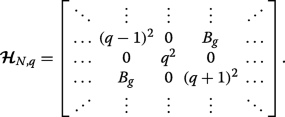 (18)
(18) Let us consider q =1/2 (we could alternatively take q =− 1/2) which makes the leading diagonal symmetric. We can then express this matrix Hamiltonian \(\widetilde {\mathcal {\boldsymbol {H}}}_{N} \equiv \boldsymbol {\mathcal {H}}_{N,q=1/2} \) in block form as
 (19)
(19) where
 (20)
(20) are both of dimension N /2-by- N /2, and J is the exchange matrix. We may construct a matrix via permuting \(\boldsymbol {\mathcal {H}}_{N}\) with the N -by-N permutation matrix \(\boldsymbol {\mathcal {P}}_{N}\),
$$ \boldsymbol{\mathcal{P}}_{N} =\left[ \begin{array}{cccccc} 1 &0 &\hdots &\hdots &\hdots &0 \\ 0 &\hdots &\hdots &\hdots &\hdots &1 \\ 0 &1 &\hdots &\hdots &\hdots &0 \\ 0 &\hdots &\hdots &\hdots &1 &0 \\ \vdots &&&&&\vdots \\ 0 &\hdots &\hdots &1 &\hdots &0 \\ \end{array} \right], $$ (21)such that the permutation-similar matrix is
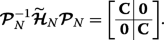 (22)
(22) Hence, the eigenvalues of \(\boldsymbol {\mathcal {P}}_{N}^{-1}\widetilde {\boldsymbol {\mathcal {H}}}_{N} \boldsymbol {\mathcal {P}}_{N}\), which are the same as the eigenvalues \(\widetilde {\boldsymbol {\mathcal {H}}}_{N}\), are double degenerate with the values given by the eigenvalue spectrum of the tridiagonal matrix C
 (23)
(23) which can also be expressed succinctly in terms of the previously defined matrices via \(\mathbf {C}=\boldsymbol {\mathcal {P}}_{N/2}^{-1}\mathbf {A}\boldsymbol {\mathcal {P}}_{N/2}+\boldsymbol {\mathcal {P}}_{N/2}^{-1}\mathbf {B}\mathbf {J}\boldsymbol {\mathcal {P}}_{N/2}^{4}\). We can see that applying C ⊥≠0 (inset of Fig. 3a) or both C ⊥ and A g ≠0 (inset of Fig. 3b) ruins the symmetry in the matrix Hamiltonian and prevents the existence of eigenvalues with multiplicity beyond unity, resulting in the appearance of band gaps.
Energy crossing at centre of Brillouin zone between third and forth subbands
As an example, let us specifically consider the case where p =2, wherein the matrices (12) and (13) become:
 (24)
(24) 和
 (25)
(25) This case corresponds to the crossings of the blue curves at the edge of the Brillouin zone in Fig. 3d (whereas p =0 results in crossings at q =0 in Fig. 3b). The lower eigenvalues are found exactly by diagonalizing each of the two finite matrices and they interlace, yielding \(\eta _{0,1,2} =2-\sqrt {4+4\xi ^{2}}, 4, 2+\sqrt {4+4\xi ^{2}}\). The infinite lower-right-hand block tridiagonal matrices coincide, thus the remaining double degenerate eigenvalues are found by approximately or numerically solving Det[D −η I ]=0.
数据和材料的可用性
The data for the figures all stem from numerically diagonalizing the matrix described by Eq. 5 and can readily be achieved in any numerical software package. With this in mind, the datasets used and/or analyzed during the current study are available from the corresponding author on reasonable request.
纳米材料