

通过多晶冲击波钻石的高温高压烧结制造的高质量发绿光纳米金刚石
摘要
我们展示了一种在纳米金刚石中形成氮空位氮中心的高压、高温烧结技术。平均尺寸为 25 纳米的多晶金刚石纳米颗粒前体是由爆炸产生的冲击波产生的。这些纳米粒子在乙醇的存在下,在 7GPa 的压力和 1300°C 的温度下烧结,以产生更大(3-4 倍)的金刚石微晶。记录的光谱特性表明结晶质量得到改善。还观察到存在的缺陷类型发生了变化;前体材料的氮空位和硅空位中心的特征光谱特征消失了。出现了两个新的特征:(1) 顺磁置换氮(P1 中心具有自旋 ½)由于 I 具有电子顺磁共振特征三重态超精细结构 =1 氮核自旋的磁矩和 (2) 氮空位氮中心的绿色光谱光致发光特征。这种生产方法是传统高能粒子束辐照的有力替代方法。它可以很容易地生产纯绿色荧光纳米金刚石,具有用于光学生物标记应用的有利特性。
介绍
氮杂质和空位是大多数天然和合成钻石的主要缺陷。单个缺陷可以共同形成具有多达 6 个亚基的缺陷复合体 [1, 2]。在这些缺陷复合物中,氮空位 (NV − ) 并且在较小程度上,氮空位氮 (NVN) 中心因其不闪烁的红色和绿色光致发光分别引起了极大的兴趣 [3, 4]。 NV − NVN 可以在纳米金刚石中可控地产生。纳米金刚石被广泛认为是无毒的纳米颗粒,因此可用作生物医学应用中的长期可追溯标记 [5]。具有 NV − 的纳米晶体 色心也用于量子传感[3]。
使用常规过渡金属溶剂催化剂高压、高温 (HPHT) 合成金刚石是标准的工业技术。许多实验室利用它来生长具有先进晶格参数的金刚石晶体。然而,近年来各种非常规金属催化剂开始得到广泛应用[6]。这种方法允许使用含氮有机添加剂和金属吸气剂在从高氮含量(高达 ~ 1000 ppm)到低得多的水平(~ 50 ppm)的范围内可控地掺杂金刚石 [7, 8] . HPHT还用于金刚石晶体的退火和改善晶体质量、脱色以及将纳米晶体烧结成更大的多晶体。
在温度(和压力)的影响下,金刚石中单个氮缺陷被分组为更大的复合物已被广泛研究。这种复合物可以作为特定的标记,记录完成结晶过程的温度历史 [1]。 NVN 和 NV − 可以通过用高能 (2–14 meV) 电子或质子或 ~ 40 keV 重离子照射原始含氮钻石来创建中心。辐照在金刚石晶格中产生空位。随后在 500-2000°C 范围内的温度下对样品进行退火会导致缺陷分组 [3, 9, 10]。目前,NV - 量产 或含 NVN 的纳米金刚石通常是通过高能电子辐照实现的。然而,这个过程既昂贵又耗时,并且需要特定的样品制备。因此,值得开发无需粒子照射的纳米金刚石色心生成替代方法。
最近引入了一种制造亚微米级金刚石晶体的新方法,该方法依赖于在 C-H-O 液体添加剂存在下烧结 5 纳米爆炸纳米金刚石 (DND) [11, 12]。在高温高压烧结条件下,添加的 C-H-O 有机物表现为超临界流体,可诱导金刚石快速再结晶。快速重结晶伴随着更高密度的空位 [13]。然而,这种方法会抑制前体 5 纳米 DND 中存在的原始色心 [14]。因此,需要一种可以在高温高压烧结过程中保留这些缺陷甚至产生其他类型缺陷的替代方法。
在这项工作中,我们使用通过爆炸辅助方法生产的前体多晶纳米金刚石,使用所谓的杜邦冲击波合成技术 [15,16,17]。我们在 C-H-O 添加剂的存在下以与现有专利程序相同的方式烧结这些纳米金刚石 [18](图 1),获得仅包含 NVN 色心的粗亚微米金刚石,而这些色心不存在于前体中纳米粒子。我们还跟踪所有 NV − 的演变 烧结前后颗粒中的 、P1 和 SiV 中心,使用电子顺磁共振 (EPR) 和荧光来证明烧结对存在的所有缺陷范围的影响。
<图片>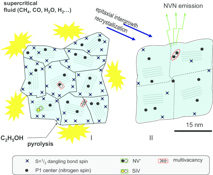
在高压和高温条件下烧结多晶金刚石颗粒以生产尺寸约为 30 nm 的亚微米金刚石纳米晶体的示意图。多晶(I)和高温高压烧结后的纳米晶(II)均观察到各种缺陷和色心
方法
样品制作
亚微米金刚石晶体是通过烧结平均尺寸为 25 纳米的市售前体多晶纳米金刚石(产品 DP 0-0.05,瑞士微金刚石)制备的。前体颗粒是通过爆炸辅助技术获得的,其中发生快速的、冲击波诱导的石墨到金刚石的转化(在 T 时在 100 微秒内发生) ≈ 950 °C,P ≈ 50 GPa)。爆炸产生的产物随后经过化学处理以净化金刚石纳米颗粒相,去除残留金属和无定形碳。该粉末由尺寸> 10μm的大多晶组成。按照先前描述的方法 [19],通过沿晶界研磨和解聚,这些多晶可以很容易地分馏。进行尺寸分级以提取形成 DP 0-0.05 多晶的小尺寸部分。最小部分的最终尺寸分布(图 2)在 27 nm 处具有最大值,半高宽 (FWHM) ≈ 25 nm(95% 的颗粒尺寸在 3-50 nm 范围内)。然后将选定的前体颗粒转移到环形高压室的内部石墨圆柱体中进行烧结。高压腔内部(即上述带有两个石墨盖的中空石墨圆柱体)的典型尺寸为:内径 4.0 毫米,高度 5.5 毫米。在烧结之前,将乙醇逐滴添加到干燥的纳米金刚石粉末中,直到完全填充颗粒间空间(约 30-50 重量%)[18]。然后在高压 (7GPa) 和高温条件 (1300 ± 50°C) 下烧结 10 秒。在一次印刷运行期间,可以处理约 ~ 120 毫克的前体金刚石粉末。高压室的方案可以在参考文献中找到。 [11].
<图片>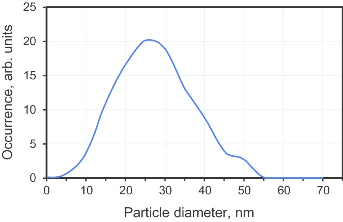
DP 0-0.05 多晶金刚石级分的粒度分布,平均粒度 ~ 27 nm,由差速离心沉降仪(CPS 盘式离心机,CPS Instruments Inc.,USA)测量
该烧结过程的效果如图 1 所示。在高温高压条件下烧结时,乙醇处于超临界状态。因此,它可以很容易地穿透多晶晶界,促进金刚石再结晶和新的金刚石相生长。烧结后,从高压室(此处标记为 D19)中提取出 ~ 90-100mg 质量可接受的白色金刚石粉末(没有石墨容器的污染)。烧结后粉末颜色从前体的灰色/黑色变为白色表明多晶表面的变化及其相应的生长[11]。
烧结前后材料的结构表征
多晶纳米金刚石前驱体的结构表征
我们首先在烧结前表征了 DP 0-0.05 的结构。 X 射线衍射 (XRD) 测量是使用 Rigaku Smart Lab III X 射线衍射仪进行的,使用 CuKα 辐射 (λ =1.54178 Å)。使用 40 kV 电压、30 mA 电流和 0.1 度/分钟的扫描速度。对于 2θ,DP 0-0.05 的 XRD 图如图 3(黑色)所示 在 6° 到 155° 的范围内。我们观察到六个峰,其中五个(111、220、311、400 和 331)是碳的金刚石相的特征。观察到的最强峰是立方金刚石 (D c ) 111 在 2θ ≈ 43.7°。该峰不对称,呈现左肩。用两个 Lorentzian 拟合该模式会产生以 2θ 为中心的第一个峰值 =43.76° 和 2θ 处的一秒 =41.64°。第一个峰对应于 (111) 金刚石平面的反射,而第二个(标记为 D H 011) 暂时归因于:(a) 六方 6H 多型金刚石相平面的反射 [20] 或 (b) 高应力下微晶之间的多个堆垛层错、孪晶和相关晶界。通过比较 D H 的积分 011 和 D c 111 个峰,我们估计 DP 0-0.05 前体中未识别的“相”(六边形或由结构缺陷组成)代表 ≈ 20wt%。标记为 002 石墨的峰(在 2θ ≈ 26°)归因于纳米石墨相。虽然这种杂质相很容易去除,但我们在这项研究中故意没有用酸蚀刻。通过比较 002 和 111 峰的面积,评估该非晶相贡献 ~ 4wt%。然后我们评估了相干散射区长度 (L CSR) 使用 Scherer 方法。我们考虑了 FWHM β 作为 sec θ 的函数的五个菱形峰的 . Β 由衍射仪响应函数解卷积后确定。 脚注 1 L 发现 DP 0-0.05 样品的 CSR 为 6.7 nm。
<图片>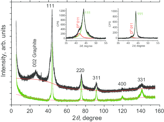
DP 0-0.05 分数的多晶金刚石颗粒(黑色曲线)和通过烧结获得的 D19 纳米金刚石(绿色曲线)的粉末 XRD 谱。插图:来自平面 (111) 的最强烈反射与中心在 41.5° (D H ) 的两条(红色和绿色)洛伦兹曲线的拟合 011) 和 43.8 o (D c 111) 烧结前(左插图)和烧结后(右插图)的样品
为了进一步了解复杂的前体 DP 0-0.05 金刚石多晶结构,我们使用了高分辨率透射电子显微镜(HRTEM,JEOL JEM-2100F,配备 CEOS Cs 校正器,信州大学)。 HRTEM 在 80 kV 下运行以最大限度地减少辐射损伤。 HRTEM 图像(图 4)显示多晶由紧密结合的立方纳米金刚石微晶组成,特征为 1.93 Å d - 间隔条纹。图 4a 中成像的多晶由大小为 5 到 12 nm 的微晶组成,具有不同的取向,用不同的颜色标记。此外,HRTEM 表明构成 DP 0-0.05 粉末的单个多晶的尺寸分布广泛,在 5-50 nm 范围内。 HRTEM 图像没有显示任何六边形金刚石纳米相(如 lonsdaleite)的痕迹。然而,我们观察到许多短孪晶边界(图 4c、d),其中一些显示出具有手风琴形状的褶皱晶格平面,如图 4d 所示。这些观察结果表明,前面讨论的 111 XRD 峰肩(图 3)最有可能是由于与多个孪晶相关晶界相关的堆垛层错,而不是六方金刚石相的存在 [16]。
<图片>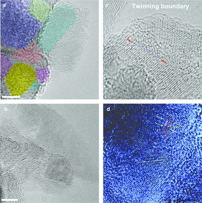
从 DP 0–0.05 粉末中提取的选定立方金刚石多晶的高分辨率 TEM 图像 (a , b ) 和简单孪晶边界的典型图像,长度为几纳米,偶尔在样品中发现 (c , d )。面板 (a , b ):比例尺——4 纳米。不同的微晶在 (a )。面板中的箭头 (c ) 和 (d ) 标记选定的清晰可辨的孪生边界
使用有机元素分析系统(JM10,J-Science Lab Co., Ltd,Kyoto,Japan)通过 Pregl-Dumas 方法分析 DP 0-0.05 的元素组成,其中样品在 1007°C 下燃烧氧气流量(30 毫升/分钟)。氧分数由天平确定。分析结果,以wt%计,为:C—90.45,N—2.47,H—0.76,O—6.32。相对较大的氮浓度意味着几乎所有的氮都以聚集形式存在于多晶内,可能以 A 中心(NN-二聚体)的形式存在。 X 射线荧光进一步分析显示 DP 0-0.05 中存在其他微量元素:Fe (~ 300 ppm)、Cu (35 ppm)、Si (120 ppm)、Cr (~ 150 ppm)、Ca (~ 45 ppm)、Mn (45 ppm)、P (30 ppm)、Al (18 ppm)、Ti (13 ppm)、Mg (6 ppm)、Ni (2 ppm)、Zn (2 ppm)、Co (1 ppm) .
用于后续磁共振研究的 DP 0-0.05 样品在沸腾的盐酸中额外处理,以将铁磁性金属(主要是铁和铬)的存在减少到 ~ 10 ppm 的水平。
烧结金刚石的结构表征
我们还对通过烧结 DP 0-0.05 获得的样品 D19 进行了类似的表征。通过与 DP 0-0.05 粉末相同的方法获得 D19 XRD 图。发现仅显示了立方金刚石相的五个洛伦兹峰特征(图 3,绿线),对应于 111、220、311、400 和 331 平面。没有证据表明前体材料中存在石墨相。 111 峰的不对称性也大大降低(图 3,右插图)。这表明堆垛层错的相应显着减少。此外,L 发现 CSR 相干长度为 10.8 nm,表明在烧结过程中金刚石纳米微晶增大。考虑到这些观察结果,我们假设石墨和非立方金刚石相在烧结过程中转化为立方金刚石相。这可能是由于这些相的溶解,随后在多晶微晶之间的间隙空间内生长了立方金刚石相。先前已在爆炸纳米金刚石中观察到这样的过程[14]。
D19 样品的光学和扫描电子显微镜图像分别显示在图 5a、b 中。在这里,我们看到了大小从 ~ 0.3 到 ~ 5 微米的任意形状的颗粒。它们实际上是通过共价键或弱范德华键结合在一起的小得多的金刚石微晶的致密亚微米和非常松散的微米级聚集体。这种键通常由相邻金刚石颗粒的表面官能团的相互作用产生。通过透射电子显微镜可以看到构成这些松散聚集体的单个金刚石颗粒。尺寸约为 ~ 100 nm 的 D19 金刚石微晶的 TEM 图像如图 5c 所示。该图像是使用 JEOL JEM-2100F 透射电子显微镜(Hosei University)在 200 kV 的加速电压下拍摄的。将样品固定在无碳基底的铜网上。
<图片>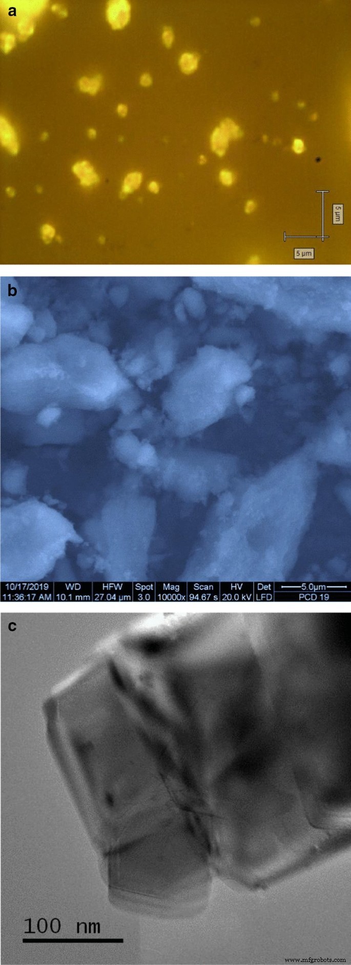
光学 (a ), 扫描电子显微镜 (b ) 和透射电子显微镜 (c ) 合成的 D19 金刚石颗粒的图像。光学图像是用 100 倍显微物镜拍摄的。用于拍摄电子 SEM 图像的相应参数显示在面板底部 (b )
预烧结和后烧结纳米金刚石缺陷含量的分析方法
两种钻石样品均通过 EPR、拉曼和荧光光谱法进行分析。使用 EPR 光谱仪(JES-FA 300,JEOL,日本)在室温、9.444 GHz 的微波频率下记录 EPR 光谱。将质量为 20 毫克的粉末引入直径为 4 毫米的石英 EPR 管中。管中粉末柱的高度不超过 10 毫米。管的开口端密封防潮。
具有 g 的 EPR 光谱 - g 范围内的因素 =4.00–4.30 用P的微波功率记录 MW =10 mW,磁场调制幅度A m =1 mT 和频率 ν =100 kHz,放大器增益 G ≈ 10 3 , 和 N =16 个信号累积周期。选择这些参数以获得最佳信噪比。时间常数为 0.03 s,130-200 mT 间隔内磁场扫描的总记录时间为 120 s。具有 g 的 EPR 光谱 -因素 g ≈ 2 记录在 327 到 347 mT 区间,微波功率为 P MW =0.03 mW,磁场调制幅度A m =0.035 mT,放大器增益 G ≈ 10 2 , 和 N =4 个信号累积周期。请注意,作为一项规则,对于广泛的主要 EPR 信号 (g ≈ 2) 线宽> 0.5 mT,峰峰值 EPR 信号强度 (I pp) 遵循 MW 功率依赖性 I pp ~ (P MW) 1/2 直到 P MW ≈ 100 mW。另一方面,对于窄 EPR 信号(线宽 <0.15 mT 在低功率下),I pp 在 P 处饱和 MW> 0.05 mW,并且在较高值 (> 4 mW) 时具有强烈的形状畸变。对于多晶前驱体和随后的烧结金刚石均观察到这种饱和趋势。
我们使用微型拉曼光谱仪(“inVia”,Renishaw,UK),结合使用 50× 物镜(NA =0.78)和 CCD 的光学显微镜(Leica,德国)获得了光致发光 (PL) 和拉曼光谱检测器冷却至 -70°C,背散射几何。以 ~ 2 cm –1 的光谱分辨率记录光谱 .我们使用了 488 nm 和 457 nm 波长的氩离子激光器的两条激光线,强度小于 20 W cm -2 在样品的焦点上。我们以 StreamLine™ Plus(英国雷尼绍)模式记录光谱图像,与标准聚焦在微米大小的圆上相比,由于聚焦在 2 × 30 微米的条纹上,因此在样品平面中使用较低的激发激光强度。该策略通过环境大气中的过热和氧化来限制激光诱导的样品损坏和局部气相蚀刻。该技术的更多细节以及在直径为 2 毫米的圆柱体中压制金刚石粉末的详细信息之前已经描述过 [19]。
使用 100 倍物镜的共聚焦宽视场落射荧光显微镜获得分离的 D19 颗粒的荧光图像。通过旋涂,将颗粒从稀释的 D19 粉末水基悬浮液的上清液部分沉积在玻璃盖玻片上。盖玻片在氧等离子体中进行了初步处理,以避免残留有机物的寄生荧光,并促进 D19 颗粒更好地附着在盖玻片上。用 488 nm 激光(激发功率 ≈ 40 mW)激发荧光,并用 525/40 干涉滤光器收集。使用特别冷却的二维阵列 CCD 检测器(相机温度 =− 79.9°C)记录图像。图像(尺寸 ~ 80 × 80微米,80.00纳米/像素)以60毫秒的曝光时间记录。灰度托盘用于图像呈现。使用斐济软件分析图像。
结果
烧结前后多晶和金刚石微晶的EPR
DP 0-0.05 多晶金刚石粉末在半磁场范围和高场范围内的 EPR 光谱如图 6 所示。在这些不同范围内记录的 EPR 光谱是在高和低微波下测量的权力P MW =10 mW 和 P MW =0.03 mW。这里的高场区通常选择在与主微波感应触发器 ΔM 相关的吸收线附近 s =1 次自旋 S =½,而专门选择扩展的半场范围来搜索来自 ΔM 的信号 s =2 可能的三元组 S 的转换 =1 个中心。半场 EPR 光谱强度非常低,表明存在三重态 NV − 中心(带有 g 的信号 =4.27 在 H res =158 mT [10, 16]) 和三重态多空位(带有 g 的信号 =4.00 在 H res =168 mT [16]) 在多晶金刚石前体中。这两种缺陷类型都以非常低的浓度 (<1 ppm) 存在;因此,有必要使用高微波功率来检测此类稀有中心。此外,在高场域中,我们还观察到自旋半中心 (g =2.0027 在 H res =337 mT [10, 16, 21]),但具有广泛的 (ΔH pp =0.47 mT),没有任何精细结构的单一洛伦兹导数形状 [16]。鉴于这些自旋来自独立中心的假设,这种广泛而强烈的信号可以暂时归因于 C-C 悬空键自旋和交换耦合顺磁性氮自旋与未解析的超精细结构 (HFS)。 脚注 2 我们用自旋 S 估计了所有顺磁性物质的浓度 =1/2 为 ~ 4 × 10 19 spin/g (800 ppm),比之前报道的 5 nm 爆炸纳米金刚石 [22] 的值小 ~ 1.5 倍。
<图片>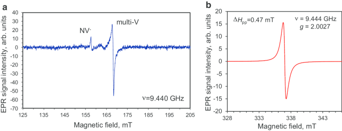
在半磁场范围 (a ) 以及在 g 处具有强信号的单线态共振磁场周围 -因子 g ≈ 2.0027 (b )。微波功率P MW:10 毫瓦 (a ) 和 0.03 mW (b )。微波频率 ν =9.44 GHz。两个光谱都记录在远离饱和的区域
图 7a 显示了 D19 样品在极低 (P MW =1 μW) 和非常高 (200 mW) 的微波功率,即 分别在远低于饱和或处于饱和状态(如展宽所证明)。 P 的频谱 与前体颗粒相比,MW =1 Wμ 的中心线具有更窄的线宽 0.14 mT。图 7b(曲线 1)显示了双重积分的低微波功率 EPR 信号。该信号可以分解为:与最丰富的 S 相关的宽 (FWHM ≈ 1.7 mT) 洛伦兹形信号(图 7b,曲线 2) =1/2 物种(局部密度高并组织成自旋簇)和一条非常窄的中心线,两条对称卫星线相隔 ~ 6 mT(图 7b,曲线 3)。两条卫星线相对于中心线的综合强度比分别为 0.90 和 1.09。因此,它们在 ± 10% 的实验测量精度内具有相同的积分强度。卫星线与中性顺磁置换氮( 14 N, S =1/2, I =1),称为 P1 中心 [23, 24]。在前体多晶纳米金刚石中没有观察到 P1 中心,但在烧结后的金刚石中可以清楚地检测到 P1 中心。先前的工作表明,这种与 P1 中心相关的特征性三重态 HFS 结构仅出现在尺寸超过 50-80 纳米的粗金刚石晶体中 [25]。此外,已证明在乙醇存在下烧结爆炸纳米金刚石可促进基于金刚石再结晶和新金刚石相生长的微晶增大 [26]。因此,当前的 EPR 数据与此处发生的类似放大一致,从尺寸 ~ 7-10 纳米的多晶颗粒的单个微晶到单个尺寸 ~ 40-50 纳米的新微晶。 脚注 3
<图片>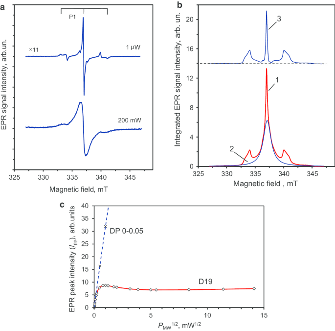
D19 金刚石晶体在低和高微波功率下的主要一阶导数 EPR 信号 (a ),将整合的 EPR 信号分解为与两组自旋相关的分量 (b ),以及该 EPR 信号的峰值强度相对于微波功率平方根在高达 200 mW 范围内的相应饱和趋势 (c )。 P1 中心(取代氮)的 EPR 信号的三重 HFS 结构在 (a )。在 (b ):曲线 3,具有三重结构,对应于仅 P1 中心的 EPR 谱。在 (c ):虚线是I pp 与 (P MW) 1/2 DP 0-0.05 多晶的依赖性供参考。 P 的四个实验点 MW =0.5, 1, 2, 4 mW 用于其绘图(此处未显示其中两个)。微波频率 ν =9.44 GHz
这一假设不仅被窄 EPR 信号的观察所证实 脚注 4 (g =2.0024) 具有 HFS 特征的 P1 中心 [26],但也通过检测 I P 以上的 pp 饱和度 对于 D19 样品,MW =0.7 mW。对于前驱体多晶纳米金刚石 DP 0-0.05,即使在高微波功率(P MW =20 毫瓦)。权力依赖I pp ~ (P MW) 1/2 在整个微波功率范围内保持良好 (P MW =0–20 mW)。 我 pp ~ (P MW) 1/2 DP 0-0.05 样品的依赖性在图 7c 中由虚线显示,微波功率高达 ~ 16 mW。这种没有饱和的线性相关性是由于多晶纳米金刚石中顺磁中心的高浓度以及非常短的自旋-晶格和自旋-自旋弛豫时间造成的。 D19样品g的饱和行为 =2.0024 EPR 信号也在图 7c 中显示在 0-200 mW 范围内。 脚注 5 我们观察到一个 I pp ~ (P MW) 1/2 仅适用于低于 ~ 15 Wμ 的微波功率。在这种情况下,I pp 表明在低于 1 mW 的范围内饱和,并在 ~ 1 mW 处达到最大值。 我 pp 然后在 1-25 mW 范围内大幅下降,然后再次缓慢增加到最大使用功率 (200 mW)。 I 中存在这种饱和趋势 pp (P MW),也低于 P MW =1 mW,是 P1 中心的特征,具有相对较大的自旋-自旋和自旋-晶格弛豫时间,远离其他缺陷和粒子边缘 [27]。对于尺寸超过 60-80 nm 的 Ib 型 HPHT 纳米金刚石中小于 200 ppm 的 P1 中心浓度,满足这些条件。然而,仅从 EPR 的角度来看,单个 D19 金刚石微晶(基本颗粒)的实际平均尺寸是一个悬而未决的问题。通过将 D19 的实际 EPR 光谱与平均尺寸从 18 到 390 nm 不等的研磨 Ib HPHT 钻石的一系列粉末 EPR 光谱进行比较,可以粗略地解决这个问题 [28]。跟随参考。 [28] 在这些 EPR 光谱发表的地方,与置换氮相关的 P1 HFS 特征在平均尺寸 ≤ 30 纳米的粉末金刚石中完全不存在,但仍存在于中等尺寸(85-130 纳米)的样品中。该比较表明合成的 D19 金刚石微晶的平均尺寸在 10,030 ± nm 的范围内。这种估计与图 5c 所示的 TEM 图像中观察到的代表性尺寸非常吻合。值得注意的是,在 P 的高功率下记录的 D19 的 EPR 谱 MW =200 mW(图 7a)显示 P1 信号的 HFS 结构缺乏定义。 The broad central line suggests the presence, at the nanoscale, of dense clusters of paramagnetic spin-half that strongly couple to each other.
Altogether, the decrease in the linewidth of the main EPR signal (g = 2.0024), the appearance of well-defined HFS characteristics in the P1 centre spectrum after sintering, and the I pp saturation for P MW > 0.7 mW (Fig. 7c) are suggestive of an increase in size by up to one order of magnitude (crystal size > 50 nm). It also indicates a better crystallinity of the nanodiamond in the D19 sample. From van Wyk measurements [29], a smaller amount of paramagnetic defects (< 200 ppm) are expected, based on the narrow linewidth (0.14 mT) of the g = 2.0024 main paramagnetic signal in the D19 sample.
Fluorescence and Raman Scattering of Diamond Crystals
The photoluminescence (PL) spectrum of the DP 0–0.05 precursor together with the PL spectra of some much coarser fractions of polycrystalline diamond particles (DP 0–0.2 and DP 0–0.35) produced by Microdiamant TM is shown in Fig. 8. The spectrum of DP 0–0.05 under the 488 nm excitation wavelength has two features of note:the prominent narrow PL line at 738 nm, associated with the zero-phonon line of negatively charged SiV − centres, and a broad spectrum background with PL bands centred at 525, 600, 660 and 740 nm, associated with various light-emitting centres in diamond, including NV centres. For polycrystals with mean size 25 nm (DP 0–0.05), the intensities of these bands are smaller than that for polycrystals with mean sizes of 100 and 175 nm (DP 0–0.2 and DP 0–0.35, respectively). A more detailed analysis of the PL spectra of polycrystalline DP 0–0.05 particles has been previously undertaken [19].

PL spectra of various submicron fractions of Microdiamant™ polycrystalline diamond particles:blue—DP 0–0.05 (mean size 25 nm), green—DP 0–0.2 (mean size 100 nm), red—DP 0–0.35 (mean size 175 nm). Excitation wavelength λ = 488 nm. The prominent peak at 738 nm marked by the vertical dashed line is the zero-phonon line of negatively charged SiV − centres, which can be observed in all polycrystalline diamond fractions. For better comparison, the spectra are specially normalized for PL intensity at λ = 590 nm. Normalising coefficients are indicated in the figure
Figure 9a shows the PL spectrum of sintered diamond sample D19 (blue curve) at room temperature (RT) together with the PL spectrum of the DP 0–0.05 precursor (red curve). The D19 spectrum displays a green fluorescence characteristic, with a sharp maximum at 525 nm, and a subsequent decrease at larger wavelengths. Note that the single-phonon, sharp Raman line of diamond, which is expected at 522 nm, was too weak to be detected on the ascending slope of the PL signal under 488 nm excitation wavelength. Footnote 6 As previously reported [9, 30], such spectra—with a continuous higher wavelength band of “triangular” shape—are characteristic of optical emission from NVN centres (also known as H3 centres) in submicron (< 140 nm) diamonds at RT. In the PL spectrum of sample D19, at least four broad bands (“bumps”) centred at 538, 569, 601 and 710 nm can be additionally distinguished. We do not believe that they are related to phonon sidebands of the NVN (H3) centres. The origin of the 525 nm sharp peak and “bumps” is still unclear, but it is probably due to an impurity-related complex; the precursor material contains a large number of residual contaminants as mentioned before (see “Structural Characterisation of the Materials Before and After the Sintering” section), some of which are present at significant concentrations (~ 100 ppm). The zero-phonon emission line of NVN at ~ 503 nm wavelength is barely detectable and cannot be distinguished from the two small shoulders (at 500 and 505 nm) in the same region. By comparing the D19 and DP 0–0.05 spectra (Fig. 9a), one can see that they superimpose well for λ > 750 nm. However, the spectra differ significantly in the 480–650 nm range due to the appearance after sintering of NVN centres, which were not present in the precursor material. In order to verify our interpretation of the main optical emission of D19 (in the range 500–650 nm) as originating from NVN centres, we compared the PL spectrum of D19 with the PL spectra of two reference samples (HPHT diamonds, Columbus NanoWorks Inc., US) of two very different sizes and both known to contain NVNs (Fig. 9b). The D19 PL spectrum (dashed line) coincides very well with those of the PL spectra of the HPHT microdiamonds containing NVNs. The emission spectrum of the 100-µm sized reference sample shows a sharp single-phonon diamond Raman line (487.4 nm) and the zero-phonon line (504 nm) of NVN under 457 nm laser excitation at room temperature (Fig. 9b, violet spectrum). The 150-nm sized HPHT nanodiamonds were excited at 488 nm, and it displayed a very similar global photoluminescence spectrum shape as that of the 100-µm sized sample, with a Raman single-phonon line at 522 nm. However, it did not exhibit the NVN zero-phonon line, behaving in that sense exactly like the D19 sample. The “bumps” present in the D19 sample spectrum are absent from both reference PL spectra, indicating that these features are not related to the NVN emission.

PL spectrum of submicron powder D19 sample at T = 293 K (blue line) compared with that of its DP 0–0.05 polycrystalline precursor (red line) under the same conditions with laser excitation at λ = 488 nm (a ), emission spectra, under 457 nm and 488 nm excitation, of two reference synthetic HPHT samples (size ~ 100 μm and < 150 nm) containing NVN centres (b ) and the Raman spectrum of D19 sample recorded using the 457 nm excitation laser radiation (c )。 Arrows in (b ):lines at 487.4 nm and 522 nm are single-phonon diamond Raman lines at 457 nm and 488 nm excitation, respectively, and the line at 504 nm is the ZPL of the NVN centres. In (b):dashed line—PL spectrum of D19 at λ = 488 nm excitation (for comparison). In (c ):the diamond Raman line is centred at 1331.4 cm −1 . δ = 7.3 cm −1 is a FWHM of diamond Raman line having the Lorentzian shape
We also measured Raman scattering from D19, in the range 1000–1600 cm −1 , under excitation by 457 nm laser radiation. Figure 9c displays the Raman spectrum, corrected to remove the autofluorescence background. The spectrum consists primarily of a narrow characteristic diamond Raman line centred at 1331.4 cm −1 and an exceptionally broad (width ≈ 100 cm −1 ) band centred at 1450 cm −1 . The latter could be due to non-diamond amorphous carbon phase and/or some transpolyacetylene (TPA) species located at diamond crystals surface [1,2,3]. A further, ill-defined, band at ~ 1090 cm −1 of lower intensity is probably related to TPA species. The broad band at ~ 1450–1480 cm −1 could also be related to multivacancy chains in the diamond lattice and sp 2 - rehybridisation within these chains [6]. Footnote 7 Furthermore, we did not observe the characteristic G-band (centred at 1570–1590 cm −1 ) associated with an sp 2 graphitic nanophase. These observations are indicative that the diamond sample D19 being graphite free, which is also in agreement with its white colour under daylight illumination.
Moreover, the width of the Raman diamond line (7.3 cm −1 ) in the D19 sample is smaller than that for the DP 0–0.05 polycrystalline particles (10.6 cm −1 )。 Table 1 contains Raman diamond line data for bead-milled synthetic Ib HPHT diamonds with mean size varying from 25 to 1000 nm (Microdiamant AG, Switzerland). The linewidth decreases from 9.12 to 5.24 cm −1 with increasing size. This can be explained by the lower prevalence of structural defects in larger crystals. Using data as a calibration curve to infer the crystal size from the diamond Raman linewidth of δ ≈ 7.3 cm −1 yields an estimation for the D19 crystal size of ~ 80 nm. This value coincides reasonably with the estimation in “EPR of Polycrystals and Diamond Crystallites Before and After the Sintering” section on the basis of EPR data. Moreover, this value is very similar to our previous published results where diamonds were obtained by HPHT sintering of 5-nm DND in the presence of ethanol [31]. However, the precursor material used for sintered DND and the one used in this work using the smallest (~ 25 nm) fraction of milled Du Pont shock-wave polycrystalline diamonds are considerably different from the viewpoint of crystal types and elementary crystallite sizes. This obtained size is about 8 times larger than the coherent scattering region length of L CSR ≈ 11 nm extracted from XRD earlier, but it is consistent with crystallite having a low density of structural defects, in agreement with the EPR studies.
We also studied the fluorescence from very fine individual D19 particles. For this purpose, the supernatant fraction of diluted and ultrasonicated water suspension of D19 particles obtained after centrifugation at 4500 × g for a 30 min was used. Coarse particles and large loose aggregates with size exceeding ~ 0.2–0.3 micron were absent in such supernatant. Fine D19 particles were spin-coated onto a thin glass coverslip from the diluted supernatant of D19 particles. A typical image of fine fluorescent D19 particles is shown in Fig. 10a in greyscale (mono 14-bit images). It consists of many spots with different brightness. Some spots, such as that marked by the yellow circle, have sizes close to the diffraction limit. The intensity profile of this spot has a Gaussian shape in its central core and a FWHM of about 5–6 pixel corresponding to ~ 440 nm (Fig. 10b). Such spots come from at least quarter-micron particles and particles of smaller size. A greater number of brighter spots correspond to the larger reassembled aggregates of D19 particles having more NVN colour centres and hence the overall emission intensity increasing.

Wide-field fluorescent image of isolated D19 particles obtained by confocal epifluorescence microscopy (a ), and the intensity profile of the selected nanoparticle marked by the yellow circle (b )。 Image size: ~ 80 × 80 mμ. One pixel corresponds to 80 nm
Discussion
We showed that under HPHT conditions, and in the presence of ethanol, we can convert polycrystalline diamond particles (composed of tightly cemented nanometre-sized cubic diamond crystallites separated by a non-cubic diamond phase) into larger cubic diamond crystallites. The process probably occurs through recrystallisation of the cubic diamond phase and transformation of non-cubic diamond phases including multiple twin boundaries into diamond. During this process, vacancies appear and can form NVN complexes with nitrogen atom pairs. These complexes have a characteristic photoluminescence in the green. While the EPR spectra of the precursor polycrystalline diamonds show NV − triplet centres, triplet multivacancies, and SiV − centres, none of these were present after the sintering. The disappearance of NV − centres and multivacancies has previously been observed [31] after sintering detonation nanodiamonds at HPHT conditions (P = 7 GPa and T ≥ 1350 °C) with ethanol. Footnote 8 The presence of multivacancies is a characteristic feature of damaged diamond lattices, with defects mainly located in a thin layer of ~ 2 nm at the surface. The absence of the paramagnetic triplet and SiV colour centres is strong evidence that substantial recrystallisation took place, accompanied with the appearance of new defect types (NVN). The saturation trend of the substitutional nitrogen (P1 centre) EPR signal with increasing microwave power indicates long spin–spin and spin–lattice relaxation times. These are signatures of improvement of the quality of diamond crystal lattice after sintering. We can assume that during HPHT sintering, vacancies from empty spaces within or between polycrystals join with A-centres to form the new NVN entities.
结论
Sintering of diamond polycrystals, with size varying from 3 to 50 nm, in the presence of ethanol, lead to the substantial enlargement of elementary diamond nanocrystals and improved their crystalline quality. During this process, SiV − and NV − colour centres present in the precursor nanodiamond disappeared, while the EPR signature of P1 substitutional nitrogen paramagnetic centres appeared. We also observed the green photoluminescence of NVN colour centres. The comparison of the FWHM of diamond Raman line (~ 1332 cm −1 ) of the synthesised selected microcrystals under study with those of a series of reference samples revealed that the mean size of diamond crystals after sintering is approximately 80 nm. The analysis of the EPR spectrum dependence upon microwave power demonstrated the good crystalline quality of the synthesised sintered diamond with a concentration of P1 centres smaller than 200 ppm. Hence, our technique of HPHT sintering is a strong alternative to conventional high-energy particle beam irradiation [9] to form NVN centres in nanodiamond. It can be used to produce purely “green” fluorescing nanodiamonds with no (or very limited) crosstalk with the “red” fluorescing nanodiamonds (containing NV 0 and NV − centres), as required in biolabelling for cathodoluminescence integrated correlation electron-light microscopy [32].
数据和材料的可用性
The data underpinning this manuscript is available from the corresponding author on request.
Notes
- 1.
The apparatus response function of the XRD diffractometer was determined from a LaB6 reference sample.
- 2.
One mechanism explaining the lack of HFS in the EPR signal of paramagnetic nitrogen in size < 50 nm diamond nanoparticles is described in detail elsewhere [21]. Alternative mechanisms are also not excluded [33, 34].
- 3.
X-ray diffraction CSR size is ~ 4 times smaller in this case.
- 4.
This narrow EPR signal is slightly asymmetrical and consists of at least two components related to P1 centres and to defects having C–C dangling bond spins S = 1/2. The intensity of the second component represents at least 30% of the intensity of the main peak.
- 5.
Here we assume the sequence of untreated first-derivative experimental EPR spectra measured at different P MW, two of which are shown in Fig. 7a.
- 6.
However, the Raman line was detected at 457 nm excitation.
- 7.
The Raman band centred at ~ 1480 cm −1 was found for HPHT diamonds grown with magnesium-based catalysts [6]. Such diamond crystals may contain SiV and GeV colour centres.
- 8.
Instead of a multivacancy g = 4.00 singlet EPR signal, a new EPR signal with a quintet hyperfine structure related to N⋯N pairs separated by no more than 0.7 nm was observed in this case.
缩写
- NV − :
-
氮空位
- NVN:
-
Nitrogen-vacancy-nitrogen
- HPHT:
-
High-pressure, high-temperature
- DND:
-
Detonation nanodiamond
- EPR:
-
Electron paramagnetic resonance
- FWHM:
-
半高全宽
- XRD:
-
X射线衍射
- LCSR:
-
Coherent scattering region length
- HRTEM:
-
高分辨透射电子显微镜
- PL:
-
光致发光
- MW:
-
Microwave
- HFS:
-
Hyper-fine structure
- RT:
-
室温
纳米材料