

InGaAs/InAlAs SAGCM 雪崩光电二极管的理论研究
摘要
在本文中,我们详细介绍了 InGaAs/InAlAs 单独的吸收、分级、电荷和倍增雪崩光电二极管 (SAGCM APD),并建立了 APD 的理论模型。通过理论分析和二维(2D)模拟,充分了解电荷层和隧道效应对 APD 的影响。电荷层的设计(包括掺杂水平和厚度)可以通过我们针对不同倍增厚度的预测模型进行计算。我们发现随着电荷层厚度的增加,电荷层中合适的掺杂水平范围减小。与较薄的电荷层相比,APD 的性能因较厚电荷层中掺杂浓度的几个百分比偏差而显着变化。此外,生成率 (G btt )计算带间隧道,分析隧道效应对雪崩场的影响。我们确认雪崩场和倍增因子 (M n ) 在乘法中会因隧道效应而减少。理论模型和分析基于InGaAs/InAlAs APD;但是,它们也适用于其他 APD 材料系统。
背景
In0.53Ga0.47As(以下简称InGaAs)雪崩光电二极管(APD)是短波红外探测中最重要的光电探测器。它们在光纤通信、侦察应用和遥感等传统领域具有重要意义。 InP和In0.52Al0.48As(以下简称InAlAs)具有与InGaAs相同的晶格间距和很好的雪崩击穿特性;因此,它们是传统应用中合适的 InGaAs APD 倍增层材料。近年来,由于单光子检测在量子密钥分配[1]、时间分辨光谱[2]、光学VLSI电路检测[3]和3D激光测距[4]等方面的快速发展,APDs作为关键这些应用中的组件越来越受到关注 [5, 6]。佩莱格里尼等人。描述了平面几何 InGaAs/InP 器件的设计、制造和性能,这些器件是为单光子检测而开发的,在 1550 nm (200 K) [7] 处的单光子检测效率 (SPDE) 为 10%。托西等人。介绍了具有高 SPDE(30%,225 K)、低噪声和低时序抖动的新型 InGaAs/InP 单光子雪崩光电二极管 (SPAD) 的设计标准 [8]。在仿真方面,建立了基于实验数据的器件模型来预测 [9] 中 InGaAsP/InP SPAD 的暗计数率(DCR)和 SPDE,以及可以评估 InGaAs 诱饵态量子密钥分配性能的集成仿真平台/InP SPAD 内置于 [10]。阿瑟比等人。介绍了带有定制 SPAD 模拟器的 InGaAs/InP 单光子 APD 的设计标准 [11]。对于 InGaAs/InAlAs APD,证明了台面结构 SPAD InGaAs/InAlAs 可实现 21% (260 K) 的 SPDE;然而,观察到高 DCR 并归因于过大的隧道电流 [12]。然后,[13] 在 InGaAs/InAlAs APD 中使用厚的 InAlAs 雪崩层来提高 SPDE (26%, 210 K) 并降低 DCR (1 × 10 8 赫兹)。在模拟InAlAs基APDs时,建立了基于Monte Carlo方法的器件模型,研究了[14]中InGaAs/InAlAs APDs的基本特性,以及电荷层和倍增层对穿通电压和击穿电压的影响在[15]中用稳态二维数值模拟研究了电压。
与InAlAs基APDs相比,InP基APDs的研究在理论和仿真上更加全面和深入。然而,基于 InAlAs 的 APD 越来越多地用于代替 InP,因为它具有更大的带隙,可以改善 APD 和 SPAD 的击穿特性 [16]。与 InP 相比,InAlAs 中电子 (α) 与空穴 (β) 的电离系数比更大,因此,它具有低过量噪声因子和高增益带宽积。此外,InAlAs 的击穿概率随过偏比大幅增加,使得 InAlAs SPAD 具有较低的 DCR [17]。从先前的研究中获得了关于基于 InAlAs 的 APD 的一些重要特性和结论,例如在具有厚和薄雪崩区域的 InAlAs 结构中可以实现低过量噪声 [18]。吸收(InGaAs)中的隧穿阈值电场为1.8 × 10 5 V/cm,隧道电流成为高场暗电流的主要成分[14]。垂直照明结构具有更大的光学容差,但它在载流子传输时间和响应率之间有更严重的权衡[19]。此外,[20,21,22] 还研究了理论模型、结构(厚度和掺杂)、电场和其他基于 InAlAs 的 APD 参数。然而,这些研究只关注常见的 APD 结构参数的影响,如吸收层厚度、倍增厚度和电荷层掺杂水平。 InAlAs基APD的结构参数与性能之间的关系尚未完全理解和优化。
在本文中,基于 InGaAs/InAlAs 垂直结构的用于 1.55-μm 波长检测的理论研究和数值模拟分析进行了研究。我们建立了一个理论模型来研究结构参数对器件的影响以及 APD 中各层的详细关系。对不同倍增层厚度的电荷层设计、厚度对电荷层掺杂水平的影响以及倍增层中隧道效应对雪崩场的影响进行了分析和模拟。
方法
在本节中,建立了器件参数与器件内电场分布的数学关系,用于分析电荷层和隧穿效应。同时建立了包括仿真结构、材料参数和基本物理模型在内的仿真模型。理论分析模型和仿真模型基于SAGCM InGaAs/InAlAs APD垂直结构。
电荷层的理论模型与分析
器件参数,如掺杂水平、厚度、材料和结构,被用来建立数学模型来计算 APD 中的电场分布。包括泊松方程、耗尽层模型和半导体器件PN结模型在内的基本物理理论可以在[23]和[24]的第1、2和4章中找到。结倍增因子方程可以在[25]中找到,半导体的材料参数来自[26]。该模型采用泊松方程、隧道电流密度方程、耗尽层模型、结理论模型和雪崩增益局部模型。包含基本结构参数(材料、厚度、掺杂和介电常数)的 APD 简化数学坐标系如图 1 所示。它是一种忽略渐变层的简化 SACM APD 结构。接触层、电荷层和倍增层的材料为InAlAs,吸收层为InGaAs。层的连接处由 X 分隔 n , 0, X 米 , X c , 和 X 一 和 X p 由 x 协调。掺杂水平用N表示 0 , N 1 , N 2 , N 3 , 和 N 4 ,层厚用w表示 0 , w 1 , w 2 , w 3 , 和 w 4 ,介电常数用ε表示 s0 , ε s1 , ε s2 , ε s3 , 和 ε s4 分别为接触A、倍增、电荷、吸收和接触B。
<图片>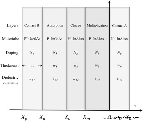
SACM InGaAs/InAlAs APD 的简化数学坐标系。介绍用于构建理论模型的 APD 的简化结构。包含基本结构参数(材料、厚度、掺杂和介电常数)的APD简化数学坐标系
方程1是泊松方程,可以利用电荷密度ρ求解电势分布 .在这个等式中,ρ 等于掺杂离子N 在耗尽层模型中,w 等于耗尽层的厚度,并且ε 是材料的介电常数。在普通PN结电场分布模型中,ρ 是一个取决于耗尽层厚度的变量 w 和掺杂离子N .在这个模型中,它在考虑隧道效应后发生了变化。然而,在考虑隧道效应之前,我们首先使用通用方法构建了电场分布。
$$ \frac{d\xi}{d x}=\frac{\rho }{\varepsilon }=\frac{q\times N}{\varepsilon } $$ (1)通过用器件参数求解泊松方程,得到最大电场的数学表达式。该表达式由公式 2 和 3 中所示的耗尽层中的穿透厚度变化决定。在该表达式中,包括掺杂水平 (N ), 耗尽层的厚度 (w ) 和介电常数 (ε) 不同层的数量可以在图 1 中找到。
$$ {\xi}_{\max (w)}={\sum}_{k=1}^4\left(-\frac{q\times {N}_k\times {w}_k}{\ varepsilon_{sk}}\right) $$ (2) $$ {\xi}_{\max (w)}=\frac{q\times {N}_0\times {w}_0}{\varepsilon_{s0 }} $$ (3)然后,可以使用公式 4 和 5 导出所有点的电场分布。边界条件忽略内置电位 V 公式 6 中的 br;因此,可以计算出耗尽层厚度与偏置电压之间的数学关系。
$$ {\xi}_{\left(x,w\right)}={\xi}_{\max (w)}+{\sum}_{k=1}^4\left(\frac{ q\times {N}_k\times \left|x\right|}{\varepsilon_{sk}}\right)\left({X}_p从模型中,一旦耗尽层的边界到达接触区,就可以用公式 7-11 来分析每一层的电场。在实际的 APD 中,吸收层和倍增层无意中掺杂在本征层中。 N 3 和 N 1 小于 N 2 .因此,公式9近似等于公式12。这就是电荷层可以控制器件中电场分布的原因。
$$ {\displaystyle \begin{array}{l}\xi \left(x,{V}_{\mathrm{bias}}\right)={\xi}_{\max \left({V}_ {\mathrm{bias}}\right)}+\frac{q\times {N}_1\times {w}_1}{\varepsilon_{s1}}+\frac{q\times {N}_2\times { w}_2}{\varepsilon_{s2}}+\frac{q\times {N}_3\times \left|x-{X}_c\right|}{\varepsilon_{s3}}\\ {}\kern4em \approx {\xi}_{\max \left({V}_{\mathrm{bias}}\right)}+\frac{q\times {N}_2\times {w}_2}{\varepsilon_{ s2}}\left({X}_{\mathrm{c}}\ge x\ge {X}_a\right)\end{array}} $$ (12)在公式 8 中,乘积和吸收之间的电场差由 N 的乘积确定 2 和 w 2 . N 2 是电荷层的掺杂水平,w 2 是电荷层厚度。为了在 InGaAs/InAlAs APD 中获得合适的电场分布,吸收层 (InGaAs) 中的电场应在 50-180 kV/cm 的区间值内,以确保光生载流子有足够的速度并避免隧道效应在吸收层 [10]。也就是说,倍增中的雪崩场在电荷层的吸收中应降低到 50-180 kV/cm。因此,我们可以使用公式 8 来找到电荷层的最佳计算掺杂水平和厚度。当倍增层为 200 nm(雪崩场 E 在乘法中是6.7 × 10 5 V/cm 而倍增层为 200 nm [27]);电荷层中的掺杂水平和厚度的计算值与图2中[28,29,30,31,32,33]的结果进行了比较。理论值区域与实验数据非常吻合。该结果证明,当倍增厚度一定时,公式8可用于预测不同厚度电荷层的掺杂水平。
<图片>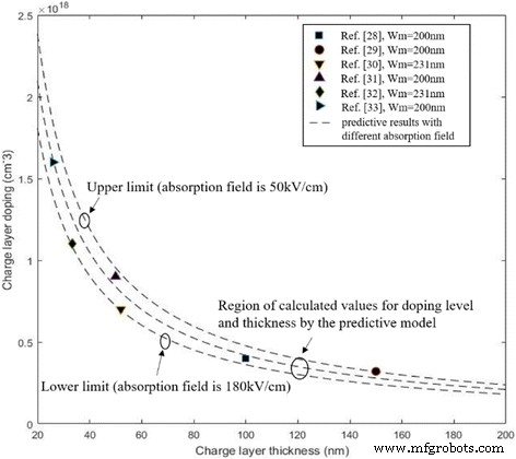
各种报告的理论结果和实验数据的比较 (w 米 =200 纳米)。封闭符号:参考文献中倍增厚度为 200 nm(黑色正方形、黑色圆圈、黑色三角形、黑色直指三角形)和 231 nm(黑色菱形、黑色向下指三角形)的电荷层的掺杂水平和厚度。通过公式 8(吸收场为 50-180 kV/cm)呈现电荷层的计算值(掺杂水平和厚度)。当吸收场为 50 kV/cm 时,可以获得电荷层中掺杂水平的上限。当吸收场为 180 kV/cm 时,可以获得电荷层中掺杂水平的下限。我们比较了各种报告的理论结果和实验数据。理论值区域与实验数据吻合良好。虚线为由公式计算的掺杂水平和厚度值
我们计算了不同厚度电荷层的最佳掺杂水平,倍增层为 300、500 和 700 nm,结果如图 3 所示。该结果说明电荷层中掺杂水平的容差为与它的厚度有关,掺杂水平的范围随着电荷层厚度的增加而减小。也就是说,如果我们应用较厚的电荷区,则电荷层中只会存在小范围的掺杂水平以满足最佳电场。因此,APD 的性能因较厚电荷层中掺杂浓度的几个百分比偏差而显着变化。在“结果与讨论”部分,模拟了 APD 的实际结构以研究和验证理论分析,其中包括电荷层厚度对电荷层中掺杂水平范围的影响以及不同电荷层厚度对电荷层的性能变化。 APD。
<图片>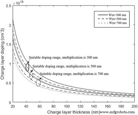
不同倍增层的最佳掺杂水平和电荷层厚度。实线:w 米 =300nm。虚线:w 米 =500nm。点线:w 米 =700 纳米。在吸收层场合适的情况下,通过公式给出电荷层的计算值(掺杂水平和厚度)。倍增层的厚度为 300、500 和 700 nm。当倍增层厚度一定时,我们可以用公式求出最佳的掺杂水平和电荷层厚度
考虑隧道效应的理论模型
上述分析模型是关于器件中电场分布的,基于ρ的前提 是耗尽层中的掺杂离子。如果吸收层内存在足够高的电场,则局部带弯曲可能足以允许电子隧穿 [34]。因此,可能发生电子隧穿。从图4的隧穿示意图可知,当吸收层发生击穿隧穿时,隧穿效应改变电荷密度ρ ,吸收中的正电荷增加,倍增层和电荷层中的负电荷增加。因此,ρ 不等于隧道效应出现时耗尽层中的掺杂离子电荷密度。前面讨论的公式在考虑隧道效应后会发生变化。
<图片>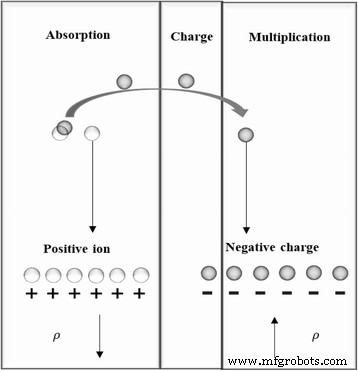
倍增层和吸收层中的隧道过程和电荷密度变化。给出了设备中隧穿过程的示意图。如果吸收层内存在足够高的电场,则局部带弯曲可能足以允许电子隧穿。当吸收层具有击穿隧穿时,吸收中的正电荷增加,倍增层和电荷层中的负电荷增加。因此,ρ 不等于耗尽层中掺杂离子电荷密度而出现隧道效应
生成率G bbt 带间隧道的定义见公式13[35, 36]。
$$ {G}_{bbt}={\left(\frac{2{m}^{\ast }}{E_g}\right)}^{1/2}\frac{q^2{E_p}^ {\gamma }}{{\left(2\pi \right)}^3{\hbar}^2}\exp \left(\frac{-\pi }{4{q\mathit{\hbar E}} _p}{\left(2{m}^{\ast}\times {E_g}^3\right)}^{\raisebox{1ex}{$1$}\!\left/ \!\raisebox{-1ex} {$2$}\right.}\right)=A\times {E_p}^{\gamma}\times \exp \left(-\frac{B}{E_p}\right) $$ (13)在公式 13 中,E g 是 InGaAs 的能带隙,m* (等于 0.04 m e ) 是有效减少的质量,E p 是吸收层的击穿电场,γ 是用户可定义的参数,通常限制为 1~2。 A 和 B 是表征参数。我们计算 G bbt 与不同的 γ , 结果如图 5 所示。可以发现 G bbt 对电荷层掺杂水平采用相同数量级,而 γ 限制在1~1.5。
<图片>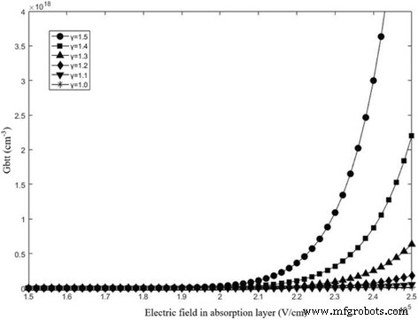
G btt 对于具有不同γ的吸收层中的不同场 . γ 的值 是 1.0(黑星)、1.1(黑色下指三角形)、1.2(黑色菱形)、1.3(黑色三角形)、1.4(黑色方块)、1.5(黑色圆圈)。显示 G 的计算结果 btt 由公式 13. 当吸收场超过 19 kV/cm 时,G bbt 逐渐增加。还可以发现 G bbt 对电荷层掺杂水平采用相同数量级,而 γ 限制在1~1.5
结果,电荷密度ρ 是一个变量,由隧道效应和吸收隧道中的掺杂离子决定。此时,公式1将变为公式14,乘法层中的电场将由公式15描述。w 隧道是隧穿过程的有效耗尽层[35]。因此,雪崩场的变化可以用公式16来描述,雪崩场随着隧穿效应的倍增而减小。
$$ \frac{d\xi}{dx}=\frac{\rho }{\varepsilon }=\frac{q\times \left(N+{G}_{btt}\right)}{\varepsilon }, {E}_p> 1.8\times {10}^5V/ cm $$ (14) $$ \xi \left(x,{V}_{\mathrm{bias}}\right)={\xi}_{ \max \left({V}_{\mathrm{bias}}\right)}+\frac{q\times \left({N}_1\times \left|x\right|+{G}_{bbt }\times {w}_{\mathrm{tunnel}}\right)}{\varepsilon_{s1}}\left(0\ge x\ge {X}_m\right) $$ (15) $$ \delta \xi \left(x,{V}_{\mathrm{bias}}\right)=\delta E=\frac{q\times {G}_{btt}\times {w}_{\mathrm{tunnel }}}{\varepsilon_{\mathrm{s}3}} $$ (16)电子和空穴电离系数由 [18] 中的公式 17 和 18 描述。 E 是乘法中的雪崩场。
$$ \alpha ={a}_n{e}^{\raisebox{1ex}{$-{b}_n$}\!\left/ \!\raisebox{-1ex}{$E$}\right.} $$ (17) $$ \beta ={a}_p{e}^{\raisebox{1ex}{$-{b}_p$}\!\left/ \!\raisebox{-1ex}{$E$ }\对。} $$ (18)载流子雪崩的影响由碰撞电离模型解释。考虑到倍增层的载流子密度与电荷层相比极低,可以合理地假设整个倍增层的电场是均匀的。因此,乘法因子 (M n ) 可以表示为以下等式。 19. 这里,w 米 是倍增层厚度和 k 是由 α/β 定义的碰撞电离系数比 .由于 k 随电场变化非常缓慢,k 对于 w 的轻微变化,近似恒定 米 [37].
$$ {M}_n=\frac{k-1}{k\times {e}^{-\alpha \left(1-\raisebox{1ex}{$1$}\!\left/ \!\raisebox{ -1ex}{$k$}\right.\right){w}_m}-1} $$ (19)假设常数 w 米 和偏置电压,M的微分 n 电子电离系数见式20和21。
$$ \delta {M}_n\left|{}_{w=const\&V=const}\right.={M_n}^2{e}^{-\alpha \left(1-\raisebox{1ex} {$1$}\!\left/ \!\raisebox{-1ex}{$k$}\right.\right){w}_m}\times {w}_m\delta \alpha $$ (20) $$ \delta \alpha =\frac{\delta \alpha}{\delta E}={\alpha}_n{b}_n{e}^{\frac{-{b}_n}{E}}\frac{1 {E^2} $$ (21)在公式20和21中,δα/δE 是积极的。假设总耗尽吸收层的 20% 是 w 隧道和吸收层是 400 纳米厚。通过求解公式 16,δE 之间的关系 以及不同γ的吸收场 如图 6 所示。可以发现 δE 在乘法中为雪崩场采用相同的数量级。因此,隧穿效应对雪崩场和M有影响。 n 会随着隧道效应而降低。在分析中,我们假设负电荷在乘法中是非乘法的,考虑到这一点,模型会更加严谨。为了验证和分析隧穿效应对APD实际结构的影响,我们在“结果与讨论”部分详细模拟了隧穿效应与倍增雪崩场之间的关系。
<图片>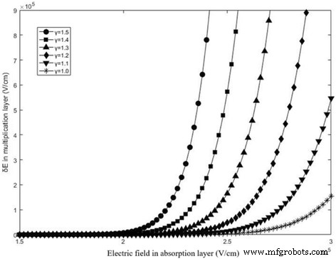
δE 对于具有不同γ的吸收层中的不同场 . γ 的值 是 1.0(黑星)、1.1(黑色下指三角形)、1.2(黑色菱形)、1.3(黑色三角形)、1.4(黑色方块)、1.5(黑色圆圈)。给出δE的计算结果 由公式 16. 当吸收场超过 19 kV/cm 时,δE 逐渐增加。还可以发现δE 在乘法中为雪崩场采用相同的数量级。由此可见,隧穿效应对雪崩场的影响具有隧穿效应
结构与仿真模型
TCAD的半导体器件模拟被用于模拟和分析。该仿真引擎定义了仿真中的物理模型,其结果具有物理意义[20]。基本物理模型如下所示。漂移扩散模型,包括泊松和载流子连续性方程,用于模拟电场分布和扩散电流 IDIFF。带间隧道电流IB2B采用带间隧道模型,陷阱辅助隧道电流ITAT采用陷阱辅助隧道模型。生成-复合电流 IGR 由 Shockley-Read-Hall 复合模型描述,俄歇复合电流 IAUGER 由俄歇复合模型描述。这些机制[38]清楚地描述了暗电流。 Selberherr 碰撞电离模型描述了雪崩倍增。其他基本模型,包括Fermi-Dirac载流子统计、载流子浓度相关、低场迁移率、速度饱和和射线追踪方法,用于仿真模型,并建立了严格的仿真模型。
模拟中的器件结构与[13]中的实验结构相似。顶照SAGCM InGaAs/InAlAs APD截面示意图如图7所示,结构从上到下依次为InGaAs接触层、InAlAs包覆层、InAlGaAs渐变层、InGaAs吸收层、InAlGaAs渐变层、InAlAs 电荷层、InAlAs 倍增层、InAlAs 包覆层、InP 接触层和 InP 衬底。每层的厚度和掺杂也如图 7 所示。为了避免厚度对模拟结果的影响,我们选择了两种模拟结构。一种模拟结构命名为APD-1(倍增层和吸收层分别为800和1800 nm),另一种模拟结构命名为APD-2(倍增层和吸收层分别为200和600 nm)。 <图片>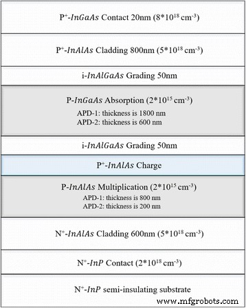
APD的仿真结构和参数。展示了顶部照明的 SAGCM InGaAs/InAlAs APD-1 和 APD-2 的横截面示意图。包括结构、材料、掺杂、厚度
为了测试仿真模型,将文献[13]中的实验数据与仿真结果进行了比较。在本次仿真中,我们使用了与参考文献相同的结构,并给出了器件的电流-电压特性。图 8 显示了我们的模拟结果和参考中的实验结果。它们具有相似的穿通电压 V pt 和击穿电压 V 兄弟此外,仿真结果与实验结果吻合良好。因此,我们模拟中的模型是准确的。上述参数列于表 1。
<图片>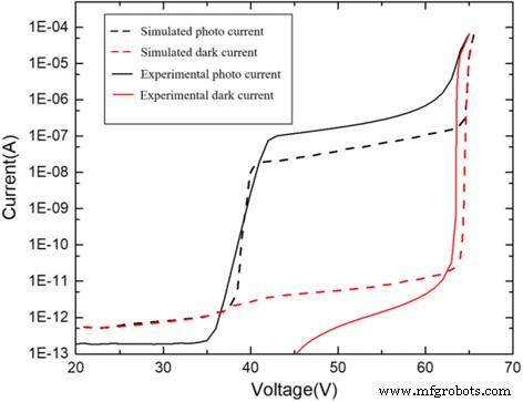
模拟结果与实验结果(光电流和暗电流)的对比。黑色虚线:模拟光电流。红色虚线:模拟暗电流。黑色实线:实验光电流。红色实线:实验暗电流。给出了模拟结果和实验结果的比较。仿真模型使用与参考文献中实验相同的参数
结果与讨论
本节对理论分析和结论进行了详细的仿真研究。首先,在“电荷层厚度的影响”部分研究了电荷层厚度对电荷层掺杂水平容限的影响。然后,在“隧道效应对电场分布的影响”部分分析并验证了隧道效应与倍增雪崩场之间的关系。
电荷层厚度的影响
根据 [14],InGaAs/InAlAs APD 中合适的场分布应符合这些规则。保证V pt <V br 和 V br − V pt 应具有处理温度波动和操作范围变化的安全裕度。在吸收层中,电场应大于 50-100 kV/cm,以确保光致载流子有足够的速度。同时,电场必须小于 180 kV/cm 以避免吸收层中的隧道效应。电场分布极大地影响器件性能。吸收层中电场的选择在小渡越时间、暗电流和高响应度之间权衡了实际需要。
In the simulation, we used the structure of APD-1 (multiplication is 800 nm thick) and adjusted the charge layer thickness from 50 to 210 nm to study the influence of charge layer thickness on doping level range and verify the theoretical conclusions in analytical model. In the simulation, we selected different doping level ranges in the charge layer so that the electric field distribution complies with the rules. The simulation results on the relationship between thickness and doping level range in the charge layer are presented in Fig. 9a. As the charge layer thickness increases, the suitable doping level range in charge layer decreases. A relatively large doping level range exists in the thin charge layer, and under this doping level range, the device will have a suitable electric field distribution. Apparently, the doping level range is determined by charge layer thickness. The simulation result of APD-2 (with a thickness of multiplication of 200 nm) is presented in Fig. 9b, which has a similar result. Moreover, it can be found that the calculated results of Fig. 2 and simulation results of Fig. 9b match well as shown in Fig. 9c. The small difference between the calculated results and simulation results is caused by the different values of avalanche field in the simulation and calculation. The avalanche field in simulation engine is used 6.4 × 10 5 V/cm, while in the calculation, we use the value of 6.7 × 10 5 V/cm from [27].

一 Relationship between suitable doping level and thickness of charge layer (APD-1). The thickness of charge layer is 50 nm (black square), 90 nm (black circle), 130 nm (black triangle), 170 nm (black down-pointing triangle), 210 nm (black diamond). 一 presents the suitable doping level region for different thickness of charge layer. As the charge layer thickness increases, the suitable doping level range in the charge layer decreases. A relatively large doping level range exists in the thin charge layer, and under this doping level range, the device will have a suitable electric field distribution. Apparently, the doping level range is determined by charge layer thickness. b Relationship between suitable doping level and thickness of charge layer (APD-2). The thickness of charge layer is 50 nm (black square), 70 nm (black circle), 90 nm (black triangle), 110 nm (black down-pointing triangle), 130 nm (black diamond), and 150 nm (black pentagon). The figure description of b is similar to a . c Comparison of calculated results in Fig. 2 and simulated results in Fig. 9b. Dashed line:calculated results. Closed symbols:simulated results (black square). c presents the comparison of calculated results in Fig. 2 and simulated results in Fig. 9b. The calculated results and simulated results correspond well
The charge layer thicknesses of 210 and 50 nm (APD-1) were selected to show the simulation details and the influence of doping level on the electric field distribution. Figure 10a, c shows the current simulation results of different doping levels in thicknesses of 210 and 50 nm, respectively. Figure 10b, d shows the electric field distribution simulation results using the same structure. The simulation results show that thicknesses of 210 and 50 nm have doping level ranges of 1.0 × 10 17 –1.3 × 10 17 cm −3 and 3.9 × 10 17 –5.7 × 10 17 cm −3 , respectively.

一 Photocurrent and dark current with different doping level (thickness of charge layer is 210 nm). Solid line:doping level in the charge layer is 1.3 × 10 17 cm −3 . Dashed line:doping level in charge layer is 1.15 × 10 17 cm −3 . Dashed dot line:doping level in charge layer is 1.0 × 10 17 cm −3 . 一 Presents the simulation results of currents with different doping level. The device with a charge layer thickness of 210 nm only has a relatively narrow and suitable doping level. A minimal change in the doping level has greatly influence the punch-through voltage, breakdown voltage, and current-voltage characteristic. b Avalanche field with different doping level (thickness of charge layer is 210 nm). Solid line:doping level in charge layer is 1.3 × 10 17 cm −3 . Dashed line:doping level in charge layer is 1.15 × 10 17 cm −3 . Dashed dot line:doping level in charge layer is 1.0 × 10 17 cm −3 . b Presents the simulation results of fields with different doping level. The device with a charge layer thickness of 210 nm only has a relatively narrow and suitable doping level. A minimal change in the doping level has greatly influenced the electric field distribution. c Photocurrent and dark current with different doping level (thickness of charge layer is 50 nm). Solid line:doping level in charge layer is 5.7 × 10 17 cm −3 . Dashed line:doping level in charge layer is 4.8 × 10 17 cm −3 . Dashed dot line:doping level in charge layer is 3.9 × 10 17 cm −3 . c Presents the simulation results of currents with different doping level. The device with a charge layer thickness of 50 nm has a relatively wide and suitable doping level. A minimal change in the doping level has a small influence on the current-voltage characteristic. d Avalanche field with different doping level (thickness of charge layer is 50 nm). Solid line:doping level in charge layer is 5.7 × 10 17 cm −3 . Dashed line:doping level in charge layer is 4.8 × 10 17 cm −3 . Dashed dot line:doping level in charge layer is 3.9 × 10 17 cm −3 . d Presents the simulation results of fields with different doping level. The device with a charge layer thickness of 50 nm only has a relatively wide and suitable doping level. A minimal change in the doping level has a small influence on the electric field distribution
Clearly, the device with a charge layer thickness of 210 nm only has a relatively narrow and suitable doping level. A minimal change in the doping level has greatly influence the current-voltage characteristic and electric field distribution. As a result, the performance of APD varies significantly via several percent deviations of doping concentrations in the thicker charge layer. This conclusion is the same as the theoretical analysis. Concurrently, when designing APD structures, choosing a thin charge layer will give a high level of doping tolerance, as well as confer APD with good controllability.
Finally, the relationship between charge layer and multiplication thickness was simulated. Figure 11a presents the avalanche field with multiplication region thicknesses of 100, 200, and 300 nm in the APD-2 structure (with a charge layer thickness of 70 nm). Figure 11b presents the charge layer doping range with different multiplication thicknesses at the suitable electric field distribution condition. The charge layer thicknesses are 50, 70, and 90 nm. Clearly, a high avalanche field exists in the thin multiplication layer. As the multiplication region thickness decreases, the electric field difference between multiplication and absorption layers increases. As a result, a thin multiplication layer needs a high product of the charge layer doping level and thickness to reduce the high avalanche field.

一 Avalanche breakdown electric field with different multiplication thicknesses. Solid line:w 米 = 100 nm. Dashed line:w 米 = 200 nm. Dashed dot line:w 米 = 300 nm. 一 Presents the simulation results of electric field distribution with different w 米 . As the w 米 decreases, the avalanche field in the multiplication increase. b Relationship between multiplication thickness and charge layer. The thickness of multiplication is 300 nm (black square), 200 nm (black circle), 100 nm (black triangle). b Presents the relationship between multiplication thickness and charge layer. A thin multiplication layer needs a high product of the charge layer doping level and thickness to reduce the high avalanche field
Tunneling Effect on the Electric Field Distribution
The simulation in this part will study the tunneling effect on the electric field in the device. From the theoretical analysis, the tunneling effect has an influence on the avalanche field in multiplication. Thus, the simulation will design to study the influence of electric field in the absorption layer that exceeds the tunneling threshold value. First, group A, with the structure of APD-1, charge layer thickness of 90 nm, and different charge layer doping levels of 1.4 × 10 17 –2.4 × 10 17 cm −3 , was simulated for electric field distribution when the device avalanche breaks down. The result is shown in Fig. 12a. When the charge layer doping level exceeds 2.0 × 10 17 cm −3 , the field in the absorption layer becomes lower than the tunneling threshold field and the avalanche field in the multiplication layer reaches the same value. However, when the doping level is less than 2.0 × 10 17 cm −3 , the field in the absorption layer exceeds the tunneling threshold field and the avalanche field in the multiplication layer decreases with the decrease of the doping level in charge layer. Similar results were observed in the APD-2 structure (with a charge layer thickness of 90 nm and doping level of 2.2 × 10 17 –3.6*10 17 cm −3 ) (Fig. 12b). That is, if the electric field in the absorption layer exceeds the tunneling threshold value at or over the breakdown voltage, then the breakdown electric field in the multiplication will decrease.

一 Avalanche breakdown electric field with different doping levels (APD-1). Thickness of charge layer is 90 nm. Red dashed lines:the field of absorption is larger than the tunneling threshold field. Black solid lines:the field of absorption is less than the tunneling threshold field. 一 Presents the simulation results of electric field distribution with different doping level while avalanche breakdown. When doping level of charge layer exceeds 2.0 × 10 17 cm −3 , the field in the absorption layer becomes lower than the tunneling threshold field, and the avalanche field in the multiplication layer reaches the same value with different doping level. However, when the doping level is less than 2.0 × 10 17 cm −3 , the field in the absorption layer exceeds the tunneling threshold field, and the avalanche field in the multiplication layer decreases with the decrease of the doping level. Thus, if the electric field in the absorption layer exceeds the tunneling threshold value at or over the breakdown voltage, then the breakdown electric field in the multiplication will decrease. Thus, the electric field in the absorption should be less than the tunneling threshold value to maintain the high field in the multiplication layer when the device avalanche breaks down. b Avalanche breakdown electric field with different doping levels (APD-2). Thickness of charge layer is 90 nm. Red dashed lines:the field of absorption is larger than the tunneling threshold field. Black solid lines:the field of absorption is less than the tunneling threshold field. The figure description of b is similar to a . c Relationship between field and bias voltage in multiplication and absorption (APD-1). Thickness of charge layer is 90 nm. Electric field of multiplication (black square). Electric field of absorption (red triangle). c Presents the relationship between the electric field and bias voltage in multiplication and absorption layers. When the electric field in the absorption layer reaches the tunneling threshold value, the avalanche breakdown electric field in the multiplication gradually decreases. Moreover, the absorption field slope increases when the electric field in the absorption layer exceeds the tunneling threshold. d Relationship between field and bias voltage in multiplication and absorption (APD-2). Thickness of charge layer is 90 nm. Electric field of multiplication (black square). Electric field of absorption (red triangle). The figure legend of d is similar to a
Groups B (APD-1 thickness of 90 nm, doping level of 2.4 × 10 17 cm −3 in charge layer and APD-2 thickness of 90 nm, doping level of 3.6 × 10 17 cm −3 ) were designed to demonstrate the relationship between the threshold electric field in the absorption layer and avalanche field in the multiplication layer. The multiplication and absorption electric fields vary with the bias voltage on the device. As shown in Fig. 12c, d, when the electric field in the absorption layer reaches the tunneling threshold value, the avalanche breakdown electric field in the multiplication gradually decreases. Moreover, when the absorption field exceeds the tunneling threshold, the avalanche breakdown electric field in the multiplication layer plummets. Furthermore, the absorption field slope increases when the electric field in the absorption layer exceeds the tunneling threshold.
The phenomenon in Fig. 12 can be explained by the theoretical analysis that tunneling has an influence on the charge density in the “Methods” section. When the electric field reaches the tunneling threshold value in the absorption layer, the charge density ρ becomes unequal to the dopant ion. The multiplication field will decrease as the negative ion increases, and the absorption field will increase as the positive ion increases. Concurrently, the absorption field slope will increase due to the tunneling effect. As a result, the electric field in the absorption should be less than the tunneling threshold value to maintain the high field in the multiplication layer and the low dark current when the device avalanche breaks down.
Conclusions
In summary, we have presented a theoretical study and numerical simulation analysis involving the InGaAs/InAlAs APD. The mathematical relationship between the device parameters and electric field distribution in the device was built. And the tunneling effect was taken into consideration in the theoretical analysis. Through analysis and simulation, the influence of structure parameters on the device and the detailed relationship of each layer were fully understood in the device. Three important conclusions can be obtained from this paper. First, the doping level and thickness of the charge layer for different multiplication thicknesses can be calculated by the theoretical model in the “Methods” section. Calculated charge layer values (doping and thickness) are in agreement with the experiment results. Second, as the charge layer thickness increases, the suitable doping level range in charge layer decreases. Compared to the thinner charge layer, the performance of APD varies significantly via several percent deviations of doping concentrations in the thicker charge layer. When designing APD structures, choosing a thin charge layer will give a high level of doping tolerance, as well as confer APD with good controllability. Finally, the G btt of tunneling effect was calculated, and the influence of tunneling effect on the avalanche field was analyzed. We confirm that the avalanche field and multiplication factor (M n ) in the multiplication will decrease by the tunneling effect.
缩写
- 2D:
-
Two-dimensional
- APD:
-
Avalanche photodiode
- DCR:
-
Dark count rate
- SACM APDs:
-
Separate absorption, charge, and multiplication avalanche photodiodes
- SAGCMAPDs:
-
Separate absorption, grading, charge, and multiplication avalanche photodiodes
- SPAD:
-
Single-photon avalanche photodiode
- SPDE:
-
Single-photon detection efficiency
- SRH:
-
Shockley–Read–Hall
纳米材料
- 用于 Micro-LED 和 VCSEL 的高级原子层沉积技术
- 电子倍增器发射层的设计
- 通过等离子体增强原子层沉积制备的 Co3O4 涂层 TiO2 粉末的光催化性能
- 双轴拉伸应变锗纳米线的理论研究
- 通过界面层设计调整 ZnO 薄膜的表面形貌和特性
- 通过超循环原子层沉积调节 ZnO 薄膜的费米能级
- 背面有黑硅层的晶体硅太阳能电池的研究
- 1.3–1.55-μm 窗口中变质 InAs/InGaAs 量子点的带间光电导率
- Si、Ge 和 Si/Ge 超晶格对低能辐射的辐射响应的理论模拟
- InGaAs/InP 核壳纳米线的自种 MOCVD 生长和显着增强的光致发光
- 固体源两步化学气相沉积法制备 InGaAs 纳米线的形成机制
- 蚀刻变化对 Ge/Si 沟道形成和器件性能的影响