

通过金属纳米孔阵列的表面等离子体效应实现量子点红外光电探测器的高光子吸收率
摘要
随着对小型光电探测器器件的需求不断增加,基于量子点的红外光电探测器在过去几十年中受到越来越多的关注。在这项工作中,周期性金属纳米孔阵列结构被引入到量子点红外光电探测器中,通过表面等离子体增强效应来增强光子吸收性能,以克服传统光电探测器中存在的光吸收效率低的瓶颈。结果表明,优化后的金属纳米孔阵列结构可以使特定光电探测器的光子吸收率大幅提高至 86.47%,是没有金属阵列结构的传统光电探测器的 1.89 倍。吸收率的大幅提高可归因于金属纳米孔阵列结构引起的局部耦合表面等离子体效应。相信该研究可为基于纳米量子点的高性能红外光电探测器提供一定的理论指导。
背景
半导体红外光电探测器可用于探测红外光,在科学研究、数字成像、光通信、军事等领域有着广阔的应用前景。迄今为止,量子点红外光电探测器 (QDIP) 由于其出色的光响应特性和器件小型化趋势,近年来受到越来越多的关注 [1,2,3]。尽管科学家们数十年的持续努力在开发获得高性能 QDIP 的技术方面取得了很大进展,但仍需要进一步改进以应对器件小型化的挑战 [4] 和实际需求。有人指出,在基于量子点的有源区上耦合金属光栅可以被视为提高 QDIP 性能的有效方法 [5, 6],它可以通过等离子体增强的局部光耦合产生高光吸收系数。
据报道,有两种主要的金属光栅结构用于提高 QDIP 的性能。一种是金属孔阵列结构,另一种是无孔金属阵列结构。更具体地说,在金属孔阵列结构的应用方面,2007年Chang课题组在QDIP中将金属孔周期阵列与量子点层相结合,实现了光电探测器的超常光透射[7]。 2009 年,Lee 等人。提出了一种通过将金属光子晶体与 3.6-μm 周期的孔阵列(100-nm 厚度)集成来实现高探测 QDIP 的方法[8]。研究结果表明,该方法可以实现光电探测器在11.3 μm波长处的峰值响应,探测率比没有金属光子晶体的方法提高30倍。然后,他们讨论了 QDIP 依赖于入射光的性能及其在焦平面阵列中的应用 [9, 10]。通过使用孔金属阵列耦合光栅,在报告中也可以发现类似的性能增强 [11,12,13,14]。还提出了无孔金属阵列结构。 2011年,Huang等人利用自组织等离子体银纳米粒子层增强QDIP的宽光谱响应,获得了2.4~3.3倍的增强[15]。 2014 年,Chen 的团队报告说,可以通过 Au 纳米粒子的近场效应来增强光电探测器的性能 [16]。 2015年,Ding课题组和Wang课题组分别提出了分布式布拉格反射器的波导耦合结构和单谐振腔[17, 18]。除上述结构外,还讨论和分析了其他金属结构,例如天线带阵列和纳米盘阵列[19,20,21]。
然而,这些无孔阵列方法也可以在 QDIPs 的光响应中表现出增强的效果,但与典型的孔阵列结构相比,其具有成本效益和简单方法的制造工艺仍然是一个挑战。对于典型的孔阵列结构,孔阵列的尺寸在微观尺度上是常见的。光响应增强是通过微尺度金属孔中的空气与下面的半导体之间的界面处的等离子体效应来实现的。无论是否能够实现具有相应增强效果的高性能 QDIP,金属孔阵列尺寸都可以进一步减小到与纳米级 QDIP 中量子点尺寸匹配的预期纳米级。同时,还需要进一步的理论工作来阐明这些现象背后的机制。在本研究中,为了清楚地说明这一现象,设计了具有纳米级金属孔阵列结构的 QDIPs,与传统的微米级 QDIPs 相比更重要的是,通过分析光传输条件和电场分布来解释增强效应.结果表明,由于光子-量子点相互作用和有效的光耦合,具有纳米级金属阵列结构的 QDIPs 的光子吸收率可高达 86.47%,这可能为纳米级红外的设计和优化打开大门。光电探测器。
纳米孔阵列QDIP设计模型
一般来说,QDIP由量子点区和电极组成,量子点区由周期量子点层和势垒层组成。在理想条件下(忽略电极和基板的影响),整个 QDIP 的光传输可以假设等于量子点区域的光传输。因此,在 QDIP 的设计中不需要出现电极和基板。具体来说,图1a给出了典型的QDIP的设计,它由5个周期的量子点复合层组成,这些复合层由AlGaAs势垒层和包含周期量子点的GaAs层构成(图1a)。 1b)。在目前的配置中,量子点纳米粒子被假设为立方体形状,符合由许多原子和分子形成的量子点的定义,长度为40 nm,宽度为40 nm,7~9 nm 的高度。在报道的文献[22]中也可以找到类似的量子点模型。 QDIP的面积设置为1000 nm×1000 nm,AlGaAs势垒层的厚度为60 nm。选择Au的金属纳米孔阵列放置在常规QDIP的常规量子点纳米结构层上,称为改进的QDIP,如图2所示。孔的半径可在50~70 nm范围内调整.需要注意的是,不能简单地将构成量子点的材料视为具有一定折射率的块状材料。图 3 显示了使用 Edward D. Palik [23] 的方法形成量子点的 GaAs 材料的电色散特性。图中蓝色曲线和红色曲线代表GaAs的介电常数ε ′ 和 ε ″ , 分别。图4a、b分别为GaAs、Al0.3Ga0.7As材料和金材料的电色散特性。
<图片>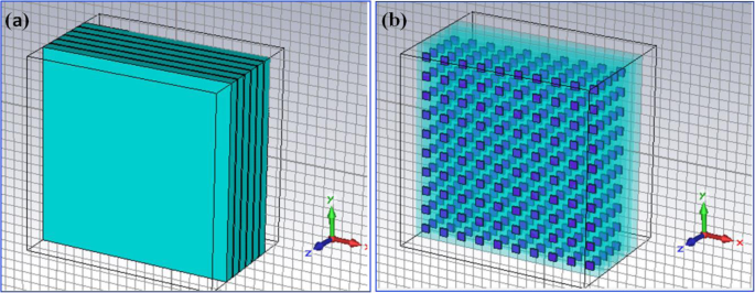
一 典型量子点红外光电探测器的结构模型图。 b 具有 5 周期量子点复合层的有源区中的量子点分布。这些复合层由AlGaAs势垒层和GaAs层构成
<图片>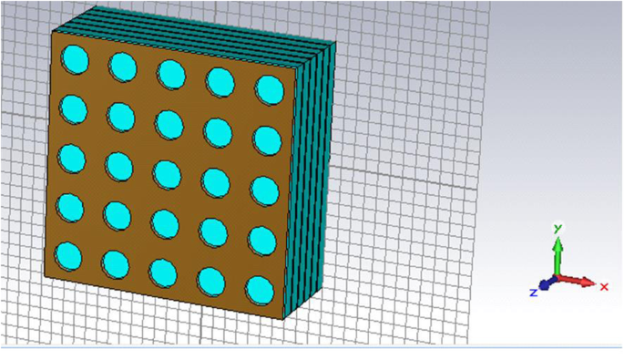
用于改进QDIP的具有周期性金属纳米孔阵列结构的量子点有源区

GaAs材料的色散关系
<图片>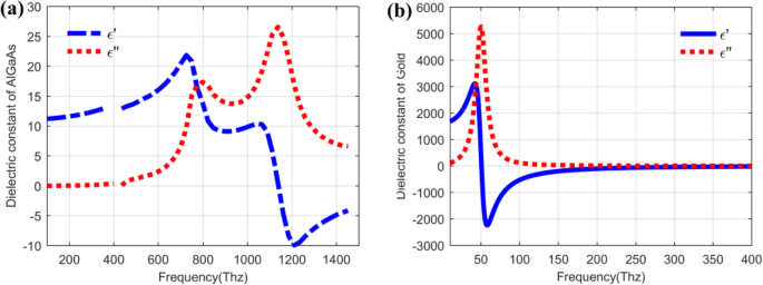
一 AlGaAs 材料的色散关系。 b Au材料的色散关系
基于YEE Cell的计算方法
基于上述设计的物理模型,采用有限元积分法计算光传输条件。首先,基于YEE单元,将满足上述模型的麦克斯韦积分方程写成:
$$ {\oint}_LE\cdot dl=-\frac{\partial }{\partial t}{\int}_SB\cdot dS $$ (1) $$ {\oint}_LH\cdot dl=J+\frac {\partial }{\partial t}{\int}_SD\cdot dS $$ (2) $$ {\oint}_SD\cdot dS=q $$ (3) $$ {\oint}_SB\cdot dS=0 美元 (4)在我们的计算中,方程。 1-4 被离散化。电场节点和磁场节点的分布均选择为“Yee cell”格式。使用方程。以图1为例,光电探测器的电磁模型可以看作是“Yee cell”的积累。如图 5 所示,任意单元格的四个边对应于等式。 1,表示电场矢量e 我 ,e j ,e k , 和 e l .位于法线方向的矢量是磁场矢量b n ,因此前面的方程。 1 可以改写为以下等式。 5.
$$ {e}_i+{e}_j-{e}_k-{e}_l=-\frac{db_n}{dt} $$ (5)
“YEE细胞”示意图
采用类似的方法,整个光电探测器的电磁模型方程可写为:
$$ \left[\begin{array}{l}..\dots \dots \dots \dots \dots \dots \dots \\ {}1\kern0.5em 1\kern0.5em -1\kern0.5em - 1\\ {}.\dots\dots\dots\dots\dots\dots\dots\\{}.\dots\dots\dots\dots\dots\dots\dots\end{array}\right]\left[ \begin{array}{l}{e}_i\\ {}{e}_j\\ {}{e}_k\\ {}{e}_l\end{array}\right]=-\frac{d {dt}\left[\begin{array}{l}.\\ {}{b}_n\\ {}.\\ {}.\end{array}\right] $$ (6)等式2也可以改写为:
$$ Ce=-\overset{.}{b} $$ (7)根据类似的方法,其他Eqs. 2 ~ 4 可以离散化为:
$$ \overset{\sim }{C}h=\overset{.}{d}+j $$ (8) $$ sb=0 $$ (9) $$ \overset{\sim }{S}d =q $$ (10)结合离散化的方程。 7-10 有边界条件,电场和磁场可以用迭代法求解。在这项研究中,金属孔阵列结构放置在传统 QDIP 的顶部,因此,该结构可以通过布拉格散射促进光耦合。进一步计算相应的光通信,当给出透射、反射和吸收的条件时,可以在下一节中讨论。此外,基于吸收和量子效率之间的关系,可以给出 QDIP 的响应度。具体地说,众所周知,QDIP 的响应率作为一个非常重要的性能参数,可以通过光电流与入射光功率的比值来计算 [24]。所以可以写成:
$$ R=\frac{I_{photo}}{P_o}=g\frac{\eta e}{hv} $$ (11)其中我 照片 是 QDIP 的光电流,P 是入射光的功率,g 是光电导增益,e 是电子的电荷,h 是普朗克常数,v 是入射光的频率,η 是量子效率。
量子效率可以定义为电子空穴数与入射光数之比,它强烈依赖于光电探测器的吸收。在实践中,由于入射光直接照射吸收区,由于顶部接触层或金属层的反射,它不能被完全吸收[25, 26]。因此QDIP的量子效率可以写为:
$$ \eta =\left(1-r\right)\left[\exp \left(-{\alpha}_0d\right)\right]\left[1-\exp \left(-{\alpha}_0W \right)\right] $$ (12)其中 α 0W 是 QDIP 的吸收系数,α 0d 是入射接触层的吸收系数,r 分别为入射层的反射。
在 QDIP 中,光电导增益可以定义为电子从扩展态回到量子点的复合时间之比 τ 生活 到电子穿过器件的传输时间 τ 总计 , 可以表示为:
$$ g=\frac{\tau_{life}}{\tau_{total}} $$ (13)在跨越量子点复合层一个周期的渡越时间远小于从扩展态回到量子点的复合时间的条件下[22, 27],增益可写为:
$$ g=\frac{\left(K+1\right) L\mu E{\left[1+{\left(\mu E/{v}_s\right)}^2\right]}^{ \hbox{-} 1/2}}{\mathrm{K}\pi {a}_{QD}^2{h}_{QD}^2{\sum}_{QD}{V}_{\数学{t}}} $$ (14)其中 K 是数字是量子点复合层,L 是量子点层之间的距离,μ 电子的迁移率,E 是 QDIP 上的电场密度,v s 是电子的饱和速度,h QD 是量子点的高度,∑QD 是每个量子点层中的量子点密度,a QD 是量子点的横向尺寸,V t分别为电子的俘获率。
提交方程(12) 和方程。 (14) 进入方程。 (11),我们可以得到QDIP的响应度,可以表示为:
$$ R==\frac{\lambda \left(K+1\right) L\mu E{\left[1+{\left(\mu E/{v}_s\right)}^2\right] }^{\hbox{-} 1/2}\left(1-r\right)\exp \left(-{\alpha}_0d\right)\left[1-\exp \left(-{\alpha} _0W\right)\right]}{1.24\mathrm{K}\pi {a}_{QD}^2{h}_{QD}^2{\sum}_{QD}{V}_{\mathrm {t}}} $$ (15)结果与讨论
基于上述 QDIP 的设计,如果入射红外光照射在 z 中这些 QDIP 的顶部 轴方向,光电探测器将反射和透射入射光。通过研究入射光的这些光传输条件,可以确定光电探测器的吸收率,这对评价光电探测器的性能具有非常重要的作用。图 6 显示了没有金属阵列(传统 QDIP)和有金属阵列(改进的 QDIP)的光电探测器的反射条件。对比图 6 中的两条曲线,可以发现,除了 250~260 THz 和 279~293 THz 频率范围内的个别值外,常规 QDIP 的反射系数值略小于改进 QDIP 的反射系数值.具体以219 THz频率值为例,传统QDIP的反射系数值为-3.91 dB,而改进的QDIP则低至-1.31 dB。如上所述,改进的QDIP可以具有比传统QDIP略高的值,但是可以发现改进的QDIP的最小吸收比传统的QDIP小很多。具体而言,改进的 QDIP 在 255.10 THz 频率下的最小吸收为 - 16.17 dB,而传统 QDIP 的值在 254.86 THz 时等于 - 13.42 dB。改进的 QDIP 的低反射系数可归因于金属对红外光的吸收系数高于半导体。可以根据反射和透射的共同贡献计算出吸收。图 7a 描绘了传统 QDIP 的透射系数,在 200~340 THz 的总频率范围内,它们用蓝色标记的值明显大于改进的 QDIP。例如,在298 THz频率下,改进后的QDIP传输系数仅为-10.83 dB,比传统QDIP传输系数-4.15 dB小1.60倍。根据透射、反射和吸收之间的竞争关系,在忽略入射光其他损耗的情况下,透射系数的降低会导致吸收的增加。
<图片>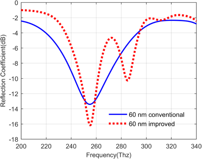
无金属阵列的常规QDIP(蓝色曲线)和带有金属纳米孔阵列的改进QDIP(红色曲线)的反射系数
<图片>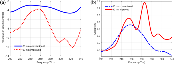
透射系数 (a ) 和吸收系数 (b ) 分别为常规 QDIP 和改进 QDIP
结合图 7a 中的传输情况和图 6 中的反射情况,可以计算 QDIP 的吸收率,如图 7b 所示。图中红色曲线(标记为60 nm改进)描述了具有金属结构的改进QDIP的吸收率,另一条蓝色曲线代表了没有金属孔结构的常规QDIP(标记为60 nm常规)。比较两条曲线,可以发现改进的QDIP的吸收率高于传统的QDIP。改进后的 QDIP 在 286 THz 频率下的最大吸收率为 0.782,是传统 QDIP 的 1.71 倍,后者在 257 THz 频率下仅为 0.458。改进后的 QDIP 吸收率增加的原因可以解释如下。金属纳米孔阵列结构被引入到常规 QDIP 的顶部,这种配置有利于表面等离子体共振效应,导致入射光的局部耦合效应。此外,局部耦合效应可以使更多的入射光进入下面的半导体量子点层,从而导致对入射光的高吸收,具有更好的光电特性,具有更大的光电流和更高的量子效率。
为了进一步明确如何在改进的 QDIPs 中实现等离子体增强效应,我们还研究了不同金属纳米孔结构对改进 QDIPs 吸收率的影响。如图 8a 所示,具有不同金属纳米孔半径的改进 QDIP 的吸收率曲线分别对应于黑色(50 nm)、绿色(55 nm)、红色(60 nm)和蓝色(65 nm)曲线。改进后的 QDIP 的吸收率值揭示了不同纳米孔下的不同变化趋势。改进后的 QDIP 的吸收率峰值分别为 0.744(289 THz 处的黑色曲线)、0.721(291 THz 处的绿色曲线)、0.782(286 THz 处的红色曲线)和 0.707(288 处的蓝色曲线) 。显然,在这些光电探测器中,孔半径为 60 nm 的改进型 QDIP 具有最佳的吸收性能。同时众所周知,金属孔层的厚度也会对吸收率产生影响。如图 8b 所示,当改进的 QDIP 中金属层的厚度从 10 变为 40 nm 时,吸收率的峰值相应地从 0.667(263 THz 为 10-nm 厚度)变为 0.782(286 20 nm 的 THz)、0.662(30 nm 的 293 THz)和 0.590(40 nm 的 262 THz)。在这些峰值中,厚度为20 nm的金属纳米孔层的吸收率值最高。
<图片>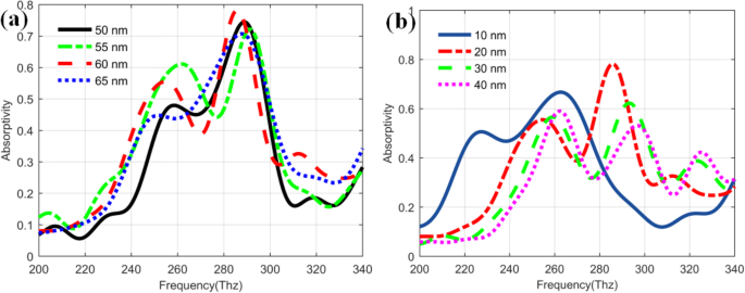
改进的 QDIP (a ) 具有不同半径和不同金属厚度的金属纳米孔 (b)
为明确上述现象,我们进一步研究了不同半径金属孔洞在286 THz处的改进QDIP顶面的电场分布情况。图 9 揭示了金属孔在 50-65 nm 范围内不同半径处的电场分布。比较图 9a 中的四张图片,很明显孔半径为 50 nm(图 9a)和 55 nm(图 9b)的 QDIP 可以具有相对较弱的电场增强,这是由于相应的电场分布在图 9 a和b位于包括孔洞及其相邻区域在内的整个区域,因此可以忽略它们的电场局部耦合效应,而在图9中可以观察到具有高电场的电场的局部耦合区域. 9 c 和 d。由于表面等离子体耦合效应,图9c和d中具有环形形状的孔周围的强电场分布可以位于金属孔和金属孔中的空气之间的界面上。与图 9c 和 d 中的电场分布相比,图 9c 中的电场耦合效应比图 9d 中的强,根据它们的标记颜色是红色、绿色和蓝色的混合。在这方面,红色代表最强的场,蓝色代表最弱的场。根据以上分析,半径为 60 nm 的金属纳米孔确实通过表面等离子体产生了增强电场效应。为了进一步使增强效果更加清晰,xz上的电场分布 -平面对应于我们研究中优化 QDIP 在 286 THz 频率下的最大吸收,如图 10a 所示,位于截面 y =0(对应xz的字段 -飞机)。图中,从z方向 轴,增强的电场分布在相邻金属孔之间的区域用红色标记,弱场位于金属孔用蓝色标记的区域。电场分布直接揭示了 QDIP 的增强吸收。正是增强耦合效应导致了吸收率的增加,进而导致了改进的 QDIP 的高量子效率。当然,根据光的电磁特性来分析磁场分布也可以得出同样的结论。由于对磁场分布的讨论与对电场分布的讨论相同,本研究无需讨论。
<图片>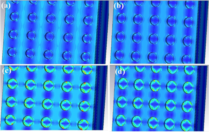
具有不同金属纳米孔半径的改进 QDIPs 的电场分布:a r =50 nm, b r =55 nm, c r =60 nm,和 d r =65 nm
<图片>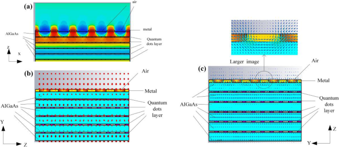
一 x - 优化 QDIP 的方向电场。 b 改进的 QDIP 的电场极化。 c 改进型QDIP的磁场极化
另外,如上所述,增强效应来自表面等离子激元,进一步确定了被激发的表面等离子激元波的模式。图 10a 和 b 显示了电场和磁场结果。在图中,图 10b 展示了电场在 yz 上的极化分布 -飞机。可见电场垂直于yz -平面,也就是说,电场不能有E z 分量。图 10c 显示了磁场的极化分布。可以发现磁场平行于yz -平面,也就是说,在入射光的传播方向上存在Hz分量,即z -方向。因此,在我们的研究中,激发的表面等离子体波是 TE 模式。此外,为了明确用于激发表面等离子体的位置,金属孔界面附近的磁场分布显示在图 10c 的顶部。可以看出,相邻金属孔之间的磁场强于金属孔中的磁场。另外,根据图10a中出现的电场,也可以证明增强场集中在相邻金属孔之间的位置。因此可以得出结论,表面等离子体效应可能来自金属和半导体之间的表面,该表面位于相邻金属孔之间的位置。当然,值得注意的是,吸收的增强不仅来自表面等离子体,也来自金属层的增强反射,导致入射光的二次吸收,因为入射光沿着 QDIP 照射在 QDIP 上。 z轴。
众所周知,与金属层相关的参数也会对 QDIP 的性能产生很大影响。为了确定最佳参数,在优化的金属层厚度(20 nm)和金属孔半径(60 nm)条件下,进一步分析和讨论了势垒层和量子点层的厚度。图11a描绘了在70-85 nm范围内不同厚度的势垒层的光电探测器吸收率的变化趋势。从图像上看,这些吸收率曲线具有相似的变化趋势。当势垒层的厚度在 70~85 nm 范围内变化时,相应的改进 QDIPs 的最大吸收率值为 0.7581 (70 nm, at 322.78 Thz), 0.7763 (75 nm, at 304.85.85 Thz) nm,分别在 292.75 THz)和 0.8346(85 nm,在 284.17)。与这些最大吸收率值相比,可以发现厚度为 80 nm 的势垒层对于改进的 QDIP 具有最佳的吸收率性能。将其他参数固定为上述优化值,进一步研究了量子点层厚度对改进QDIP吸收性能的影响,相应曲线如图11b所示。从图中可以发现,对于层厚为 7 nm 的改进 QDIP,红色曲线在 295.48 THz 频率下的最大吸收率为 0.8647,说明光电探测器可以具有最佳跃迁态。
<图片>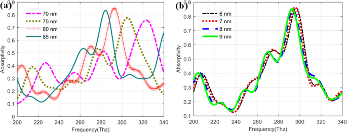
不同厚度a的改进QDIP的吸收率 量子点层和b 阻挡层
综上所述,不仅QDIP相关参数对器件性能有影响,量子点层和势垒层的厚度也能决定器件性能。在本研究中,根据理论计算结果,改进后的 QDIPs 的优化参数为金属层厚度为 20 nm,金属孔半径为 60 nm,量子点层厚度为 7 nm,势垒层为厚度为 80 nm。最佳光电探测器的吸收率可高达0.8647。此外,将传统 QDIP 与优化 QDIP 进行比较,如图 12 所示,除了 222.91~262.18 THz 频率范围内的值外,红色曲线中的吸收率值远高于蓝色曲线中的吸收率值。红色曲线的最大吸收率在 295.48 THz 频率处为 0.8647,是蓝色曲线的 1.89 倍(与图 7b 中标有“60 nm 常规”的上一条曲线相同,对应于没有金属孔阵列的 QDIP)在 257 THz 的频率。最大吸收峰的频移主要是由改进的光电探测器厚度的变化引起的。此外,基于优化后的QDIPs参数,计算出量子点层和势垒层的厚度,计算出光电探测器的量子效率值和响应度。

Absorptivity of the conventional QDIP in blue curve and improved QDIP in red curve with the barrier layer thickness of 80 nm
Quantum Efficiency and Responsivity of the QDIP
Based on the calculated results of the absorptivity in Fig. 12 as well as combining with the expression of the quantum efficiency and the responsivity of the QDIP above, the quantum efficiency of the QDIP and the responsivity can be calculated out, and the corresponding results are plotted in Fig. 13 a and b. Figure 13a depicts the quantum efficiency of the QDIP. In this figure, the blue dotted curve represents the quantum efficiency of the QDIP without metal array, the other red full curve is that of the optimized QDIP with metal array. Making a comparison between the two curves, it can be observed that the maximum quantum efficiency of the optimized QDIP is 0.2961 at the frequency of 295.87 Thz, and it is 1.205 times than that of the conventional QDIP, which is equal to 0.2458 at the frequency of 256.48 Thz. The increasing trend is similar to the absorptivity provided in Fig. 12 which results from the introduction of the metal hole array and the optimization of the quantum dot infrared photodetector. Based on the increasing trends for the absorptivity, we can find that the responsivity of the QDIP also reveals similar increasing trends. To be specific, Fig. 13b gives the responsivity of the optimized QDIP and the conventional QDIP, respectively. In the figure, the red curve is on behalf of the responsivity of the conventional QDIP, and the blue curve stands for that of the optimized QDIP with the metal holes layer. Similar to the analysis in Fig. 13a, the responsivity is 0.0326 mA/W at the frequency of 295.87 Thz, which is 0.0174 larger than that of the conventional QDIP at the frequency of 256.48 Thz (which is 0.0152). The increase in the responsivity can be proven in the other frequency band in the range of 229.57~254.41 Thz, which obviously demonstrates the enhancement in the performance of the photodetector due to the introduction of the metal hole array and the optimization of the quantum dot regions. Moreover, the reasons for the enhancement were detailedly discussed in detail analyzing the electric field distribution of quantum dot regions above.

一 Quantum efficiency of QDIP. b Responsivity of QDIP
Influence of the Electrodes and the Substrate
What was studied above is all under the condition of ignoring the influence of the electrodes and the substrate; in fact, the electrodes and the substrate can have certain influences on the performance, but they do not influence the description of the enhancement effects of the performance of the optimized QDIP with the metal layer. This is because the electrodes and the substrate can have almost the same influence on the absorption of the QDIP with the metal layer and without the metal layer. To illustrate the issue adequately, we recalculated the absorption of the QDIP considering the influence resulting from the substrate and the electrodes as well as the quantum efficiency, the responsivity, and so on. To be concrete, it is well known that the electrodes are generally designed at the two ends of the absorption region of the quantum dots, and thus, as shown in Fig. 14a, one is at the top of the conventional QDIP and the other is at the bottom end of the absorption region of the QDIP. That is to say, it lies at the top of the substrate, which can provide the quantum dot absorption region with the bias voltage and transmit current together with the electrodes said above. Here, it is worth mentioning that there is the metal hole array instead of the metal ring in the optimized QDIP in our study used as the electrodes. The other electrode is similar to that of conventional QDIP. Based on the above design, a concrete distribution of the electrodes is clearly calculated in Fig. 14a. Similar to Fig. 14a, in Fig. 14 b, the material of the electrodes is chosen as gold, and the substrate is chosen as AlGaAs; their thicknesses are 20 nm and 300 nm, respectively.

一 Conventional QDIP with electrodes and substrate. b Optimized QDIP with the electrodes and substrate
Based on the introduction of electrodes and substrate in the structure of the QDIP above, we calculated the absorption of the QDIPs, and the corresponding results are compared with the QDIP without the electrodes and the substrate. Figure 15 demonstrates the influence of the electrodes and substrate on the absorptivity of the QDIP. In the figure, the blue curve and the pink curve are the absorptivity of the conventional QDIP without the electrodes and the substrate and that of the optimized QDIP without the electrodes and the substrate, respectively. The red dashed curve represents the absorptivity of the optimized QDIP with the electrodes and the substrate. Its maximum absorption is 0.7620 at the frequency of 304.35 Thz which is just 0.1027 smaller than that of the optimized QDIP without electrodes and substrate. The decrease of the absorptivity is degraded from the loss of the electrodes and the substrate, the same as the green curve with the absorptivity of the conventional QDIP with the electrodes and substrate. Compared with the absorptivity of the conventional QDIP and optimized QDIP with electrodes and substrate, the enhancement is very clear in the absorptivity of the optimized QDIP with electrodes and substrate, which is the same as the optimized QDIP in Fig. 12. In other words, though the electrodes and the substrate can result in the decrease of the absorptivity, the total absorptivity of the optimized QDIP can be enhanced compared with that of bare QDIP, and thus, the decrease can be negligible as they can have a very small influence on the description of the enhancement of the optimized QDIP when using the metal hole array.

Absorption of the QDIP with electrodes and substrate
In addition, it can be observed that the change trend of the absorptivity of the QDIP with the electrodes and substrate cannot be the same as the previous curves (corresponding to the blue curve and pink curve). They are more complex with many peak values. The reasons for this phenomenon can be explained as follows. First of all, the addition of the electrodes and the substrate can produce more or less a loss and the frequency shifts due to the accumulated heating effect and the other negative influence factors. Secondly, since the material of the electrodes is chosen as the metal, in the optimized QDIP with the electrodes and the substrate, it can result in enhanced reflection and enhanced surface plasmon. The two reasons commonly favor the enhancement of the absorptivity as demonstrated in Fig. 15.
结论
In conclusion, the conventional QDIP performance can be greatly improved by adding the nanoscale metal nanohole array, and the enhanced mechanism of the performance for improved QDIPs is discussed by analyzing the reflection, the transmission, the absorption, and the distribution of the electric field. The results not only demonstrate that the improved QDIPs can have higher absorptivity than that of conventional QDIPs but also indicate that the parameters of the improved QDIPs related to the metal nanohole array together with the quantum dot composite layer can significantly influence their performance. According to theoretical calculation, the optimized parameters of the improved photodetectors are 20 nm in metal layer thickness, 60 nm in metal hole radius, 7 nm in quantum dot layer thickness, and 80 nm in barrier layer thickness. The maximum absorptivity value of the optimized photodetector can be as high as 86.47% at the frequency of ~ 300 Thz. The great enhancement of the absorptivity can be attributed to the local coupling effect caused by the enhancement of the electric field effect via the surface plasmon, and further leads to the high quantum efficiency and responsivity, which are 0.2961 and 0.0326 mA/W, respectively. It is believed that the current contribution could provide certain theoretical guidance for developing nanoscale QDIPs with high performance.
数据和材料的可用性
所有数据完全可用,不受限制。
缩写
- QDIPs:
-
Quantum dot infrared photodetectors
Fig
Figure
Eqs
Equations
纳米材料
- 钨金属助推航天工业发展
- 基于局部表面等离子体共振的金纳米生物传感器能够诊断人类布鲁氏菌病,介绍一种快速且经济的方法
- 硫酸根阴离子对超细二氧化钛成核的影响
- 检测自组织 InAs/InGaAs 量子点超晶格中的空间局域激子:提高光伏效率的一种方法
- 聚乙二醇对 NiO 光电阴极的影响
- Ti 掺杂的 MgAl2O4 纳米磷光体表面缺陷
- 超材料中表面等离子体激元和磁偶极子共振的耦合效应
- 不同粘合剂对锂离子电池金属氧化物阳极电化学性能的影响
- 对核/壳 CdSe/ZnS 量子点薄膜光激发发光的可逆电化学控制
- 纳米线/量子点混合纳米结构阵列太阳能电池的光伏性能
- 金属和金属氧化物纳米粒子的绿色合成及其对单细胞藻类莱茵衣藻的影响
- 金属加工中的关键链条部件:CNC 平面磨床