

MoS2 多层电子和光学特性对层间耦合和范霍夫奇异性的依赖性
摘要
在本文中,采用第一性原理方法研究了 MoS2 多层膜的结构、电子和光学性质。已经比较研究了多达六层的二硫化钼。 MoS2 单层中的共价性和离子性显示出强于本体中的共价性和离子性。随着层数增加到两层或两层以上,由于层间耦合,能带分裂变得显着。我们发现长平台出现在介电函数 \( {\varepsilon}_2^{xx}\left(\omega \right) \) 和 MoS2 多层的联合态密度 (JDOS) 的虚部,由于二维材料中的范霍夫奇点。一个、两个和三个小台阶分别出现在 \( {\varepsilon}_2^{xx}\left(\omega \right) \) 和 JDOS 的长平台的阈值处,分别为单层、双层和三层.随着层数的进一步增加,小台阶的数量增加,小台阶的宽度相应减小。由于层间耦合,JDOS的最长平台和最短平台分别来自单层和块体。
介绍
二硫化钼 (MoS2) 是典型的过渡金属二硫属化物之一,已被广泛用作催化剂 [1] 和储氢材料 [2, 3]。由于二硫化钼原子层之间的强面内相互作用和弱范德华相互作用 [4, 5],二硫化钼晶体多年来一直被认为是一种重要的固体润滑剂 [6, 7]。单层 MoS2,即所谓的 1H -MoS2,已通过使用微机械裂解从块状 MoS2 上剥离 [8]。所谓的 2H -MoS2(1T , 2H , 3R ) 是块体 MoS2 中最稳定的结构 [9, 10],是一种间接带隙为 1.29 eV [4, 11, 12] 的半导体。单层MoS2由于其二维性质和类似石墨烯的蜂窝结构也引起了极大的关注。有趣的是,单层 MoS2 的直接带隙为 1.90 eV [4, 13],可用作场效应晶体管的导电通道 [14]。另一方面,石墨烯的零带隙限制了其在光学和晶体管应用中的应用 [15,16,17,18]。此外,理论和实验工作表明,电子带隙随着 MoS2 层数的增加而减小 [19,20,21,22]。多层二硫化钼的层间耦合对层厚很敏感[21]。一些关于多层 MoS2 的研究是可用的 [19,20,21,22,23,24,25];然而,多层 MoS2 的电子结构和光学特性仍未完全确定,尤其是与层间耦合相关的层相关物理特性。范霍夫奇点 (VHS) 在光学特性中起着重要作用 [26, 27]。二维材料中唯一可用的临界点是 P 0 (P 2) 和 P 1 型,显示为阶跃和对数奇点 [26, 27]。在本文中,我们逐层分析了与范霍夫奇点相关的 MoS2 的电子和光学特性。
如今,第一性原理计算已成功用于研究各种材料的结构、电子和光学特性。在这项工作中,我们使用 ab initio 计算系统地研究了单层、多层和块状 MoS2 的电子和光学性质。重点讨论了光学特性。我们的结果表明,对于 E ||x ,介电函数的虚部 \( {\varepsilon}_2^{xx}\left(\omega \right) \) 具有长平台期。在这些平台的这些阈值处,单层、双层和三层的 \( {\varepsilon}_2^{xx}\left(\omega \right) \) 分别表现出一个、两个和三个小台阶。介电函数的虚部也通过状态的联合密度和过渡矩阵元素进行分析。 JDOS结合能带结构和Van Hove奇点进行了详细讨论。
方法
目前的计算是通过使用 Vienna ab initio 模拟包 (VASP) [28, 29] 进行的,该程序基于密度泛函理论、平面波基础和投影增强波 (PAW) 表示 [30]。交换相关电位以 Perdew-Burke-Ernzerhof (PBE) 泛函 [31] 的形式在广义梯度近似 (GGA) 中处理。为了考虑这种层状晶体中较弱的层间吸引力,进行了包括半经验范德华修正的 PBE-D2 计算 [32]。为了获得更准确的带隙,在这项工作中还进行了 Heyd-Scuseria-Ernzerhof 混合泛函 (HSE06) [33,34,35,36] 计算。所有计算系统的波函数都在平面波中展开,动能截止值为 500 eV。布里渊区 (BZ) 积分是通过使用特殊的 k 计算的 Monkhorst-Pack 方案的点采样 [37],具有 45 × 45 × 1 Γ 单层和多层 MoS2 的中心网格和块状 MoS2 的 45 × 45 × 11 网格,用于 PBE-D2 计算。对于 HSE06 计算,一个 9 × 9 × 1 Γ 中心网格用于单层和多层 MoS2。对于单层和多层 MoS2,所有计算均由 Z 中真空空间为 35 Å 的超胞模拟 -方向以避免相邻二硫化钼板之间的相互作用。所有原子配置都完全松弛,直到所有原子上的 Hellmann-Feynman 力小于 0.01 eV/Å。我们的自旋极化计算表明,MoS2 多层膜的能带结构对自旋极化效应相当不敏感(参见附加文件 1:图 S1);因此,所有的计算结果都是基于非自旋极化方案。
单层 MoS2 中的激子效应被发现是显着的,并且已经通过光致发光观察到。我们采用准粒子 G0W0 方法 [38] 和 Bethe-Salpeter 方程 (BSE) [39, 40] 来解释激子效应。对于 k,单层 MoS2 的带隙计算为 2.32 和 2.27 eV - 15 × 15 × 1 和 24 × 24 × 1 Γ 的点网格 中心网格,由 G0W0 通过 SOC 计算获得。介电函数的虚部如图 1 所示,由 G0W0 和 G0W0 + BSE 方法计算得出。在 1.84 和 1.99 eV 处发现了两个激子峰,这与实验观察结果非常吻合 [4, 41]。虽然 G0W0+BSE 方案可以更好地描述激子效应,但本文只给出了 GGA-PBE 泛函下的结果(没有激子峰)。
<图片>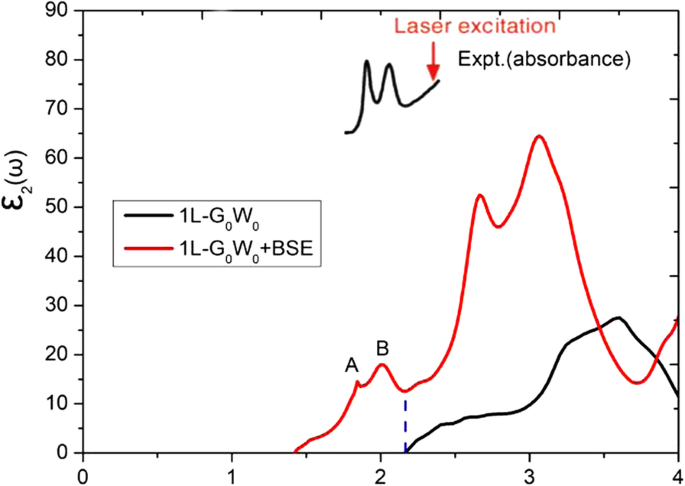
分别使用 G0W0 和 G0W0+BSE 方法得到单层 MoS2 介电函数的虚部。 MoS2 的实验吸收光谱是从参考文献中提取的。 [4]
结果与讨论
MoS2 多层电子结构
结晶二硫化钼天然存在,具有三种结晶类型:1T , 2H , 和 3R ,分别对应于具有三角、六边形和菱形原始晶胞的晶体 [9]。 2H -MoS2 被认为是最稳定的结构 [10];因此,我们只考虑 2H 在这项工作中的块状 MoS2 类型。散装 2H -MoS2 具有六边形层状结构,由被六个硫原子包围的钼原子层组成,S-Mo-S 薄片相对堆积(如图 2 所示)。 2H 的相邻片材 -MoS2 与弱范德瓦尔斯相互作用弱相关。然后可以很容易地从块体上剥离单层 MoS2。块体 MoS2 的晶格常数计算为 a =b =3.19Å,c =12.41 Å,与 a =b 的报告值一致 =3.18 Å,c =13.83 埃 [18]。单层 MoS2 的优化晶格常数为 a =b =3.19 Å,这与块状 MoS2 一致。如表 1 所示,计算出的 a 中的晶格常数 , b 不同层数的 MoS2 方向相同。 Kumar 等人也报道了这一点。 [19] 晶格常数 (a, b ) 的单层 MoS2 几乎与块体相同。
<图片>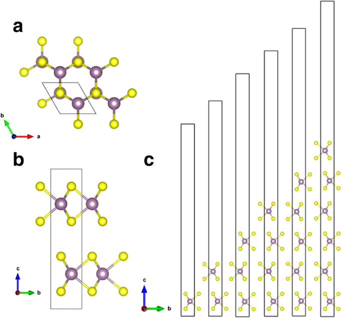
一 顶视图和b 块状二硫化钼的侧视图。 c MoS2 的单层、双层、三层以及四层、五层和六层结构的侧视图。单元格显示在 b 中 .紫色和黄色球分别代表Mo和S原子
图 3 描绘了不同层数的 MoS2 的计算能带结构和电子态密度 (DOS)。图 3 给出了单层、双层、三层和四层以及块状 MoS2 的结果,而五层和六层 MoS2 的结果与四层和块状 MoS2 的结果非常相似。对于单层 MoS2,价带最大值 (VBM) 和导带最小值 (CBM) 均出现在 BZ 的 K 点,直接带隙为 1.64 eV。对于双层和三层 MoS2,两个 VBM 都位于 Γ 点,而两个 CBM 位于 K 点,分别导致 1.17 和 1.08 eV 的间接间隙。然而,随着MoS2层数增加到4层或4层以上,所有多层MoS2都表现出相同的特征,即VBM位于Γ点,而CBM位于Γ和K点之间,这与块体中的相同。四层、五层、六层 MoS2 和块体的间接带隙分别为 1.03 eV、1.01 eV、0.99 eV、0.93 eV。 PBE-D2 和 HSE06 计算(表 1)都表明,当 MoS2 层数减少时,基本带隙单调增加,这是由于板中电子的大量限制 [4, 5, 19, 42]。此外,当块体 MoS2 板减少到单层时,它变成了直接带隙半导体,如前所述,块体 MoS2 是间接带隙半导体。在图 3a 中,块体 MoS2 的能带结构图显示了能带分裂(与单层 MoS2 相比),主要围绕  -point,由于层间耦合 [16]。由于层间耦合,两层 (2L) 和超过 2L MoS2 的能带结构表现出类似的能带分裂。然而,块体中的带分裂比多层 MoS2 中的带分裂更显着,表明块体中的层间耦合(略)强于多层中的层间耦合。另一方面,BZ 中 K 点附近的频带分裂非常小。最高占有能带K点的电子态主要由d组成 xy 和 \( {d}_{x^2-{y}^2} \) Mo 原子的轨道,以及 (p x , p 是 )-S 原子的轨道(如图 4b 所示)。 Mo 原子位于 S-Mo-S 片的中间层,这导致在 K 点的层间耦合可以忽略不计(因为 MoS2 层之间最近的原子是 S 和 S)。如图 4 所示,与 K 点相比,可以发现 Γ 点的层间耦合更强,因为最高占据带的 Γ 点的电子态由 \( {d}_{z^2} \ ) Mo 原子和 p 的轨道 z S 原子的轨道。因此,S-S 耦合(层间耦合)在Γ 点明显强于在K 点。我们的结果与其他理论工作一致[21]。一般而言,少层MoS2的电子态密度与块状MoS2相似(见图3),因为块状MoS2实际上是一种层状材料,MoS2层之间的相互作用较弱。
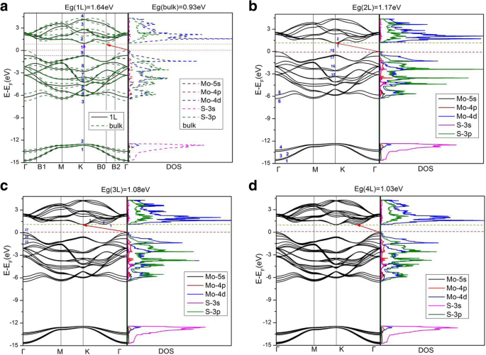
a 的能带结构和态密度计算 单层(实线)和块状(虚线),b 双层,c 三层和d 四层 MoS2。在 a ,在点 K 的体层和单层的最高占据带设置为相同的能量。体的导带最小值在B0点
<图片>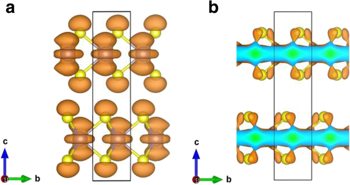
a处最高占据带的电荷分布 观点  和 b 块状 MoS2 的 K 点。等值面值设置为 0.004 e/Å
3
和 b 块状 MoS2 的 K 点。等值面值设置为 0.004 e/Å
3
为了深入探索单层 MoS2 中的键合性质,变形电荷密度如图 5a 所示。变形电荷密度由Δρ给出 1(r ) =ρ (r ) − ∑μ ρ 原子(r − R μ ) 其中 ρ (r ) 是总电荷密度,∑μ ρ 原子(r − R 你 ) 代表独立原子电荷密度的叠加。结果表明,MoS2 单层中的键合以清晰的共价(Mo-S 原子之间的实线轮廓线)以及强离子相互作用(由虚线和实线轮廓的交替区域表示)为特征。为了查看单层 MoS2 与本体中的键合强度,单层和本体 MoS2 之间的电荷密度差异,Δρ 2(r ),也显示在图 5b 中。电荷密度差定义为Δρ 2(r ) =ρ 1L (r ) − ρ 批量(r ),其中 ρ 1L (r ) 和 ρ 批量(r ) 分别是单层和块状 MoS2 的总电荷密度。图 5b 表明单层情况下的电子结合比本体中的电子结合更强,这反映在单层中 Mo-S 原子之间更大的电荷积累(实线等高线),以及在单层中更强的离子键单层 MoS2,因为图 5b 中虚线和实线轮廓的交替区域比块体中的更重要。此外,电荷差异图(图 5b)表明单层的 Mo 原子比体中的 Mo 原子失去更多的电子;因此,单层的离子性强于体层。然而,需要指出的是,图5b中电荷差异的数量级相当小(图5b中的等值线间隔仅为2.5×10 -4 e/Å 3 )。再次从量子限域效应判断,单层的层内相互作用应该强于体层。因此,预计单层的带隙 (1.64 eV) 大于体层 (0.93 eV)。量子限制随着层数的增加而降低[4, 42],这增强了层间耦合并减少了层内相互作用。因此,MoS2 的带隙随着层间耦合的增加而减小。双层 MoS2 的层间电荷密度重新分布,Δρ 3(r ),也呈现在图 5c 中。 Δρ 3(r ) 由 Δρ 给出 3(r ) =ρ 2L (r ) − ρ layer1(r ) − ρ layer2(r ),其中 ρ 2L (r ), ρ layer1(r ), ρ layer2(r ) 分别是双层 MoS2、第一层双层 MoS2 和第二层双层 MoS2 的电荷密度。双层MoS2的layer1和layer2的电荷密度通过使用双层MoS2中的相应结构计算。从 MoS2 层(双层)到 MoS2 层之间的中间区域的电荷转移在图 5c 中清晰可见,显示为实线等高线。从虚线和实线轮廓的交替区域可以看出,双层 MoS2 中原子层之间的离子相互作用也很清楚。同样,层间电荷密度的数量级,Δρ 3(r ),非常小(等高线间隔只有 2.5 × 10 -4 e/Å 3 )。一般来说,2L、3L、……、体MoS2体系的层间电荷密度重新分布都非常相似。
<图片>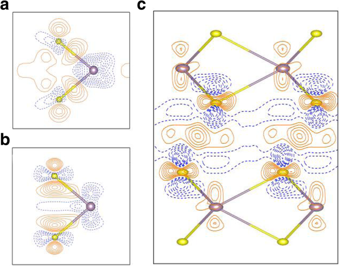
一 变形电荷密度,Δρ 1(r ) =ρ (r ) − ∑μ ρ 原子(r − R μ ),在单层 MoS2 中。 b 单层的电荷密度与相应的体层之间的差异。 c 双层 MoS2 的层间电荷密度重新分布。 a 的轮廓间隔 是 2.5 × 10 −2 e/Å 3 , 而 b 和 c 是 2.5 × 10 −4 e/Å 3 .橙色实线和蓝色虚线对应于 Δρ> 0 和 Δρ <0,分别
二硫化钼多层膜的光学特性
一旦获得材料的基态电子结构,就可以研究其光学特性。介电函数的虚部 \( {\varepsilon}_2^{\alpha \beta}\left(\omega \right) \) 由下式 [43] 确定:
$$ {\displaystyle \begin{array}{c}{\varepsilon}_2^{\alpha \beta}\left(\omega \right)=\frac{4{\pi}^2{e}^2} {\Omega}{\lim}_{q\to 0}\frac{1}{q^2}\underset{c,v,k}{\Sigma}2{w}_k\delta \left({E }_{ck}-{E}_{vk}-\mathrm{\hslash}\omega \right)\\ {}\times \left\lange {u}_{ck+{e}_{\alpha }q }|{u}_{vk}\right\rangle \left\langle {u}_{ck+{e}_{\beta }q}|{u}_{vk}\right\rangle \ast \end{数组}} $$ (1)其中指数 α 和 β 表示笛卡尔方向,c 和 v 参考导带和价带,E ck 和 E vk 分别是导带和价带的能量。 Kramers-Kronig 反演可用于获取由虚部 \( {\ varepsilon}_2^{\alpha \beta}\left(\omega \right) \):
$$ {\varepsilon}_1^{\alpha \beta}\left(\omega \right)=1+\frac{2}{\pi }P{\int}_0^{\infty}\frac{\varepsilon_2 ^{\alpha \beta}\left(\omega \hbox{'}\right)\omega \hbox{'}}{\omega {\hbox{'}}^2-{\omega}^2+ i\ eta} d\omega \hbox{'} $$ (2)其中 P 代表主值。由于 MoS2 具有单轴结构,ε xx (ω ) 那么与 ε 相同 yy (ω )。在这项工作中,我们只需要讨论电矢量 E 与 x-y 平行 平面,即 E|| x 平行于 MoS2 x-y 飞机。
为了研究 MoS2 系统的详细光谱,吸收系数 α (ω ) 和反射率 R (ω ) 由实部 ε 计算 1(ω ) 和虚部  介电函数。提及的参数方程如下:
如果矩阵元素 \( \left\langle {u}_{ck+{e}_{\alpha }q}|{u}_{vk}\right\rangle \) 变化非常缓慢,为 k -vector,术语 \( \left\langle {u}_{ck+{e}_{\alpha }q}|{u}_{vk}\right\rangle \left\langle {u}_{ck+{ e}_{\beta }q}|{u}_{vk}\right\rangle \ast \) 在方程中。 (1) 可取外求和。在方程式中。 (1), \( {\varepsilon}_2^{\alpha \beta}\left(\omega \right) \) 的大部分离散是由于对delta函数δ的求和 (E ck − E vk − ℏω )。通过定义联合态密度 (JDOS) [25, 44],
$$ {J}_{cv}\left(\omega \right)=\frac{1}{4{\pi}^3}\int \frac{dS_k}{\nabla_k\left({E}_{ ck}-{E}_{vk}\right)} $$ (5)其中 ℏω 等于 E ck − E vk , S k 表示由 E 表示的恒定能量表面 ck − E vk =ℏω =常数。状态的联合密度J 简历 (ω ) 与从价带到导带的跃迁以及 J 中的大峰有关 简历 (ω ) 将起源于 ∇k (E ck − E vk ) ≈ 0. k 中的点 -空间其中∇k (E ck − E vk ) =0 称为临界点或范霍夫奇点 (VHS),而 E ck − E vk 被称为临界点能量 [26, 27]。临界点∇k E ck =∇k E vk =0 通常只出现在高对称点,而临界点 ∇k E ck =∇k E vk ≠ 0 可能出现在布里渊区的任何一般点 [27, 45]。在二维情况下,存在三种类型的临界点,即P 0(最低点),P 1(鞍点)和 P 2(最高点)。在点 P 0 或 P 2、JDOS中出现阶跃函数奇点,而在鞍点P 1,JDOS 被描述为对数奇点 [27]。更详细地说,E c (k x , k 是 ) − E v (k x , k 是 ) 可以在关于临界点的泰勒级数中展开。将展开限制为二次项,由于奇点的性质不出现线性项,则有
$$ {E}_c\left({k}_x,{k}_y\right)-{E}_v\left({k}_x,{k}_y\right)={E}_0+\frac{\ mathrm{\hslash}}{2}\left({b}_x\frac{k_x^2}{m_x}+{b}_y\frac{k_y^2}{m_y}\right) $$ (6)因此,出现了三种类型的临界点。对于 P 0, (b x> 0, b 是> 0),对于 P 1, (b x> 0, b 是 <0) 或 (b x <0, b 是> 0),对于 P 2, (b x <0, b 是 <0)。在本文中,对于 MoS2 多层膜,只有 P 0个临界点。
图 6a 给出了 E 的 MoS2 多层介电函数的虚部,\( {\varepsilon}_2^{xx}\left(\omega \right) \) ||x.我们发现了一个有趣的现象,介电函数的虚部\( {\varepsilon}_2^{xx}\left(\omega \right) \) 具有高原,并且不同层MoS2 的高原在范围内几乎相等1.75 eV~2.19 eV。从阈值能量到 1.75 eV,\( {\varepsilon}_2^{xx}\left(\omega \right) \) 对于不同的 MoS2 多层有很大不同。不同层的平台的阈值和结束能量不同,尤其是单层\( {\varepsilon}_2^{xx}\left(\omega \right) \) 平台的能量范围明显宽于那些其他多层。单层 MoS2 介电函数的阈值能量等于其 1.64 eV 的直接带隙。然而,双层介电函数的阈值能量不是1.17 eV的间接带隙,而是价带和导带之间1.62 eV的直接带隙的最小值。这是因为我们只研究了具有相同电子波矢量的价带和导带之间的跃迁,这些跃迁被归类为直接光学跃迁 [36, 47]。随着 MoS2 层数增加到 4,我们发现多层 MoS2 系统的 \( {\varepsilon}_2^{xx}\left(\omega \right) \) 几乎与体相无法区分。因此,我们在此仅详细讨论单层、双层和三层以及块状 MoS2 的平台。单层、双层、三层和块状 MoS2 的 \( {\varepsilon}_2^{xx}\left(\omega \right) \) 平台分别以 2.57 eV、2.28 eV、2.21 eV 和 2.19 eV 结束。为了更准确地解释这一点,图 7 中显示了单层、双层、三层和块状 MoS2 的 JDOS。从图 7 中,平台也显示在 JDOS 中。单层、双层和三层 JDOS 的平台分别以 2.57 eV、2.28 eV、2.21 eV 结束,与它们的 \( {\varepsilon}_2^{xx}\left(\omega \right ) \)对于块体 MoS2,JDOS 的平台期结束于 2.09 eV,略小于介电函数中的 2.19 eV \( {\varepsilon}_2^{xx}\left(\omega \right) \).
<图片>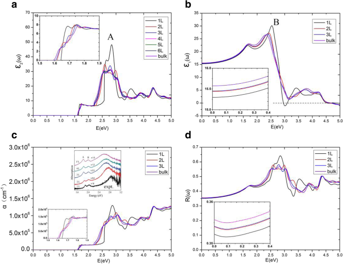
一 介电函数的虚部,b 介电函数的实部,c 吸收系数和 d 不同数量的 MoS2 层的反射率光谱。 c 中的插图 还展示了实验数据 [46]
<图片>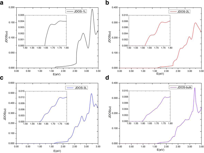
单层、双层、三层和块状 MoS2 的联合态密度
为了准确分析电子跃迁并详细分析介电函数 \( {\varepsilon}_2^{xx}\left(\omega \right) \),直接能隙 ΔE(NC − NV),在单层、双层、三层和块状 MoS2 的导带和价带如图 8 所示。符号 NC 和 NV 表示导带和价带的序数。因此,NC =1、2 和 3 表示材料的最低、第二低和第三低的未占用带。另一方面,NV =9、18 和 27(取决于晶胞中的电子数)分别表示单层、双层和三层 MoS2 的最高占据带。对于单层,在 0 ~ 2.57 eV 范围内,发现电子跃迁仅从最高占据带 NV =9 到最低未占据带 NC =1。从图 8a 中,出现最小值出现在高对称点K 和 JDOS 的阈值(图 7a)出现在 1.64 eV,这实际上是单层 MoS2 的直接带隙。在高对称点K附近,ΔE(NC =1 − NV =9)的曲线类似于单层MoS2的抛物线。因此,∇k (E ck − E vk ) =0 在 K 点,表示高对称点 K 处的临界点。在二维结构中,该临界点属于 P 0 型奇点 [27],因此它导致了 JDOS 中的一个步骤。因此,在临界点能量 1.64 eV 处发现了 JDOS 平台的阈值能量。 JDOS 平台的结束能量接近 2.57 eV,这是由于两个 P 的出现 B1 点处的 0 型奇点 (k =(0.00, 0.16, 0.00)) 和点 B2 (k =(- 0.10, 0.20, 0.00))。 ΔE(NC =1 − NV =9) 曲线在两个临界点 B1 和 B2 附近的斜率非常小,这导致 JDOS 的快速增加(见方程(5))。 JDOS 的这些长平台的主要临界点列于表 2 中,包括类型、位置、过渡带和直接能隙 ΔE(NC − NV)。此外,我们发现 ∇k E ck =∇k E vk =0 发生在高对称点 K 处,其中价带和导带的斜率是水平的。而 ∇k E ck =∇k E vk ≠ 0 发生在 B1 和 B2 点,这意味着两个波段的斜率是平行的。同时,对单层的能带结构和直接能隙(见图8a)的分析表明,当直接能隙ΔE低于2.65 eV时,只有NV =9和NC =1之间的跃迁对JDOS有贡献;当 ΔE 大于 2.65 eV 时,NV =9 到 NC =2 的转变也开始对 JDOS 做出贡献;而当 ΔE 达到 2.86 eV 以上时,NV =9 到 NC =3 的转变对 JDOS 有影响。应该指出的是,对于大于 2.65 eV 的能量,图 8a 中的许多波段将有助于 JDOS。单层 MoS2 的 JDOS 在 1.64 ~ 2.57 eV 范围内呈现平稳状态,并且表达式 |Mvc| 2 /ω 2 发现在这个范围内很小。根据方程。 (1)和(5),介电函数的虚部\( {\varepsilon}_2^{xx}\left(\omega \right) \) 主要由JDOS和过渡矩阵元素决定,这给与 JDOS 相比,介电函数的虚部 \( {\varepsilon}_2^{xx}\left(\omega \right) \) 具有类似的平台。
<图片>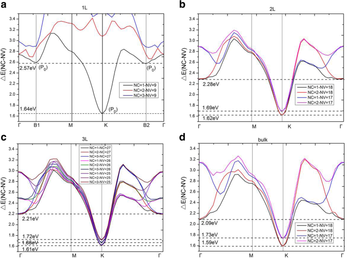
a 导带和价带之间的直接能隙ΔE(NC − NV) 单层,b 双层,c 三层和d 块状 MoS2。 一 –d 单层、双层、三层和块状 MoS2 的带间跃迁分别有 3、6、12 和 6 个临界点
对于双层 MoS2,在 0 ~ 2.28 eV(JDOS 平台的终点)范围内,电子跃迁有助于 NV =17, 18 到 NC =1, 2。ΔE(NC − NV) 中的最小能量位于在 K 点,间隙为 1.62 eV。在图 8b 中,类似于单层 MoS2,双层 MoS2 在 K 点保持两条向上的抛物线曲线(来自 ΔE(NC =1 − NV =18) 和 ΔE(NC =2 − NV =18))。因此,有两个 P 0 型奇点 (∇k (E ck − E vk ) =0) 在 K 点,导致 JDOS 中的一个步骤。 The critical point energies are both 1.62 eV, this is because that the conduction bands (NC =1 and NC =2) are degenerate at point K (as shown in Fig. 3b), which results in the same direct energy gap between transitions of NV =18 to NC =1 and NV =18 to NC =2. From Fig. 8b, as the direct energy gap is increased to 1.69 eV, two new parabolas (which come from ΔE(NC = 1 − NV = 17) and ΔE(NC = 2 − NV = 17)) appear and two new singularities emerge again at K point in the direct energy gap graph, leading to a new step in JDOS for bilayer MoS2 (see Fig. 7b). As a result, the JDOS of the bilayer MoS2 has two steps around the threshold of long plateau (see inset in Fig. 7b). Two parabolas (in Fig. 8b) contribute to the first step and four parabolas contribute to the second step in JDOS. It means that the value of the second step is roughly the double of the first one. As the ΔE reaches to 2.28eV, two new singularities appear at Γ point (where interband transitions come from Γ(NV =18→NC =1) and Γ(NV =18→NC =2)), which have great contribution to the JDOS and bring the end to the plateau. Our calculations demonstrate that ∇k E ck = ∇k E vk = 0 are satisfied not only at high symmetry point K, but also at high symmetry point Γ. Similar to the case of monolayer, we found that the term of |Mvc| 2 /ω 2 is a slowly varying function in the energy range of bilayer JDOS plateau; hence, \( {\varepsilon}_2^{xx}\left(\omega \right) \) of bilayer have a similar plateau in the energy range.
For trilayer MoS2, in the region of 0 ~ 2.21 eV, the JDOS are contributed from electronic transitions of NV =25, 26, and 27 to NC =1, 2, and 3. As shown in Fig. 8c, trilayer MoS2 have nine singularities at three different energies (ΔE =1.61 eV, 1.66 eV, and 1.72 eV, respectively) at the K point. Figure 3c depicts that the conduction bands (NC =1, 2, 3) are three-hold degenerate at point K; this means that there are three singularities at each critical point energy. According to our previous analysis, the JDOS and \( {\varepsilon}_2^{xx}\left(\omega \right) \) of trilayer MoS2 will show three steps near the thresholds of the long plateaus, the endpoints of the long plateaus of trilayer JDOS, and \( {\varepsilon}_2^{xx}\left(\omega \right) \) are then owing to the appearance of three singularities at Γ point with ΔE =2.21 eV (see Fig. 7c), which come from the interband transitions of Γ(NV =27→NC =1, 2, 3).
For bulk MoS2, the thresholds of \( {\varepsilon}_2^{xx}\left(\omega \right) \) and JDOS are also located at K point, with the smallest ΔE(NC − NV) equals to 1.59 eV. Nevertheless, there is no obvious step appeared in the thresholds of plateaus for both the \( {\varepsilon}_2^{xx}\left(\omega \right) \) and JDOS (see Fig. 6a and Fig. 7d). Based on the previous analysis, the number of steps in the monolayer, bilayer, and trilayer MoS2 are 1, 2, and 3, respectively. As the number of MoS2 layers increases, the number of steps also increases in the vicinity of the threshold energy. Thus, in the bulk MoS2, the JDOS curve is composed of numerous small steps around the threshold energy of the long plateau, and finally the small steps disappear near the threshold energy since the width of the small steps decreases. In the region of 0 ~ 2.09 eV, the electron transitions of bulk MoS2 are contributed to NV =17, 18 to NC =1, 2. The 2.09 eV is the endpoint of JDOS plateau of bulk MoS2, which is attributed to two singularities, i.e., the interband transitions of Γ(NV =18→NC =1) as well as Γ(NV =18→NC =2), as presented in Fig. 8d. However, the plateau endpoint of the imaginary part of dielectric function \( {\varepsilon}_2^{xx}\left(\omega \right) \) is 2.19 eV, which is greater than the counterpart of JDOS (e.g., 2.09 eV). Checked the transition matrix elements, it verified that some transitions are forbidden by the selection rule in the range of 2.09 eV to 2.19 eV. Therefore, the imaginary part of the dielectric function \( {\varepsilon}_2^{xx}\left(\omega \right) \) is nearly invariable in the range of 2.09 ~ 2.19 eV. As a result, the plateau of \( {\varepsilon}_2^{xx}\left(\omega \right) \) of bulk MoS2 is then 1.59 ~ 2.19 eV.
It has been shown that these thresholds of the JDOS plateaus are determined by singularities at the K point for all of the studied materials, see Fig. 8. The endpoint energy of the monolayer JDOS plateau is determined by two critical points at B1 and B2 (Fig. 8a). Nevertheless, the endpoint energies of bilayer, trilayer, and bulk JDOS plateaus are all dependent on the critical points at Γ(Fig. 8b–d). The interlayer coupling near point Γ is significantly larger than the near point K for all the systems of multilayer MoS2. The smallest direct energy gap decreases and the interlayer coupling increases as the number of layers grow. With the layer number increases, a very small decrease of direct energy gap at point K and a more significant decrease of direct energy gap at point Γ can be observed, as a result, a faint red shift in the threshold energy and a bright red shift in the end of both JDOS and \( {\varepsilon}_2^{xx}\left(\omega \right) \) plateaus can also be found. For monolayer MoS2, the smallest ΔE(NC − NV) at point Γ is 2.75 eV which is larger than that at point B1 (or point B2) with a value around 2.57 eV. When it goes to multilayer and bulk MoS2, the strong interlayer coupling near point Γ makes the smallest ΔE(NC − NV) at Γ less than those at point B1 (or point B2). Hence, monolayer owns the longest plateau of JDOS, which is between 1.64 eV and 2.57 eV. The shortest plateau of JDOS (from 1.59 eV to 2.09 eV) is shown in the bulk.
As the energy is increased to the value larger than the endpoint of long platform of the dielectric function, a peak A can be found at the position around 2.8 eV, for almost all the studied materials (Fig. 6a). The width of peak A for monolayer is narrower compared with those of multilayer MoS2; however, the intensity of peak A for monolayer is found to be a little stronger than multilayers. The differences between the imaginary parts of dielectric function for the monolayer and multilayer MoS2 are evident, on the other hand, the differences are small for multilayer MoS2.
In order to explore the detailed optical spectra of MoS2 multilayers, the real parts of the dielectric function ε 1(ω ), the absorption coefficients α (ω ), and the reflectivity spectra R (ω ) are presented in Fig. 6b–d. Our calculated data of bulk MoS2 for the real and imaginary parts of the dielectric function, ε 1(ω ) 和 ε 2(ω ), the absorption coefficient α (ω ) and the reflectivity R (ω ) agree well with the experimental data, except for the excitonic features near the band edge [48,49,50]. The calculated values of  , which is called the static dielectric constant, for MoS2 multilayers and bulk can be found in Table 1. From Table 1, the calculated values of \( {\varepsilon}_1^{xx}(0) \) for multilayers and bulk MoS2 are all around 15.5, which is very close to the experimental value of 15.0 for bulk MoS2 [50]. The values of \( {\varepsilon}_1^{xx}(0) \) increase with the increasing number of MoS2 layers. For monolayer MoS2, a clear peak B of \( {\varepsilon}_1^{xx}\left(\omega \right) \) appears about 2.54 eV. Peak B of monolayer is clearly more significant than multilayers, and they are all similar for multilayer MoS2. As the layer number increases, the sharp structures (peak B) also move left slightly. In Fig. 6c, we also observe the emergence of long plateaus in the absorption coefficients, and absorption coefficients are around 1.5 × 10
5
cm
−1
at the long plateaus. There are also small steps around the thresholds for the absorption coefficients, which are consistent to those of the imaginary parts of dielectric function. With the layer number increases, the threshold energy of absorption coefficient decreases, while the number of small steps increases at the starting point of the plateau. For monolayer and multilayer MoS2, strong absorption peaks emerge at visible light range (1.65–3.26 eV), and the monolayer MoS2 own a highest absorption coefficient of 1.3 × 10
6
cm
−1
. The theoretical absorption coefficients for different number of MoS2 layers are compared with confocal absorption spectral imaging of MoS2 (the inset) [46], as shown in Fig. 6c. For monolayer and multilayer MoS2, a large peak of α (ω ) can be found at the position around 2.8 eV for both the calculation and experiment [46, 51]. Furthermore, a smoothly increase of α (ω ) can be found between 2.2 and 2.8 eV for both the theoretical and experimental curves. Therefore, from Fig. 6c, the calculated absorption coefficients of MoS2 multilayers show fairly good agreement with the experimental data [46], except for the excitonic peaks. The reflectivity spectra are given in Fig. 6d. The reflectivity spectra of MoS2 multilayers are all about 0.35–0.36 when energy is zero, which means that MoS2 system can reflect about 35 to 36% of the incident light. In the region of visible light, the maximum reflectivity of monolayer MoS2 is 64%, while the maxima of multilayer and bulk MoS2 are all about 58%. Because of the behaviors discussed, MoS2 monolayer and multilayers are being considered for photovoltaic applications.
, which is called the static dielectric constant, for MoS2 multilayers and bulk can be found in Table 1. From Table 1, the calculated values of \( {\varepsilon}_1^{xx}(0) \) for multilayers and bulk MoS2 are all around 15.5, which is very close to the experimental value of 15.0 for bulk MoS2 [50]. The values of \( {\varepsilon}_1^{xx}(0) \) increase with the increasing number of MoS2 layers. For monolayer MoS2, a clear peak B of \( {\varepsilon}_1^{xx}\left(\omega \right) \) appears about 2.54 eV. Peak B of monolayer is clearly more significant than multilayers, and they are all similar for multilayer MoS2. As the layer number increases, the sharp structures (peak B) also move left slightly. In Fig. 6c, we also observe the emergence of long plateaus in the absorption coefficients, and absorption coefficients are around 1.5 × 10
5
cm
−1
at the long plateaus. There are also small steps around the thresholds for the absorption coefficients, which are consistent to those of the imaginary parts of dielectric function. With the layer number increases, the threshold energy of absorption coefficient decreases, while the number of small steps increases at the starting point of the plateau. For monolayer and multilayer MoS2, strong absorption peaks emerge at visible light range (1.65–3.26 eV), and the monolayer MoS2 own a highest absorption coefficient of 1.3 × 10
6
cm
−1
. The theoretical absorption coefficients for different number of MoS2 layers are compared with confocal absorption spectral imaging of MoS2 (the inset) [46], as shown in Fig. 6c. For monolayer and multilayer MoS2, a large peak of α (ω ) can be found at the position around 2.8 eV for both the calculation and experiment [46, 51]. Furthermore, a smoothly increase of α (ω ) can be found between 2.2 and 2.8 eV for both the theoretical and experimental curves. Therefore, from Fig. 6c, the calculated absorption coefficients of MoS2 multilayers show fairly good agreement with the experimental data [46], except for the excitonic peaks. The reflectivity spectra are given in Fig. 6d. The reflectivity spectra of MoS2 multilayers are all about 0.35–0.36 when energy is zero, which means that MoS2 system can reflect about 35 to 36% of the incident light. In the region of visible light, the maximum reflectivity of monolayer MoS2 is 64%, while the maxima of multilayer and bulk MoS2 are all about 58%. Because of the behaviors discussed, MoS2 monolayer and multilayers are being considered for photovoltaic applications.
结论
In this study, by employing ab initio calculations, the electronic and optical properties of MoS2 multilayers are investigated. Compared to bulk MoS2, the covalency and ionicity of monolayer MoS2 are found to be stronger, which results from larger quantum confinement in the monolayer. With the increase of the layer number, quantum confinement and intra-layer interaction both decrease, meanwhile, the interlayer coupling increases, which result in the decrease of the band gap and the minimum direct energy gap. As the layer number becomes larger than two, the optical and electronic properties of MoS2 multilayers start to exhibit those of bulk. Band structures of multilayers and bulk show splitting of bands mainly around the Γ-point; however, splitting of bands in the vicinity of K point are tiny, owing to the small interlayer coupling at point K.
For optical properties, Van Hove singularities lead to the occurrence of long plateaus in both JDOS and \( {\varepsilon}_2^{xx}\left(\omega \right) \). At the beginnings of these long plateaus, monolayer, bilayer, and trilayer structures appear one, two, and three small steps, respectively. With the layer number increases, the number of small steps increases and the width of the small steps decreases, leading to unobvious steps. A small red shift in the threshold energy and a noticeable red shift in the end of both JDOS and \( {\varepsilon}_2^{xx}\left(\omega \right) \) plateaus are observed, since the increased number of layers leads to small changes in the direct energy gap near point K (weak interlayer coupling) and larger changes near point Γ (stronger interlayer coupling). Thus, the longest plateau and shortest plateau of JDOS are from the monolayer and bulk, respectively. Our results demonstrate that the differences between electronic and optical properties for monolayer and multilayer MoS2 are significant; however, the differences are not obvious between the multilayer MoS2. The present data can help understand the properties of different layers of MoS2, which should be important for developing optoelectronic devices.
数据和材料的可用性
The datasets supporting the conclusions of this article are included within the article.
缩写
- Δ E:
-
The direct energy gap
- 1L:
-
Monolayer MoS2
- 2L:
-
Bilayer MoS2
- 3L:
-
Trilayer MoS2
- 4L:
-
Four-layer MoS2
- 5L:
-
Five-layer MoS2
- 6L:
-
Six-layer MoS2
- BSE:
-
Bethe-Salpeter equation
- BZ:
-
Brillouin zone
- CBM:
-
导带最小值
- GGA:
-
广义梯度逼近
- GW:
-
Quasi-particle energy calculation
- JDOS:
-
Joint density of states
- MoS2:
-
二硫化钼
- NC:
-
The ordinal numbers of conduction band
- NV:
-
The ordinal numbers of valence band
- 爪子:
-
投影仪增强波
- PBE:
-
Perdew-Burke-Ernzerhof
- VASP:
-
Vienna ab initio 仿真包
- VBM:
-
价带最大值
- VHS:
-
Van Hove singularity
纳米材料
- 揭示叠杯碳纳米纤维的原子和电子结构
- 过渡金属掺杂高岭石纳米粘土的结构和电子特性
- 垂直电场对 ML-GaS 的电子和光学各向异性特性的调制
- 小型硒纳米晶体和纳米棒的简便合成和光学特性
- 双层厚度对 Al2O3/ZnO 纳米层压材料的形态、光学和电学特性的影响
- 飞秒激光诱导硫超掺杂硅 N+/P 光电二极管的光学和电子特性
- 探测 Ag n V (n =1-12) 簇的结构、电子和磁特性
- 纳米粒子毒性对其物理和化学性质的依赖性
- Al-Doped ZnO 薄膜在红外区域的光学特性及其吸收应用
- 碱金属吸附的 g-GaN 单层:超低功函数和光学特性
- 钒原子在清洁和石墨烯覆盖的 Cu(111) 表面吸附的电子特性
- 基材对 LSP 耦合波长和强度的影响