

具有不同石墨烯谐振器的系统中的两种可切换等离子诱导透明效应
摘要
实现等离子体诱导透明(PIT)效应的一般等离子体系统只存在一个单一的PIT,主要是因为它们只允许一个单一的耦合途径。在这项研究中,我们提出了一种独特的基于石墨烯谐振器的系统,该系统由石墨烯纳米带 (GNR) 与加载介电光栅的石墨烯层谐振器组成,以实现两种可切换的 PIT 效应。通过设计谐振器的交叉方向,所提出的系统存在两种不同的 PIT 效应,其特征在于不同的谐振位置和线宽。这两种 PIT 效应源自两条独立的极化选择性耦合路径,使我们能够通过简单地改变极化方向将 PIT 从一个路径切换到另一个路径。进行参数研究以证明耦合效应,而双粒子模型用于解释物理机制,在数值和理论结果之间找到了极好的一致性。我们的提议可用于设计可切换的基于 PIT 的等离子体器件,例如可调双波段传感器和完美吸收器。
介绍
表面等离子体是在绝缘和导电介质之间的界面处产生的自由电子的集体谐振模式 [1, 2]。由于它们能够将入射电磁场限制在亚波长范围内单原子尺度的极限大小 [3],表面等离子体已成为实现强光物质相互作用的最基本和最重要的方法之一 [4] .在各种类型的等离子体系统中都发现了这种吸引人的光学现象,这有助于开发各种最先进的应用,例如生物传感 [5]、非线性光学 [6, 7]、吸收器 [8,9] ,10,11] 和其他等离子体调制器 [12,13,14,15]。实现这些重要应用的可能性归因于一些有趣的现象,如等离子体诱导透明度 (PIT)。被称为 PIT 的过程是近场耦合 Fano 干涉的结果,其特点是在光谱中产生一个突出的窗口,因为它消除了系统中的共振吸收。在过去的几年中,这种相干等离子体相互作用已被用于实现各种应用,例如等离子体切换[16]、慢光传播[17]和传感[18]以及光存储[19]。
尽管最近的研究表明,低至原子厚度的超薄金属膜可以具有动态电可调性 [20, 21],但这些新型金属支持的等离子体激元仍然遭受金属的相对较大的欧姆和辐射损失 [22, 23]。金属的这些缺点限制了金属负载PIT的进一步发展,需要寻找新的等离子体材料。与金属等离子激元相比,石墨烯(形成对称六边形蜂窝晶格的紧密结构碳原子的单原子层)支持的等离子激元不仅可以通过静电偏置进行连续和动态调谐 [24, 25],而且具有长传播长度,这使得新一代可重构等离子体设备成为可能,因此为实现有源 PIT 提供了理想的平台 [26, 27]。尽管各种材料和设计已被用于在纯金属 [16, 28,29,30,31] 和石墨烯 [32,33,34,35,36,37,38,39,40,41,42] 中实现 PIT ,或者它们的基于混合材料的 [43,44,45] 系统,这些系统中的大多数只能实现单个 PIT 效果。例如,实现 PIT 的常用方法之一是设计 π -形/类似超表面 [16, 28, 30, 33, 37, 45]。另一种方法是构建光栅耦合系统 [32, 34]。然而,这类结构只能实现偏振相关的单窗口 PIT。这是因为,由于这些结构的特殊几何不对称性,所有纳米结构谐振器都预设为以亮(辐射/超辐射)或暗(非辐射/亚辐射)模式运行。因此,它们在一个特定的偏振方向上只允许一条亮到暗的耦合路径,导致只有一种偏振相关的 PIT 效应。尽管我们之前的研究已经证明 PIT 系统在纯石墨烯纳米带 (GNR) [35] 或光栅耦合 [38] 结构中具有两个明暗模式耦合路径,但计数偏振不敏感的单窗口 PIT 或偏振相关的双-这些系统中的窗口 PIT 效应强烈依赖于几何参数的特定选择(参见讨论部分)。
在本文中,我们建议使用两个不同的谐振器,即 GNR 与加载有介电光栅的石墨烯片耦合,以耦合并实现两个独立的 PIT 效应。我们将证明,通过设置垂直谐振方向,在入射光的不同偏振方向下将产生在两个谐振器中谐振的表面等离子体激元,从而导致两个不同的偏振相关耦合路径,从而产生两个独立的 PIT 效应。此外,参数研究将用于详细研究耦合机制。并且将结合先进的模拟和基于双粒子模型的理论分析来展示这些可切换的 PIT 效应。最后,将讨论所提出的系统的潜在应用,例如折射率传感器和完美吸收器,以及与其他 PIT 系统的比较。
设计和材料
在这部分中,我们介绍了本研究中使用的数值模型和相关材料。我们声明,在我们的模型中,我们只考虑经典电动力学,而忽略了可能由 GNR 的量子有限尺寸效应、石墨烯的非线性效应和基底声子效应引起的任何效应 [46]。所提出系统的示意图如图 1 所示。两个石墨烯层放置在 x 上 oy 平面并由折射率 n 的掺杂 Si 或 SiO2 导体隔开 3和厚度d .第一层由下层石墨烯纳米带 (LGNRs) 形成,周期在 x 方向。第二层是一个完整的石墨烯片,它进一步被具有折射率n的介电光栅覆盖 1(标记为上石墨烯光栅,UGG)和周期 P d 在 y 方向。几何参数固定为W r =W d =50 nm, p r =p d =100 nm, h =100 nm 和 d =20 nm,如图 1 所示。石墨烯层周围的其他材料的介电常数设置为 n 0 和 n 2,如图1所示。为简单起见,不失一般性,假设介电常数为n 1 =2.0 和 n 0 =n 2 =n 3 =1.0。忽略折射率的虚部不会改变本研究的基本结论。请注意,除非另有说明,否则上述参数保持不变。在技术上,使用成熟的图案化和光栅技术实现所设计的两层石墨烯基 PIT 系统在实验上是可行的,该技术最近已用于制造层状石墨烯系统 [27, 47]。
<图片>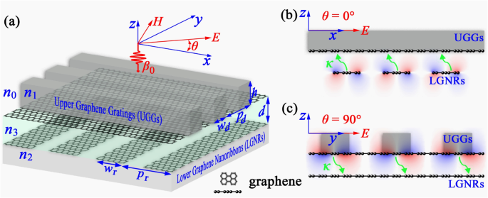
3D (a ) 和二维侧视图 (b , c ) 建议的 PIT 系统。一层加载有周期性介电光栅的石墨烯层覆盖在一层具有交叉光栅和带状方向的周期性 GNR 之上。上层石墨烯光栅层设计有光栅宽度W d , 高度 h , 和横向周期 P d , 而较低的石墨烯纳米带具有带宽度 W r 和期间 P r .两层石墨烯之间的距离为d ,假设其被具有折射率 n 的导电 Si 或 SiO2 间隔物填充 3. 介质光栅及其上方和 GNR 下方的折射率标记为 n 1、n 0 和 n 2、分别。波数为β的线偏振平面波 0 和偏振角θ 关于 x -轴通常撞击层状石墨烯系统的表面
方法
通过使用基于 Lumerical FDTD 解决方案的有限差分时域 (FDTD) 方法对所提出的结构进行数值模拟。在我们的模拟中,在 x 和 y 方向都使用了周期性边界条件。宽带平面波从 z 方向入射,沿 z 方向应用完美匹配的层以吸收所有到达边界的光。电场分布由 2D 场分布监视器在谐振波长处收集,两层之间距离石墨烯表面 0.5 nm。此外,石墨烯薄膜在随机相位近似 (RPA) [48, 49] 中进行了描述。在这个近似值内,面内光导率 σ 石墨烯在中红外范围内写成半经典德鲁德式表达式为 σ (ω ) =即 2 E F /[πћ 2 (ω + iτ −1 )] [24, 50]。在这里,E F =ћν F (n g π ) 1/2 是石墨烯的费米能级,n g = (μ/ћν F ) 2 /π 是载流子浓度(其中 μ =15,000 cm 2 /(V × s ) 是测得的直流迁移率,ν F =10 6 m/s 是费米速度,ћ 是减少的普朗克常数)并且可以通过电门控进行调整 [24, 25, 50], ω 是角频率,τ =μE F / (ev F 2 ) 是载流子弛豫时间。在本文中,E F 除非另有说明,否则固定为 0.6 eV。在我们的模拟中,石墨烯的光学特性是通过使用各向异性相对介电常数张量来描述的 [35]。 z 石墨烯介电常数分量设为ε zz =2.5 基于石墨的介电常数,而面内分量为 ε xx =ε yy =2.5 + iσ (ω )/(ε 0ωt ) [24, 51], 与 ε 0 是真空介电常数,t =1 nm 为石墨烯的厚度[35]。
通过在 x 中应用双粒子模型 和 y 轴,我们可以通过以下方程组[8, 52, 53]从理论上分析图1所示的有效等离子体共振和耦合:
$$ {a}_{1i}^{{\prime\prime} }(t)+{\gamma}_{1i}{a}_{1i}^{\prime }(t)+{\omega} _{1i}^2{a}_{1i}(t)+{\kappa}_{12i}^2{a}_{2i}(t)={Q}_{1i}E\sin \theta /{m}_{1i} $$ (1) $$ {a}_{2i}^{{\prime\prime} }(t)+{\gamma}_{2i}{a}_{2i} ^{\prime }(t)+{\omega}_{2i}^2{a}_{2i}(t)+{\kappa}_{21i}^2{a}_{1i}(t) ={Q}_{2i}E\cos \theta /{m}_{2i} $$ (2)其中 i =x 或 y; γ 我 是损耗因子,与频谱线宽有关; ω 我 是谐振器的谐振频率; 问 我 是模式的有效电荷,它显示了共振模式的强度;和 m 我 是相应共振方向的粒子的有效质量。 κ 我 是 i 中两层之间的耦合强度 方向对应于两种耦合模式的电子-电子相互作用,因此由等离子体的特殊场分布和谐振器之间的耦合距离决定。考虑到等离子体耦合仅沿两个坐标轴,耦合强度为κ 12i =κ 21i =κ 我 ,我们可以将系统视为在不同方向独立谐振的两组独立谐振器。我们假设所有粒子都与入射电场 E 耦合 =E 0e iωt , 生成位移向量 a 我 =c 我 e iωt .在对方程进行一些代数计算之后。 (1)和(2),等离子体的模幅可以表示为:
$$ {a}_{1i}(t)=\frac{\kappa_i^2{Q}_{2i}E\cos \theta /{m}_{2i}+\left({\omega}^2 -i{\omega \gamma}_{2i}-{\omega}_{2i}^2\right){Q}_{1i}E\sin \theta /{m}_{1i}}{\kappa_i ^4-\left({\omega}^2-i{\omega \gamma}_{1i}-{\omega}_{1i}^2\right)\left({\omega}^2-i{ \omega \gamma}_{2i}-{\omega}_{2i}^2\right)} $$ (3) $$ {a}_{2i}(t)=\frac{\kappa_i^2{ Q}_{1i}E\sin \theta /{m}_{1i}+\left({\omega}^2-i{\omega \gamma}_{1i}-{\omega}_{1i} ^2\right){Q}_{2i}E\cos \theta /{m}_{2i}}{\kappa_i^4-\left({\omega}^2-i{\omega \gamma}_ {1i}-{\omega}_{1i}^2\right)\left({\omega}^2-i{\omega \gamma}_{2i}-{\omega}_{2i}^2\对)} $$ (4)有效电化率 (χ eff),表示总极化率 (P ) 和入射电场的强度,则可以用位移矢量的形式表示为:
$$ {\displaystyle \begin{array}{c}{\chi}_{e\mathrm{ff},i}=\frac{P_i^2}{\varepsilon_0E}=\frac{Q_{1i}{a }_{1i}+{Q}_{2i}{a}_{2i}}{\varepsilon_0E}\\ {}=\frac{\left[{\kappa}_i^2{Q}_{1i} {Q}_{2i}+\left({\omega}^2-i{\omega \gamma}_{2i}-{\omega}_{2i}^2\right){Q}_{1i} ^2\right]\sin \theta /{m}_{1i}+\left[{\kappa}_i^2{Q}_{1i}{Q}_{2i}+\left({\omega} ^2-i{\omega \gamma}_{1i}-{\omega}_{1i}^2\right){Q}_{2i}^2\right]\cos \theta /{m}_{ 2i}}{\varepsilon_0\left[{\kappa}_i^4-\left({\omega}^2-i{\omega \gamma}_{1i}-{\omega}_{1i}^2\ right)\left({\omega}^2-i{\omega \gamma}_{2i}-{\omega}_{2i}^2\right)\right]}\end{array}} $$ ( 5)然后,可以通过磁化率的虚部拟合模拟的透射和吸收光谱。在本文中,吸收定义为A =Im[χ 效果,i ]。该系数来自能量守恒关系T + A =1;因此,我们有传输 T 的表达式 =1 - Im[χ 效果,i ].
结果
PIT 效应的激发
为了激发PIT效应,需要解决的一个问题是如何设计亮模谐振器。由于进入的自由空间波和等离子体波之间的大动量不匹配,等离子体的激发是石墨烯等离子体使用的主要挑战之一。为了结束这一点,已经提出并在理论上和实验上证明了几种能够激发石墨烯等离子体的方法。第一种常用的方法是将石墨烯单层图案化为共面纳米结构,例如纳米带 [25, 54]、纳米盘 [55, 56] 和圆形 [24]。另一种方法是在连续的石墨烯片中构建光栅配置,这可以通过使用衍射介质光栅 [51, 57] 和电场门 [58] 来构建位置相关的周期性局部电导率光栅或使用周期性衍射来实现。由石墨烯片本身形成的波纹光栅 [57, 59]。在这些石墨烯结构中表面等离子体激元可以被激发的原因是纳米结构或光栅可以为等离子体波提供额外的互易波矢,当极化方向沿着周期方向时,这是补偿波矢失配所必需的 [51] , 54, 59]。在这种情况下,石墨烯谐振器可以作为亮模式运行,也可以作为暗模式运行。在这里,我们建议使用 GNR 和加载有矩形介质光栅的石墨烯片分别作为明暗模式来构建 PIT 系统,如图 1 所示。
为了探索所提出的 PIT 系统的机制,计算了图 1 所示配置的数值模拟,两种不同偏振角的相应结果如图 2 所示。对于θ =0°,我们首先计算了下部石墨烯纳米带(LGNRs)和上部介电光栅加载石墨烯单独存在的情况的结果。由于偏振方向垂直于 LGNR,SP 可以在其上被激发,从而在 5.327 μm 处产生主吸收峰,如图 2a 中的蓝线所示。相比之下,上部石墨烯片上的 SP 不能在这种偏振条件下被激发,因为入射光平行于电介质光栅偏振,导致强烈的动量失配,如图 2a 中的扁平绿线所示。在这些情况下,我们将 LGNR 中的直接激发模式和 UGG 中的暗模式分别称为 LGNRs-0 和 UGGs-0,如图 2g 和 f 所示。然而,这里有趣的是,当这两个石墨烯层放在一起并且足够接近时,两个吸收峰(透射下降)出现在 5.747 μm 和 4.917 μm。谐振波长较长的一种吸收率达到47.16%,而谐振波长较短的一种吸收峰为35.88%,表明这两种模式与外部入射光的相互作用非常强烈,如图所示. 2a 并在表 1 中得出结论 这两种模式源自两个谐振器之间的同相和异相等离子体耦合。具体来说,LGNR 上的亮模式共振应被视为固定模式,因为它是由入射光直接激发的。然而,上石墨烯层中的等离子体共振不能直接激发,但可以通过同相和异相相互作用与 LGNR 中激发的共振耦合。正是两个谐振器的共存及其等离子体耦合直接导致了这种 PIT 效应。为了清楚地揭示两种模式起源背后的物理机制,我们在图 2h 和 i 中显示了这两种模式的电场分布。根据E z 在分量场分布中,5.747 μm 处的模式显示出层状结构的同相谐振特性,因此称为对称模式。 4.917 μm 处的模式显示出反相共振,称为反对称模式。此外,图 2h 和 i 清楚地揭示了这些模式的结构:所有的 E z 组件显示偶极子模式共振特征为 2π 沿极化方向的相移 (x 轴)在每个石墨烯层中。这两种基本模式消除了 LGNRs 的共振吸收,同时在光谱中产生了一个突出的透射窗口和两个吸收峰,从而产生了称为 PIT 的光学效应(为了讨论方便,我们称之为 LGNRs-PIT)。在图2c中,我们还绘制了两个吸收峰的透射相位和延迟时间,后者分别达到0.34 ps和0.36 ps,表明系统中的慢光效应。
<图片>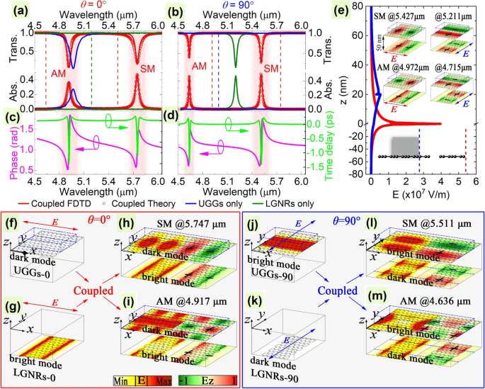
传输线和吸收线 (a , b ) 和它们的传输阶段 (left y 轴)和延迟时间(右 y 轴)(c , d ) 具有偏振角 θ 的系统 =0° (a , c ) 和 90° (b , d ), 分别。在 (a ) 和 (b ),虚线表示另一个极化的谐振位置。 (a中理论分析线的拟合参数 ) 和 (b ) 为(以太赫兹为单位)6.71、110.07、2.25、0.46 和 0.74,以及 κ 的 5.73、4.13、72.83、0.33 和 0.27 我 , 问 1i /sqrt(ε 0米 1i ), 问 2i /sqrt(ε 0米 2i ), γ 1i , 和 γ 2i , 分别。 UGG 情况下的电场空间分布 (e (蓝线),f , j ) 和 LGNR (e (红线),g , k) 仅沿 z 轴 (e ) 和相应的石墨烯平面 (f , g , j , k )。电场的空间分布(左图)和相应的 z 对称模式 (SM) (h , @5.747 μm; 我 , @5.511 μm) 和反对称模式 (AM) (i , @4.917 μm; 米 , @4.636 μm) 在偏振角 θ =0° (h , i ) 和 90° (l , 米 ), 分别。 e 中的上部插入 显示 z d 情况下的电场分量 =50 nm,而下方的插图描绘了主图中场的位置。符号“+”和“-”表示共振表面电荷;颜色越深代表电荷密度越大
而对于θ的情况 =90°,SPs 可以在 UGGs 上被激发,主要吸收峰在 5.202 μm,但当它们单独存在时不能在 LGNRs 上激发,如图 2b 中的绿线和蓝线所示。在这些情况下,我们将 UGG 中的直接激发模式和 LGNR 中的暗模式分别称为 LGNRs-90 和 UGGs-90,如图 2j 和 k 所示。然而,当这两种模式足够接近以相互耦合时,在 5.511 μm 和 4.636 μm 处明显出现两个透射下降(吸收峰),吸收分别达到 49.07% 和 46.46%,这意味着与外部入射波的相互作用非常强,如图2b所示,总结在表1中。类似于θ的情况 =0°,物理机制也可以通过考虑两个石墨烯层之间的同相和异相等离子体耦合来理解。正如图 2l 和 m 清楚地说明的那样,E z 分量场分布显示偶极子模式共振特征为 2π 沿 y 的相移 每个石墨烯层中的轴,并在相应的吸收峰处显示同相(对称模式)和异相(反对称模式)共振。正是这两种基本模式消除了只有UGGs的情况下的共振吸收,同时在光谱中产生了一个突出的透射窗口和两个吸收峰,从而产生了另一个PIT(为了讨论方便,我们称之为UGGs-PIT )。在图2d中,还绘制了两个吸收峰的传输相位和延迟时间,显示了在对称模式和反对称模式下峰值分别为0.23 ps和0.21 ps的减慢光传播效应。
然而,重要的是要注意,尽管图 2i 和 m 中反对称模式的上部石墨烯片中的场分布显示出“多极”谐振外观,但它们仍然是偶极模式,因为电荷振荡也保持了沿极化方向的偶极模式共振。 “多极”谐振出现的原因是来自 LGNR 的强场干扰。这可以通过考虑这样一个事实来理解,即图案化 GNR 中最强的局部等离子体场比连续石墨烯片 [60] 中的更明显,如图 2e 所示。通过将场监视器设置在两个石墨烯层之外或使用大耦合距离,例如当 d 时,这些“多极”模式外观将消失 =50 nm,“多极”模式外观将变为纯偶极模式共振,如图 2e 的插图所示。此外,我们还注意到两个石墨烯层之间的模式耦合是不同的。具体来说,对于θ的情况 =0°,LGNRs-PIT 是 LGNRs-0 和 UGGs-0 之间强耦合的结果,它们沿 x 共振 方向。而对于θ的情况 =90°,UGGs-PIT 是 UGGs-90 和 LGNRs-90 之间强耦合的结果,它们沿 y 共振 方向,如图 2 所示。因此,LGNRs-PIT 和 UGGs-PIT 是在不同极化下谐振的不同模式之间的等离子体耦合效应,导致两种不同的 PIT 效应。
因此,我们可以从图 2 中得出结论,LGNRs-PIT (with θ =0°) 和 UGGs-PIT(带有 θ =90°) 是两种不同的 PIT 效应,它们是由分层石墨烯系统的两个单独的明暗模式耦合路径引起的,并由不同的光谱响应决定。这意味着我们可以通过改变入射光的偏振方向将这两种 PIT 效应从一种切换到另一种,这与偏振不敏感 PIT 效应有很大不同(见讨论部分)。此外,这种可切换的 PIT 效应可以通过等式中所示的双粒子模型来解释。 (1) 和 (2)。对于θ的情况 =0°,UGG 与入射场的直接耦合效率为零(暗),而 LGNR 的直接耦合效率最高(亮),如等式右侧所示。而对于θ的情况 =90°,反之亦然,UGG 变亮而 LGNR 变暗。请注意,在这两种情况下,使用方程获得的分析结果之间的一致性。 (5)(由图 2a、b 中的红色圆圈表示)和数值结果(在图 2a、b 中用红线绘制)几乎是完美的。我们的分析模型不仅非常准确地预测了共振的位置,而且预测了共振的峰值,如图 2 所示。最后,我们注意到这里提供的结果与其他使用相同的谐振器 [35, 38];这是因为他们无法在不同的极化下得到图 2 所示的结果。我们将在讨论部分进一步讨论差异。
PIT 的几何可调性
我们已经证明,亮模式和暗模式之间的近场耦合会导致两种偏振相关的 PIT 效应;因此,显着影响明暗模式共振的参数,以及它们之间的耦合强度,可以被视为 PIT 效果的可调参数。我们首先对 θ 的情况进行参数研究 =0° 通过改变宽度 (W r ) 的 LGNRs 和宽度 (W d ) 的 UGGs 从 20 到 100 nm,结果分别显示在图 3a 和 c 中。由于 LGNR 直接与入射光耦合并在这些条件下作为亮模式工作,因此其尺寸的任何变化都会直接影响系统的整个等离子体响应。例如,当 W r 非常小,例如 20 nm,由于 GNR 的低占有率 [14, 51],与入射光的耦合效率非常弱,导致反对称模式,尤其是 PIT 系统的对称模式吸收率低,从W的吸收线可以看出 r =20 nm 在图 3a 中。再举一个例子,当 W r 足够大,特别是当它达到最大 100 nm 时(即当 LGNRs 是一个完整的石墨烯层时),两个谐振器都不能与外场耦合,因此,LNGRs-PIT 消失了。值得注意的是,当 W 时,两种模式的吸收同时显示出最高值。 r 大约是 50 nm。与亮模式不同,DG宽度(W d ) 在暗模式的上石墨烯层中,只能将谐振位置和对称模式和反对称模式的吸收调整在一定范围内,而不能消除甚至显着影响与外波的高耦合效率,如图 2 所示。 3c。实际上,即使介质光栅被去除或成为整个介质层(W d =100 nm),LGNRs 仍然可以与上层石墨烯片耦合,正如之前工作 [36] 中描述的二维情况所证明的那样,其中只允许存在一个 PIT 效应。
<图片>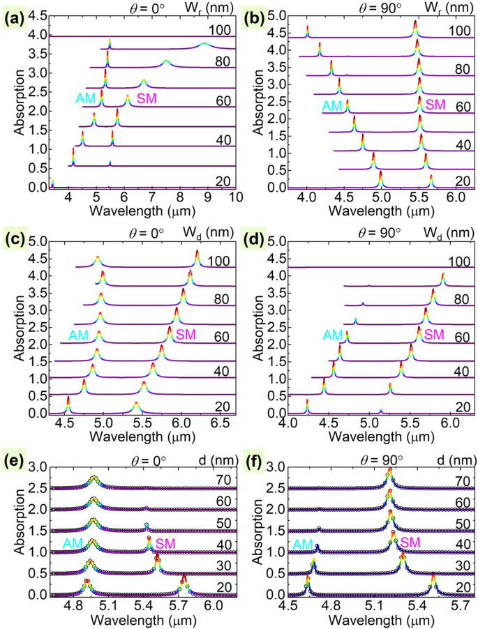
PIT 系统在波长范围内的吸收光谱作为 (a ), (b ) 色带宽度 W r LGNR; (c , d ) DG 宽度 W d 的UGG;和 (e , f ) 间隔距离 d 在偏振角为 θ 的两个石墨烯层之间以 10/20 nm 的步长 =0° (a , c , e ) 和 90° (b , d , f ), 分别。在 (a –f ),实线中的红色越深表示吸收越强。请注意,一些线被切断以避免其他高阶吸收峰的干扰。在 (e ) 和 (f ),实线和黑圈分别表示数值和理论结果。 SM和AM分别是指对称模和反对称模
然而,对于θ的情况 =90°,结果与θ的情况相反 =0° 因为 LGNR 以暗模式工作,而 UGG 以亮模式工作。详细来说,LGNR宽度W的变化 r 仅调制对称模式和反对称模式的共振位置和最大吸收,而不能消除这两种模式的存在,如图 3b 所示。这是因为 LGNR 在这种偏振条件下作为暗模式运行。在带有 W 的条件下 r =100 nm,该系统成为负载 DG 的石墨烯片与另一个石墨烯片耦合,这类似于之前在另一项研究中报道的二维单 PIT 系统 [34]。然而,上部介质光栅的变化将极大地影响 PIT 系统的光学响应,因为在这种情况下上部石墨烯片作为亮模式工作,这与改变 W 时的情况非常相似 r 与 θ =0°,如图 3d 所示。一般来说,我们可以从图 3a-d 中得出结论,明亮模式的调整将极大地影响 UGGs-PIT 的外观甚至存在,如图 3a 和 d 所示,而暗模式只能改变UGGs-PIT中对称模式和反对称模式的共振位置和相对强度,如图3b和c所示。
另一个影响 PIT 效果的参数是空间 d 在两个石墨烯谐振器之间。当我们固定 GNR 和介质光栅的宽度,然后增加 d , the interaction strength between the two graphene resonators decreases monotonically for both polarization angles due to the fast decreasing plasmonic field in the normal direction of the graphene surface [35, 61]. As a result, the symmetric mode and the antisymmetric mode are respectively extinguished for the case with θ =0° and θ =90° at large coupling distance, e.g., d> 70 nm, as shown in Fig. 3e and f. As it is known that when the bright and dark modes are far beyond the decay length of the evanescent field of each other, these two modes are uncoupled, and therefore, only the bright mode exists. At that point, we can conclude from Fig. 3e and f that the symmetric mode and antisymmetric mode of the PIT respectively originate from the UGGs and LGNRs, as they remain at large layer distance. Note that the PIT effects at different coupling strengths match well with the two-particle model, as the simulated and analytically predicted results are in excellent agreement, as can be seen in Fig. 3a and b, where the solid curves are gotten from FDTD, and the dark circles are from the two-particle model.
Electrical Tunability of PIT
One of the major advantages of graphene-based plasmonic devices is their dynamic and broadband tunability, which can be realized by electrostatic gating techniques [61, 62]. This intriguing property allows us to electrically change the Fermi energy of graphene and, thus, to actively modulate the transmission window of the proposed PIT systems to work at different wavelengths without reconstructing the geometrical structure [24, 25]. By applying different bias voltages with a field-effect transistor structure, researchers have experimentally achieved the dynamical tune of the Fermi energy level from 0.2 to 1.2 eV [63]. The simulated absorption spectra shown in Fig. 4 confirms the broadband and dynamic tunability of the proposed PIT device. For the given geometrical parameters, the plasmon wavelengths of the symmetric mode and antisymmetric mode of the LGNRs-PIT (UGGs-PIT) can be tuned from 4.977 to 9.953 μm and 4.259 to 8.520 μm (from 4.775 to 9.551 μm and 4.015 to 8.033 μm) when the Fermi level is modulated from 0.8 to 0.2 eV, respectively, as the solid and dash-dotted lines shown in Fig. 4a and b. This dynamic tunability will greatly facilitate the design and practical application of the proposed PIT device.

Absorption spectra of the symmetric mode (solid lines) and antisymmetric mode (dash-dotted lines) of the proposed PIT system with different Fermi energy levels of graphene at polarization angles of θ =0° (a ) and 90° (b ),分别
Applications
In the previous parts, we have made clear how the LGNRs couple with the UGGs and further result in the polarization-dependent PIT effects, and demonstrated how the geometrical and electrical parameters affect the couplings. In this part, we will demonstrate our proposal can be used as selective refractive index sensors and dual-band perfect absorbers.
Considering that the PIT effect is determined by both the bright and dark mode resonances, what brings the change to these two modes will directly alter the symmetric mode and antisymmetric mode in the PIT window. Therefore, the induced symmetric mode and antisymmetric mode are highly sensitive to the local dielectric environment, which can be applied to design refractive index sensors [64]. In our design, both the regions above the UGGs (with refractive index n 0) and below the LGNRs (with refractive index n 2) can be thought of as the sensing regions. To calculate the sensitivities, we define S =Δλ/ Δn , which specifies the plasmon wavelength (λ ) shift per refractive index unit (RIU). We assume the refractive indexes of the materials as n 1 =2.0 and n 0 =n 2 =n 3 =1.3 (except the cases when n 0 or n 2 is working as the sensing regions with the range changing from 1.0 to 1.1).
Firstly, when tuning the width of the GNRs (W r ), we find that when the sensing region is alongside the bright mode (that are sensing region n 0 with θ =90° and sensing region n 2 with θ =0°), the sensitivity of the symmetric mode S SM gets bigger at wider ribbon width (see the solid blue lines in Fig. 5b, c). Especially, S SM can reach 4 μm/RIU for the case with θ =0° in sensing region n 2. Secondly, for the case with increasing DG width (W d ), both the sensitivity of the symmetric mode S SM and antisymmetric mode S AM decrease in most cases. Finally, as for the coupling distance d between the two layers, it is found that S SM decreases while that of the antisymmetric mode increases for both of the polarization angles (see the solid and dash-dotted dark lines in Fig. 5). Considering that the antisymmetric mode will disappear under large coupling distance at the polarization angle of θ =90° (see Fig. 3f), the antisymmetric mode for the situation with θ =0° is more suitable to work as a sensor at a larger distance. Generally, the sensitivities of the symmetric mode and antisymmetric mode of the LGNRs-PIT and UGGs-PIT are respectively comparable to each other, as can be concluded by comparing Fig. 5a with 5b, and Fig. 5c with 5d, respectively. Besides, it is also found that the sensitivities for the cases with sensing regions alongside the bright and dark modes do not show a big difference, as can be seen by comparing Fig. 5a with 5d (alongside the dark mode), and Fig. 5b with 5c (alongside the bright mode). However, the sensitivities of the case with the sensing region under the LGNRs are obviously higher than that of the case with the sensing region above the UGGs, as they are shown by comparing Fig. 5a and b with Fig. 5c and d. This is because the sensitivity is directly related to the localized plasmonic field [64], and the local plasmonic field in the cutting-edge nanoribbons is generally stronger than the continuous edge-free graphene dielectric gratings [60].

Refractive index sensitivities of the symmetric mode (SSM, solid lines) and antisymmetric mode (SAM, dash-dotted lines) in the sensing regions of n 0 (a , b ) 和 n 2 (c , d ) as functions of the ribbon width W r of LGNRs, the DG width W d of UGGs, and the separation distance d between the two graphene layers at polarization angles of θ =0° (a , c ) and 90° (b , d ), 分别。 The inserts show the location of the sensing region
Besides working as a refractive index sensor, the proposed system can also be further designed as a perfect absorber. To achieve this, we can add a metallic substrate below the LGNRs and assume the refractive indexes of the materials as n 1 =2.0 and n 0 =n 2 =n 3 =1.3. With the existence of the metallic substrate, the dielectric layer between the LGNRs and metallic mirror forms a Fabry-Perot cavity, which can increase the interaction of incidence with graphene layers and further increase the absorptivity of the two modes. For the LGNRs-PIT case with θ =0°, we find that perfect absorptions with absorptivity> 96% of the symmetric mode and antisymmetric mode can be achieved simultaneously when the metallic substrate is with a 3.0-μm distance below the LGNRs, as shown in Fig. 6a and c. We also find that our proposal has good robustness to the doping level of graphene, as shown in Fig. 6a. The absorptivity of the two modes is> 90% when the Fermi energy level of graphene ranges from 0.58 to 0.66 eV. Besides the doping level of graphene, the perfect absorptions also show good tolerance to the polarization angle:The absorptivity of the two modes can keep at a high level (>90%) even the polarization angle ranges from − 17 to 17°. The robustness to the parameters is good for the practical design of the absorber.

Absorption spectra with different Fermi energy levels of graphene at polarization angles of θ =0° (a ) and 90° (b ) for the cases with a metal substrate below the LGNRs with a distance of 3.0 μm (a , c ) and 1.2 μm (b , d ), 分别。 (c , d ) Absorption maxima as functions of θ . SM and AM refer to the symmetric mode and antisymmetric mode, respectively
To achieve the perfect absorption for the UGGs-PIT case with θ =90°, we need to set the metallic substrate with a 1.2-μm distance below the LGNRs. It is found that perfect absorptions with absorptivity> 95% of the symmetric mode and antisymmetric mode can be achieved simultaneously, as shown in Fig. 6b and d. Similar to the LGNRs-PIT case, it also found that the perfect absorptions show good tolerance to the polarization angle ranging from − 15 to 15° with absorptivity of the two modes> 90% (see Fig. 6d). More notably, the proposed absorber for the UGGs-PIT case shows much bigger robustness to the doping level of graphene, as plotted in Fig. 6b. It is found that the absorptivity of the two modes is> 90% even the Fermi energy level of graphene ranges from 0.55 to 1.15 eV. Considering that the Fermi level of graphene can be dynamically tuned by an external gate voltage, the designed structure can be thought of as active dual-band perfect absorber with a working wavelength of the symmetric mode (antisymmetric mode) ranging from 4.59 to 6.64 μm (3.77 to 5.45 μm).
Discussions
In this part, we discuss the advantages and differences of the proposed structure with other similar structures. To this end, we first calculated the plasmon resonant wavelengths for the cases with only the GNRs and only the dielectric grating-loaded graphene, as shown in Fig. 7a. It shows that the plasmon wavelengths have different dependencies on the width of the resonator. Besides, the inserts show the resonant property of the modes:For GNRs, the plasmonic fields are mainly localized on the edge of the GNR, while for the case with graphene sheet attached with dielectric gratings, the plasmonic fields are mainly concentrated on the grating area. Previous studies have shown that the field distributions and the distance between the resonators will greatly affect the plasmonic couplings [35, 65] and, therefore, the spectral response of the coupled system. That is to say, in our cases, the couplings from the LGNRs to the upper dielectric gratings are different from the other way coupled from the upper dielectric gratings to the LGNRs. Therefore, we obtain the results shown in Fig. 7b that even when the plasmon wavelengths of the two resonators are the same when they exist alone, they will also lead to two distinct PIT effects no matter what they work as bright or dark modes. To show more clearly the advantage of our design, we plot the resonant mode positions of the PIT effects for different geometrical parameters in Fig. 7c and d. They clearly demonstrate that there are always two distinguishable PIT effects for the two polarization directions, even when the geometrical parameters are the same.

(a ) Plasmon wavelengths of the cases with only the GNRs and only dielectric grating-loaded graphene sheet for different ribbon and grating width. The inserts show the field distribution of the modes. (b ) Absorption spectra for different polarization angles of GNR and dielectric grating-loaded graphene-coupled system with their width of 54 nm. (c –f ) Resonant positions of the two PIT peaks at different polarization angles for different systems. The inserts show the corresponding structures
However, one may want to know why the proposed structure is not designed with the same resonators, such as perpendicular GNRs and dielectric grating-loaded graphene, as it has been reported in the previous studies [35, 38]. To explain this, we have plotted the resonant positions of the two modes in the PIT effects for the structures with pure GNRs and dielectric grating-loaded graphene resonators in Fig. 7e and f, respectively. It is found that when the two layers of resonators are designed with the same geometrical parameters, there is only one PIT effect for all the polarization directions, which means the PIT effect becomes indistinguishable from the absorption spectrum. This is because the couplings between the two layers of resonators are equivalent due to the same field distribution of the plasmon modes. That is to say, the polarization-independent PIT effects of the structures shown in the insert of Fig. 7e and f depend on the particular choice of the geometrical parameters. Whereas, on the contrary, the design in this paper to achieve two switchable PIT effects is not dependent on the particular choice of the geometrical parameters, which can guarantee the existence of the two switchable PIT effects.
结论
In this paper, both advanced simulations and theoretical analyses are combined to investigate switchable PIT effects in two graphene layers formed by GNRs coupled with a dielectric grating-loaded graphene layer. Thanks to the crossed nanoribbon and grating directions, both the GNRs and the dielectric gratings can operate as either the bright or the dark mode depending on the polarization direction. The incident light under these two polarization directions introduces two different bright to dark mode coupling pathways within the two resonators, resulting in two switchable PIT effects. Geometrical parameters, such as graphene nanoribbon width, dielectric grating width, layer distance, and graphene Fermi level, are used to study the physical mechanism and the performance of the proposed PIT effect. Additionally, the proposed concepts are examined by applying a two-particle model, showing outstanding agreement with the numerical results. The proposed methods provide a general approach to achieving switchable PIT effects in distinct resonator-coupled system and can advance the applicability and versatility of PIT-based plasmonic sensing platforms and active dual-band perfect absorbers.
数据和材料的可用性
All data supporting the conclusions of this article are included within the article.
Change history
缩写
- FDTD:
-
有限差分时域
- GNRs:
-
Graphene nanoribbons
- LGNRs:
-
Lower graphene nanoribbons
- 坑:
-
Plasmonically induced transparency
- UGGs:
-
Upper graphene gratings
纳米材料
- 石墨烯介电等离子体波导中模式和色散特性的双重非线性控制
- 片上石墨烯非对称纳米腔耦合波导系统中动态可调等离子体诱导的透明度
- 两种石墨烯改性二氧化钛复合光催化剂的高光催化性能
- RGO 和三维石墨烯网络共同修饰的高性能 TIM
- 石墨烯集成硅微环谐振器的拉曼映射分析
- Ag 纳米颗粒/BiV1-xMoxO4 与增强的光催化活性的协同效应
- 石墨烯/WO3 和石墨烯/CeO x 结构作为超级电容器应用电极的评估
- 具有超弹性和高电容的石墨烯/聚苯胺气凝胶作为高抗压超级电容器电极
- 用银纳米粒子作为抗菌剂装饰的基于氧化石墨烯的纳米复合材料
- 水-癸烷-二氧化硅体系中的油接触角:表面电荷的影响
- 尖端超声参数对石墨液相剥离成石墨烯纳米片的影响
- 通过调节化学势灵活控制石墨烯低聚物的电磁行为